EP0689313A2 - Commande automatique de fréquence pour signaux MDFO utilisant des fonctions de fenêtrage - Google Patents
Commande automatique de fréquence pour signaux MDFO utilisant des fonctions de fenêtrage Download PDFInfo
- Publication number
- EP0689313A2 EP0689313A2 EP95108089A EP95108089A EP0689313A2 EP 0689313 A2 EP0689313 A2 EP 0689313A2 EP 95108089 A EP95108089 A EP 95108089A EP 95108089 A EP95108089 A EP 95108089A EP 0689313 A2 EP0689313 A2 EP 0689313A2
- Authority
- EP
- European Patent Office
- Prior art keywords
- symbol
- sequence
- synchronizing
- synchronizing symbol
- clock
- Prior art date
- Legal status (The legal status is an assumption and is not a legal conclusion. Google has not performed a legal analysis and makes no representation as to the accuracy of the status listed.)
- Withdrawn
Links
Images






Classifications
-
- H—ELECTRICITY
- H04—ELECTRIC COMMUNICATION TECHNIQUE
- H04L—TRANSMISSION OF DIGITAL INFORMATION, e.g. TELEGRAPHIC COMMUNICATION
- H04L27/00—Modulated-carrier systems
- H04L27/26—Systems using multi-frequency codes
- H04L27/2601—Multicarrier modulation systems
- H04L27/2647—Arrangements specific to the receiver only
- H04L27/2655—Synchronisation arrangements
- H04L27/2657—Carrier synchronisation
-
- H—ELECTRICITY
- H04—ELECTRIC COMMUNICATION TECHNIQUE
- H04L—TRANSMISSION OF DIGITAL INFORMATION, e.g. TELEGRAPHIC COMMUNICATION
- H04L27/00—Modulated-carrier systems
- H04L27/26—Systems using multi-frequency codes
- H04L27/2601—Multicarrier modulation systems
- H04L27/2647—Arrangements specific to the receiver only
- H04L27/2655—Synchronisation arrangements
- H04L27/2668—Details of algorithms
- H04L27/2673—Details of algorithms characterised by synchronisation parameters
- H04L27/2675—Pilot or known symbols
Definitions
- This invention relates to transmission of a sequence of data as a transmission signal according to OFDM (orthogonal frequency division multiplex) modulation and reception of the transmission signal as a reproduction of the sequence according to OFDM demodulation and, more particularly, to AFC (automatic frequency control) of a clock sequence for use in the reception and to arrangement of a synchronizing symbol on transmitting the transmission signal.
- OFDM orthogonal frequency division multiplex
- AFC automatic frequency control
- OFDM digital communication has recently become an object of great concern in digital sound broadcast for mobiles and in digital television broadcast for terrestrial stations. This is because the OFDM digital propagation is hardly adversely affected by multipath fading and ghost.
- an OFDM communication system comprises a transmitter device and a receiver device.
- the transmitter device transmits a transmission signal in response to a sequence of data supplied thereto.
- the receiver device receives the transmission signal as a received signal and produces a reproduction of the data sequence.
- the transmitter comprises a serial to parallel converter for converting a sequence of data to parallel data.
- An inverse discrete Fourier transform circuit converts the parallel data to data symbols by OFDM modulation.
- a composing unit composes the data symbols into successive frames by adding synchronizing symbols to the frames.
- a digital-to-analog converter converts the successive frames to a baseband transmission signal. Responsive to the baseband transmission signal, a transmitter frequency converter produces either an intermediate or a radio frequency transmission signal.
- a transmitter clock generator For use in the serial-to-analog converter, a transmitter clock generator generates a transmitter clock sequence of a transmitter clock frequency.
- the clock generator frequency divides the clock sequence into a transmitter symbol clock sequence and a transmitter frame clock sequence.
- the clock generator further produces a transmitter data clock sequence.
- the receiver comprises a receiver frequency converter for receiving the transmission signal as a baseband received signal.
- An analog-to-digital converter samples reception samples from the received signal to produce a reception sample sequence.
- a detecting unit detects the synchronizing symbols as synchronization patterns in the reception sample sequence. It will be presumed that the synchronizing symbols are distinct in the reception sample sequence and are correctly detected as the synchronization patterns, respectively.
- a receiver clock generator controllably generates a receiver sampling frequency of a receiver or controllable clock frequency for use in the analog-to-digital converter and a receiver frame clock sequence, a receiver symbol sequence, and a receiver data clock sequence.
- a reproducing unit subjects the reception sample sequence to OFDM demodulatidn to produce a reproduction of the data sequence.
- the receiver clock generator is subjected to automatic frequency control by detecting a frequency shift in a receiver sampling clock sequence in response to a phase shift between two pilot carrier signals and by using the frequency shift in controlling the receiver sampling frequency.
- This Prepublication corresponds to PCT Publication No. WO92/10,043.
- the receiver clock generator is automatically frequency controlled by detecting a frequency shift in a receiver sampling clock sequence in response to a phase rotation of received data symbols and by using the frequency shift in controlling the receiver sampling frequency. This latter Prepublication corresponds to PCT Publication No. WO92/05,646.
- a method of transmitting a sequence of data as a transmission signal and of receiving the transmission signal as a reproduction of the sequence of data comprising the steps of: (a) converting the sequence of data to data symbols by orthogonal frequency division multiplex modulation; (b) composing the data symbols into successive frames by adding synchronizing patterns to the frames; (c) transmitting the successive frames as the transmission signal; (d) receiving the transmission signal as a received signal; (e) sampling reception samples from the received signal in response to a clock sequence of a clock frequency to produce a reception sample sequence; (f) detecting synchronization patterns in the reception sample sequence; (g) generating the clock sequence in response to the synchronization patterns; and (h) reproducing the reproduction by orthogonal frequency division multiplex demodulation of the reception sample sequence; wherein: (I) the composing step comprises the steps of: (A) storing a stored symbol comprising a synchronizing symbol to produce a stored pattern sequence comprising synchronizing symbols
- a transmitter device responsive to a sequence of data for producing a transmission signal, the transmitter device comprising: (a) converting means for converting the sequence of data to data symbols by orthogonal frequency division multiplex modulation; (b) composing means for composing the data symbols into successive frames by adding synchronizing patterns to the frames; and (c) transmitting means for transmitting the successive frames as the transmission signal; wherein the composing means comprises: (A) storing means for storing a stored symbol comprising a synchronizing symbol to produce a stored symbol sequence; and (B) using means responsive to the stored symbol sequence for using the synchronizing symbols as one of the synchronizing patterns in each frame.
- a receiver device for receiving a transmission signal derived from successive frames, each of which is composed of at least one synchronizing symbol and a sequence of data symbols with the data symbols produced by subjecting a sequence of data to orthogonal frequency division multiplex modulation, the receiver device comprising: (a) receiving means for receiving the transmission signal as a received signal; (e) sampling means responsive to a clock sequence of a clock frequency for sampling reception samples from the received signal to produce a reception sample sequence; (c) detecting means for detecting synchronization patterns in the reception sample sequence; (d) clock generating means responsive to the synchronization patterns for generating the clock sequence; and (e) reproducing means for reproducing, by orthogonal frequency division multiplex demodulation of the reception sample sequence, a reproduction of the sequence of data; wherein the detecting means comprises: (A) storing means for storing a stored pattern comprising a synchronization pattern identical with the synchronizing symbol to produce a stored pattern sequence comprising synchronization
- the OFDM communication system comprises a transmitter device 21 and a receiver device 23.
- the transmitter device 21 comprises a serial to parallel converter (S/P) 25 for converting a sequence of data DS supplied thereto to first through N-th parallel data C(1), C(2), ..., and C(N), where N represents a predetermined integer which may be selected from several tens to several thousands.
- S/P serial to parallel converter
- N represents a predetermined integer which may be selected from several tens to several thousands.
- Each datum of the sequence is given by a complex number for one of carrier signals which will presently be described.
- An inverse discrete Fourier transform circuit or converter (IDFC) 27 inverse discrete Fourier converts the parallel data onto a time axis to produce data sample values sampled by a transmission sampling clock sequence or signal of a transmission sampling frequency.
- the inverse discrete Fourier converter 27 futhermore forms the data sample values into a baseband analog signal.
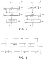
- first through N-th carrier signals c(1), c(2), ..., c(n), ... have different carrier frequencies as depicted with time t commonly scaled along abscissae and with an amplitude A scaled along each ordinate.
- a superposed carrier signal of the first through the N-th carrier signals has a waveform exemplified at the bottom.
- these carrier signals are digitally modulated into OFDM modulated signals, which are summed up into a composite OFDM modulated signal.
- OFDM modulated signals Four-phase quadrature phase shift keying (QPSK) is most frequently used for digital modulation.
- QPSK quadrature phase shift keying
- QAM quadrature amplitude modulation
- the composite modulated signal is transmitted as data symbols.
- Each data symbol lasts during a data symbol interval consisting of an effective symbol interval Eff sym and a guard interval GI.
- Such effective symbol intervals are used in actually transmitting the parallel data of the type described in conjunction with Fig. 1.
- the guard interval is a redundant interval for reducing adverse effects caused by multipath. In such guard intervals, the waveform of the effective symbol intervals is cyclically used.
- a frequency difference between two adjacent carrier signals is equal to an inverse number of the effective symbol interval.
- a frequency spectrum of each digitally modulated signal has zero points coincident with the carrier frequencies of other modulated signals and is subjected to no interference with the carrier signals.
- the OFDM modulated signal has an approximately rectangular power spectrum illustrated with a frequency f scaled along the abscissa and with the amplitude A scaled along the ordinate.
- a plurality of the data symbols are grouped into each of successive frames of a common frame period F by adding a few frame synchronizing symbols Ssym to each frame.
- data symbols of a predetermined integer are included in each frame following the frame synchronizing symbols.
- each frame additionally includes at least one service identification symbol.
- a transmitter frequency converter (FREQ CON) 29 frequency converts the baseband analog signal into a transmission signal TX.
- the inverse discrete Fourier converter 27 produces the data sample values which are equal in number to 2 k in each effective symbol interval Eff sym as scaled along a bottom row by 0, 1, 2, ..., and 2 k , where k represents a positive integer.
- Each data symbol therefore consists of 2 k (1 + r(G)) sample values, where r(G) represents a ratio of the guard interval to the effective symbol interval.
- the receiver device 23 comprises a receiver frequency converter (FREQ CON) 31 for frequency converting the transmission signal propagated thereto to a baseband received signal.
- FREQ CON receiver frequency converter
- FDFC forward discrete Fourier transform circuit or converter
- the forward discrete converter 33 Forward discrete Fourier converting the reception sample sequence onto a frequency domain and calculating phases and amplitudes of frequency components of the respective carrier frequencies, the forward discrete converter 33 produces reproductions of the first through the N-th parallel data which are designated by using the reference symbols C(1), C(2), ..., and C(N).
- a parallel to serial converter (P/S) 35 converts the reproductions to the sequence of data used in the transmitter device. In this manner, the receiver device 23 produces a data sequence reproduction RX.
- a controllable clock generator (not herein shown) is used to produce the receiver sampling clock sequence with a controllable sampling frequency. Based on the receiver sampling clock sequence, a receiver baseband clock sequence is produced. Furthermore, receiver frame, symbol, and data clock sequences are used together with the receiver sampling clock sequence in the forward discrete Fourier converter 33 and are derived from the receiver sampling clock sequence.
- AFC Automatic frequency control
- the sampling, the frame, the symbol, and the data clock sequences must also be subjected to automatic frequency control to insure correct operation of the forward discrete Fourier converter 33.
- the samples must be sampled from the received signal exactly 2 k (1 + r(G)) times per symbol.
- a transmitter device is for use in an OFDM digital communication system according to a first embodiment of the present invention.
- This transmitter device corresponds to the transmitter device 21 described in conjunction with Fig. 1 and comprises a serial to parallel converter, an inverse discrete Fourier converter, and a transmitter frequency converter which are labelled like in Fig. 1 and are designated by the reference numerals 25, 27, and 29.
- the transmitter device comprises a synchronizing symbol memory 41 which is preliminarily stored with a frame synchronizing symbol to produce a sequence or succession of synchronizing symbols.
- a symbol switch 43 is connected to the inverse discrete Fourier converter 27 and to the synchronizing symbol memory 41.
- a digital to analog converter (D/A) 45 is interposed between the symbol switch 43 and the frequency converter 29.
- a transmitter clock oscillator 47 generates a transmitter clock oscillation.
- a transmitter clock generator 49 Connected to the clock oscillator 47, a transmitter clock generator 49 produces a transmitter sampling clock sequence CLK, a transmitter frame clock sequence FCLK, a transmitter symbol clock sequence SCLK, and a transmitter data clock sequence DCLK.
- the sampling clock sequence is delivered to the digital to analog converter 45.
- the frame and the symbol clock sequences are delivered to the symbol switch 43.
- the serial to parallel converter 25 and the inverse discrete Fourier converter 27 are supplied from the clock generator 49 with various clock sequences.
- the data sequence DS is a sequence of binary bits such as "1" and/or "0" data.
- the serial to parallel converter 25 segments the sequence of data into blocks, each consisting of a preselected number of bits.
- the preselected number is typically decided between two and eight.
- the bits of the preselected number are represented by a complex number.
- the serial to parallel converter 25 supplies the inverse discrete Fourier converter 27 with such complex numbers, N in total, at a time as a parallel datum for modulating a certain one of the carrier signals described in connection with Fig. 2.
- the inverse discrete Fourier converter 27 converts such parallel data into the data sample values on the time axis. This inverse discrete Fourier conversion is carried out once in each symbol interval defined by the symbol clock sequence.
- Each data sample is a quantized digital datum of, for example, eight quantization bits at one of sampling instants indicated in Fig. 5 by short upright lines along the bottom row. Incidentally, the number of quantization bits should be decided in compliance with the manner of modulation, such as the four-phase quadrature phase shift keying.
- the frame clock sequence defines a frame period of successive frames for use in the transmission signal TX produced by the transmitter device.
- the symbol switch 43 picks up one of the synchronizing symbols from the sequence of synchronizing symbols and places this one of the synchronizing symbols in a first symbol interval in each frame period.
- the symbol switch 43 places data symbols from a sequence of data sample values produced by the inverse discrete Fourier converter 27.
- the symbol switch 43 consecutively picks up two synchronizing symbols to place these synchronizing symbols in the first and the second symbol intervals.
- the symbol switch 43 composes the data frames of the type illustrated with reference to Fig. 4. It is convenient to say that the symbol switch 43 adds synchronizing patterns to the frames and uses at least one of the synchronizing patterns as one of the synchronizing patterns in each frame.
- the transmitter sampling clock sequence has a transmitter sampling frequency.
- the transmitter frame clock sequence has a transmitter frame frequency which defines the frame period and is equal to a first inverse integral multiple of the sampling frequency.
- the transmitter symbol clock sequence has a transmitter symbol frequency which defines the symbol interval and is equal to a second integral multiple of the frame frequency.
- the clock generator 49 consequently frequency divides the clock oscillation into the sampling and other clock sequences.
- the clock generator 49 may include a local oscillator for generating, for example, the symbol clock sequence.
- the local oscillator must, however, be phase-locked to the clock oscillator 47.
- the symbol switch 43 produces a sequence of frames as the baseband transmission signal of the type which is described before. Each frame consists of digital sample values.
- the digital to analog converter 45 converts the baseband transmission signal to the analog baseband signal.
- the frequency converter 29 frequency converts the analog baseband signal to an RF or an IF transmission signal TX.
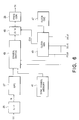
- a receiver device is a counterpart device of the transmitter device.
- the receiver device therefore corresponds to the receiver device 23 of Fig. 1 and comprises a receiver frequency converter, a forward discrete Fourier transform circuit or converter, and a parallel to serial converter which are designated by the reference numerals 31, 33, and 35.
- an analog to digital converter (A/D) 51 is separately illustrated between the frequency converter 31 and the discrete Fourier converter 33.
- a synchronization pattern memory 53 is preliminarily stored with a stored pattern to produce a stored pattern sequence or succession. The stored pattern is identical with the synchronizing symbol in the manner which will shortly be described.
- a cross-correlation calculator 55 is connected to the analog to serial converter 51 and to the synchronization memory 53. The cross-correlation calculator 55 calculates a cross-correlation value Xcor which will presently be described and is briefly called a correlation value. Accordingly, the cross-correlation calculator 55 will hereinafter be referred to in short as a correlation calculator 55.
- a maximum selector 57 is connected to the correlation calculator 55.
- An interval detector 59 is connected to the maximum selector 57.
- a frequency controller 61 is connected to the interval selector 59.
- a controllable oscillator, such as a voltage controlled oscillator (VCO), 63 is controlled by the frequency controller 61.
- a receiver clock generator 65 is connected to the controllable oscillator 63 and produces various receiver clock sequences, such as a receiver sampling clock sequence, a receiver frame clock sequence, a receiver symbol clock sequence, and a receiver data clock sequence which are designated by the reference symbols used for the transmitter clock generator 49 and have a receiver sampling frequency, a receiver frame frequency, a receiver symbol frequency, and a receiver data frequency.
- time t is indicated along each abscissa with an amplitude A indicated along each ordinate.
- a sweep signal has a frequency which is monotonously swept from a low frequency to a high frequency.
- a pseudonoise or PN signal has an amplitude which randomly varies between a high and a low level.
- the transmission signal TX is supplied to the frequency converter 31 and is converted to a baseband received signal.
- the analog to digital converter 51 samples the received signal and produces a reception sample sequence RS.
- Each reception sample has a sample value represented by, for example, eight bits at each sampling instant. Such sample values are successively produced as a sample value time sequence.
- the forward discrete Fourier converter 33 converts the sample values into complex data representative of complex values in the frequency domain in each symbol interval.
- the discrete Fourier converter 33 thereby produces N parallel sequences of complex data.
- the parallel to serial converter 35 estimates, as estimated data, the binary data which are converted by the inverse discrete Fourier converter 27 into the transmission signal carried on the OFDM modulation carrier signals.
- a sequence of the estimated data is the data sequence reproduction RX.
- the synchronization pattern memory 53 stores the stored pattern as a digital datum of eight-bit values at each sample point. It is presumed that the synchronizing symbol is known on preliminary storing the stored pattern. It is preferred that the synchronizing symbol and consequently the stored pattern produces a sharp autocorrelation peak with a precision of the order of one to ten clocks. Examples of such a symbol or pattern is either the sweep signal or the PN signal illustrated with reference to Figs. 8 and 9.
- the correlation calculator 55 is supplied from the analog to digital converter 51 with the reception sample sequence RS and from the synchronization pattern memory 53 with the stored pattern sequence. In the reception sample sequence, some and others of the reception samples would be the synchronizing symbol Ssym and the data and other symbols Dsym.
- the correlation calculator 55 calculates the cross-correlation value Xcor between the stored pattern and each of the reception samples. It is, however, not yet certain where each synchronizing symbol is included in the reception sample sequence.
- the correlation calculator 55 therefore calculates the correlation value with a window of a symbol length stepwise shifted along the reception sample sequence.
- the window may be shifted by one to several samples.
- the window is moved relative to the reception sample sequence as indicated at W(t(i)), W(t(i+1)), W(t(i+2)), ..., W(t(j)), ... .
- positions of the reception sample sequence are herein called candidate patterns.
- the correlation calculator 55 produces successive cross-correlation or correlation values.
- the maximum selector 57 compares the successive correlation values with a threshold level. As depicted with time t along the abscissa and with the correlation value Xcor along the ordinate, the correlation value has peaks above the threshold level indicated by a horizontal dotted line at time points t(i+1), t(j), ... . Successively detecting maxima of the correlation values, the maximum selector 57 selects ones of the candidate patterns that give two successive maxima.
- the interval detector 59 measures a time interval F' between such two maxima. It is duly possible to understand that the frame period is known at the receiver device. When the time interval of maxima is substantially coincident with the frame period, the above-mentioned ones of the candidate patterns are synchronization patterns which are reproductions of the synchronizing symbols. The synchronization patterns are used to make the frequency converter 61 control the controllable oscillator 63 and eventually the sampling, the frame, the symbol, the data, and the like frequencies of the clock generator 65.
- the interval detector 59 measures the time interval of maxima in terms of sampling clocks as a detected count of the sampling clocks.
- the frame period is known as a reference count of the sampling clocks.
- the interval detector 59 compares the measured count with the reference count. If the controllable oscillator 63 is the voltage controlled oscillator, the frequency controller 61 supplies the voltage controlled oscillator 63 with a D.C. voltage which raises and reduces the oscillation frequency when the measured count is less and greater than the reference count.
- the receiver clock generator 65 may separately include a phase-locked oscillator like the transmitter clock generator 49.
- a receiver device is for use in an OFDM digital communication system according to a second embodiment of this invention. Similar parts are designated by like reference numerals.
- a transmitter device is similar in structure to that described with reference to Figs. 1 through 6 and 8 and 9.
- the synchronizing symbol memory 41 is, however, preliminarily stored with the stored symbol in which the synchronizing symbol follows as a main synchronizing symbol Msync an auxiliary synchronizing symbol Async preceding the main synchronizing symbol.
- the synchronizing symbol memory 41 produces the stored symbol sequence which repeatedly indicates the auxiliary and the main synchronizing symbols as the sequence of synchronizing symbols.
- the symbol switch 43 places the auxiliary and the main synchronizing symbols in the first and the second symbol intervals in each frame and the data symbols in other symbol intervals of the frame. In other respects, the transmitter device is not different in operation.
- auxiliary and the main synchronizing symbols are indicated by Async and Msync.
- the main synchronizing symbol is used to finely or minutely indicate a particular time instant on the time axis as above in one to ten samples.
- the auxiliary synchronizing symbol is used to coarsely or roughly indicate the particular time instant in ten to several hundred samples and has a waveform which can sufficiently rapidly be detected as compared with that of the main synchronizing symbol.
- Such a signal may be a null signal of giving no signal during one symbol interval.
- the signal may be a single carrier signal in which a sinusoidal signal of a sole frequency lasts during one symbol interval.
- the signal may be a multi-carrier signal into which sinusoidal signals of several frequencies are summed up.
- the frequency converter 31 produces a substantially direct-current component while the auxiliary synchronizing symbol lasts in the baseband received signal.
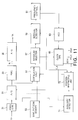
- the baseband received signal is supplied to an auxiliary synchronizing symbol detector which will be referred to briefly as an auxiliary detector 71.
- the auxiliary detector 71 produces an auxiliary position signal indicative of a position of the auxiliary synchronizing symbol in the received signal. It is possible to make the analog to digital converter 51 produce the auxiliary position signal indicative of the position not as an analog signal as described but as a digital signal. In this latter event, this digital auxiliary position signal is delivered to the auxiliary detector 71 in the manner depicted by a dashed line not from the frequency converter but from the analog to digital converter 51.
- a window position restricting unit 73 Responsive to the auxiliary position signal which may be either the analog or the digital signal, a window position restricting unit 73 roughly estimates position estimations where the main synchronizing symbol would successively appear in the received signal. On estimating the position estimations, the position restricting unit 73 uses the receiver sampling and symbol clock sequences and produces a gate signal which is switched to an on state during each interval in which each main synchronizing symbol appears in the received signal with a high probability.
- the stored pattern consists of the synchronization pattern which is now identical with the main synchronizing symbol.
- the correlation calculator 55 calculates the correlation values with the window stepwise shifted only while the gate signal is kept in the on state.
- the receiver device of Fig. 11 is operable like the receiver device illustrated with reference to Figs. 8 through 10.
- the position restricting unit 73 may turn the gate signal to the on state in response to the auxiliary position signal which is only once supplied thereto. In this event, the position restricting unit should thereafter switch the gate signal repeatedly to the on state at the frame period by counting clocks of either the sampling or the symbol clock sequence. It is now appreciated that a remarkable reduction is possible in an amount of calculation of the correlation values.
- a transmitter device is similar to that described with reference to Figs. 1 through 6 and 8 and 9.
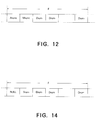
- the synchronizing symbol memory 41 is, however, preliminarily stored with the stored symbol in which the synchronizing symbol is preceded by a null symbol NULL representative of no signal during one symbol interval.
- the synchronizing symbol memory 41 produces the stored symbol sequence which repeatedly indicates the null and the synchronizing symbols as the sequence of synchronization patterns.
- FIG. 14 one frame of the successive frames is depicted as in Fig. 4 or 12.
- the null and the synchronizing symbols are indicated by NULL and Ssym.
- the null symbol is similar to the null signal described in connection with Fig. 12.
- the receiver device comprises a gate signal generator 75 connected to the clock generator 65.
- the gate signal generator 75 is connected to the frequency controller 61 through a gate signal line 77.
- the gate signal generator 75 Supplied with the receiver frame and symbol clock sequences from the clock generator 65, the gate signal generator 75 produces a gate signal turned to an on state in each frame period while the symbol clock sequence indicates a null period which the first symbol interval alone comprises.
- the gate signal is delivered to the frequency controller 61.
- the null period lasts one symbol interval at most.
- the controllable oscillator 63 is frequency controlled within a control interval which is shorter than one symbol interval.
- the frequency controller 61 controls the controllable oscillator 63 only while the gate signal is kept in the on state, namely, while the receiver frame and symbol clock sequences indicate the first symbol interval or shorter in each frame period. During a different period in each frame, the frequency controller 61 suspends control of the controllable oscillator 63. It is now understood that the controllable oscillator 63 is not controlled while the synchronizing symbol and the data symbols are sampled by the analog to digital converter 51 from the received signal and that the receiver clock generator 65 stably generates meanwhile the receiver clock sequence.
- a receiver device for use in an OFDM digital communication system according to a fourth embodiment of this invention. Similar parts are designated by like reference numerals.
- a transmitter device is not different from that described in conjunction with the receiver device illustrated with reference to Fig. 13.
- the synchronizing symbol sequence is as depicted in Fig. 12.
- the receiver device comprises the auxiliary device 71, the position restricting unit 73, the gate signal generator 75, and the gate signal line 77.
- the gate signal generator 75 gives the on state to the gate signal during the first symbol interval in each frame at the longest.
- the correlation calculator 55 and the frequency controller 61 are operable in the manner described in connection with Figs. 11 and 13, respectively. This receiver is therefore excellently operable as described in conjunction with Fig. 11 and additionally as described in connection with Fig. 13.
- a receiver device for use in an OFDM digital communication system according to a fifth embodiment of this invention. Similar parts are designated by like reference numerals. Using as a counterpart device the receiver device being illustrated, a transmitter device is not different from that described with reference to Figs. 1 through 6 and 8 and 9.
- the receiver device additionally comprises an interval averaging unit 79 between the interval detector 59 and the frequency controller 61.
- the interval averaging unit 79 may be referred to alternatively as an interval integrator 79.
- the interval detector 59 detects the time interval F' in terms of clocks of the received sampling clock signal and produces a clock count representative of the time interval each time whenever the synchronization pattern is detected. Responsive to the clock count, the interval averaging unit 79 calculates a mean interval of, or integrates, the time intervals represented by a prescribed number of the clock counts, such as from several clock counts to a few scores of clock counts. The preselected number is empirically decided in consideration of a rate of variation in either a noise level or in characteristics of a propagation path through which the transmission signal reaches the receiver device from the transmitter device. It is now appreciated that a stable control is possible on receiver clock frequencies by the mean value.
Landscapes
- Engineering & Computer Science (AREA)
- Computer Networks & Wireless Communication (AREA)
- Signal Processing (AREA)
- Synchronisation In Digital Transmission Systems (AREA)
- Stabilization Of Oscillater, Synchronisation, Frequency Synthesizers (AREA)
Applications Claiming Priority (2)
| Application Number | Priority Date | Filing Date | Title |
|---|---|---|---|
| JP6138386A JP2731722B2 (ja) | 1994-05-26 | 1994-05-26 | クロック周波数自動制御方式及びそれに用いる送信装置と受信装置 |
| JP138386/94 | 1994-05-26 |
Publications (2)
| Publication Number | Publication Date |
|---|---|
| EP0689313A2 true EP0689313A2 (fr) | 1995-12-27 |
| EP0689313A3 EP0689313A3 (fr) | 1999-02-10 |
Family
ID=15220735
Family Applications (1)
| Application Number | Title | Priority Date | Filing Date |
|---|---|---|---|
| EP95108089A Withdrawn EP0689313A3 (fr) | 1994-05-26 | 1995-05-26 | Commande automatique de fréquence pour signaux MDFO utilisant des fonctions de fenêtrage |
Country Status (4)
| Country | Link |
|---|---|
| US (1) | US5596582A (fr) |
| EP (1) | EP0689313A3 (fr) |
| JP (1) | JP2731722B2 (fr) |
| AU (1) | AU684154B2 (fr) |
Cited By (26)
| Publication number | Priority date | Publication date | Assignee | Title |
|---|---|---|---|---|
| WO1997048197A3 (fr) * | 1996-05-20 | 1997-12-18 | Adc Telecommunications Inc | Systeme de communication a transport telephonique par ondes porteuses multiples |
| WO1997027550A3 (fr) * | 1996-01-24 | 1998-03-05 | Adc Telecommunications Inc | Systeme de communication avec transmission telephonique par porteuses multiples |
| WO1998010547A3 (fr) * | 1996-09-02 | 1998-05-07 | Telia Ab | Perfectionnements relatifs a des systemes de transmission a porteuses multiples |
| WO1998010549A3 (fr) * | 1996-09-02 | 1998-05-22 | Telia Ab | Perfectionnements relatifs a des systemes de transmission a porteuses multiples |
| WO1998010546A3 (fr) * | 1996-09-02 | 1998-06-04 | Telia Ab | Perfectionnements relatifs a des systemes de transmission a porteuses multiples |
| WO1998026512A3 (fr) * | 1996-12-12 | 1998-07-30 | Nokia Telecommunications Oy | Procede de reception et recepteur |
| EP0822691A3 (fr) * | 1996-07-31 | 1999-08-25 | Victor Company Of Japan, Limited | Synchronisation de symbole dans un récepteur de signaux multiporteurs |
| WO1999044326A3 (fr) * | 1998-02-26 | 1999-11-11 | Wavesat Telecom Inc | Systeme de reception a multiplexage orthogonal par repartition en frequence |
| EP1047236A1 (fr) * | 1999-04-22 | 2000-10-25 | Abb Research Ltd. | Ynchronisation dans un système de transmission de données avec transformation rapide de Fourier |
| GB2352368A (en) * | 1999-07-19 | 2001-01-24 | Oak Technology Inc | Receiver circuit |
| EP1122650A3 (fr) * | 1996-01-24 | 2002-01-16 | ADC Telecommunications, Inc. | Système de communication de transmission téléphonique à porteuses multiples |
| EP0901260A3 (fr) * | 1997-05-12 | 2002-03-20 | Sony Corporation | Synchronisation de trames et de symbôles dans des récepteurs multiporteurs |
| EP1089510A3 (fr) * | 1999-09-30 | 2004-02-11 | Hitachi Denshi Kabushiki Kaisha | Procédé et dispositif de transmission de données utilisant un système OFDM |
| EP1492264A1 (fr) * | 2003-06-24 | 2004-12-29 | Lg Electronics Inc. | Dispositif et procédé de commande automatique de fréquence dans un terminal de communication mobile |
| WO2005004427A1 (fr) * | 2003-07-08 | 2005-01-13 | Thales | Methode d'estimation de residu de la porteuse, estimateur et systeme de modulation avec asservissement de la porteuse l'utilisant |
| EP1073241A3 (fr) * | 1999-07-29 | 2006-05-03 | Matsushita Electric Industrial Co., Ltd. | Synchronisation de symbôles pour la transmission multiporteuse |
| EP1675297A1 (fr) | 1999-02-24 | 2006-06-28 | Sony Deutschland Gmbh | Dispositif de réception et méthode de synchronisation dans un système de télécommunication numérique |
| GB2422278A (en) * | 2002-12-03 | 2006-07-19 | Synad Technologies Ltd | OFDM synchronisation using the correlation of an identification marker and a circular-shifted signal |
| EP1054540A3 (fr) * | 1999-04-30 | 2006-11-02 | Sony Corporation | Méthode, dispositif et récepteur pour la détection de la position du symbole nul |
| US7227834B1 (en) | 1999-08-27 | 2007-06-05 | Mitsubishi Kabushiki Kaisha | Synchronizing pulse generating method and method of receiving OFDM signal |
| WO2008110886A3 (fr) * | 2007-03-15 | 2009-09-24 | Nokia Corporation | Corrélation de recherche de service d'émission numérique |
| US7787548B2 (en) | 2007-03-15 | 2010-08-31 | Nokia Corporation | Digital broadcast service discovery correlation |
| US7796706B2 (en) | 2007-03-15 | 2010-09-14 | Nokia Corporation | Digital broadcast service discovery correlation |
| EP2017993A4 (fr) * | 2006-04-26 | 2011-12-28 | Panasonic Corp | Dispositif et procede de detection de signal |
| EP2267960A3 (fr) * | 2001-10-17 | 2012-08-01 | Nortel Networks Limited | Sélection de cellules dans des systèmes MIMO-OFDM |
| US8861622B2 (en) | 1999-02-24 | 2014-10-14 | Sony Deutschland Gmbh | Transmitting apparatus and method for a digital telecommunication system |
Families Citing this family (79)
| Publication number | Priority date | Publication date | Assignee | Title |
|---|---|---|---|---|
| JP2701745B2 (ja) * | 1994-07-27 | 1998-01-21 | 日本電気株式会社 | シンボルクロック制御装置 |
| US5774450A (en) * | 1995-01-10 | 1998-06-30 | Matsushita Electric Industrial Co., Ltd. | Method of transmitting orthogonal frequency division multiplexing signal and receiver thereof |
| USRE42236E1 (en) | 1995-02-06 | 2011-03-22 | Adc Telecommunications, Inc. | Multiuse subcarriers in multipoint-to-point communication using orthogonal frequency division multiplexing |
| US7280564B1 (en) | 1995-02-06 | 2007-10-09 | Adc Telecommunications, Inc. | Synchronization techniques in multipoint-to-point communication using orthgonal frequency division multiplexing |
| US5828696A (en) * | 1995-03-30 | 1998-10-27 | Lucent Technologies Inc. | Timing recovery in a network-synchronized modem |
| JP2802255B2 (ja) * | 1995-09-06 | 1998-09-24 | 株式会社次世代デジタルテレビジョン放送システム研究所 | 直交周波数分割多重伝送方式及びそれを用いる送信装置と受信装置 |
| DE19538302C2 (de) * | 1995-10-16 | 2001-03-22 | Bosch Gmbh Robert | Verfahren zur terrestrischen Übertragung digitaler Signale |
| DE69711957T2 (de) | 1996-02-02 | 2002-09-19 | Deutsche Thomson-Brandt Gmbh | Verfahren und Einrichtung zum Empfang von Mehrträgersignalen |
| CA2183140C (fr) * | 1996-08-12 | 2001-11-20 | Telecommunications Research Laboratories | Systeme de synchronisation et de restitution de frequence |
| US5995483A (en) | 1996-08-22 | 1999-11-30 | Tellabs Operations, Inc. | Apparatus and method for upstream clock synchronization in a multi-point OFDM/DMT digital communication system |
| US5790514A (en) * | 1996-08-22 | 1998-08-04 | Tellabs Operations, Inc. | Multi-point OFDM/DMT digital communications system including remote service unit with improved receiver architecture |
| US6122246A (en) * | 1996-08-22 | 2000-09-19 | Tellabs Operations, Inc. | Apparatus and method for clock synchronization in a multi-point OFDM/DMT digital communications system |
| US6771590B1 (en) | 1996-08-22 | 2004-08-03 | Tellabs Operations, Inc. | Communication system clock synchronization techniques |
| US6285654B1 (en) * | 1996-08-22 | 2001-09-04 | Tellabs Operations, Inc. | Apparatus and method for symbol alignment in a multi-point OFDM or DMT digital communications system |
| US6118758A (en) * | 1996-08-22 | 2000-09-12 | Tellabs Operations, Inc. | Multi-point OFDM/DMT digital communications system including remote service unit with improved transmitter architecture |
| US6950388B2 (en) * | 1996-08-22 | 2005-09-27 | Tellabs Operations, Inc. | Apparatus and method for symbol alignment in a multi-point OFDM/DMT digital communications system |
| US6108319A (en) * | 1996-11-05 | 2000-08-22 | Worldspace International Networks, Inc. | Satellite payload processing system providing on-board rate alignment |
| JPH10190612A (ja) * | 1996-12-26 | 1998-07-21 | Sony Corp | 通信方法及び受信装置 |
| KR100239475B1 (ko) * | 1996-12-31 | 2000-01-15 | 구자홍 | 에이치디 티브이의 동기신호 검출장치 |
| JP3568180B2 (ja) | 1997-06-12 | 2004-09-22 | 株式会社日立国際電気 | データ伝送装置 |
| US6151296A (en) * | 1997-06-19 | 2000-11-21 | Qualcomm Incorporated | Bit interleaving for orthogonal frequency division multiplexing in the transmission of digital signals |
| EP0895387A1 (fr) * | 1997-07-28 | 1999-02-03 | Deutsche Thomson-Brandt Gmbh | Détection du mode de transmission d'un signal vidéo numérique télédiffusé |
| US5991289A (en) * | 1997-08-05 | 1999-11-23 | Industrial Technology Research Institute | Synchronization method and apparatus for guard interval-based OFDM signals |
| DE19743169A1 (de) * | 1997-09-30 | 1999-04-01 | Daimler Benz Ag | Verfahren zur Rahmensynchronisation eines Empfangssignals |
| US6731711B1 (en) * | 1997-11-19 | 2004-05-04 | Lg Electronics Inc. | Signal recovery system |
| JP3568182B2 (ja) * | 1997-12-03 | 2004-09-22 | 株式会社日立国際電気 | データ伝送装置の同期検出方法及びその装置 |
| US6226336B1 (en) * | 1998-02-20 | 2001-05-01 | Telefonaktiebolaget Lm Ericsson (Publ) | Method and apparatus for detecting a frequency synchronization signal |
| US6631175B2 (en) * | 1998-04-03 | 2003-10-07 | Tellabs Operations, Inc. | Spectrally constrained impulse shortening filter for a discrete multi-tone receiver |
| US7440498B2 (en) * | 2002-12-17 | 2008-10-21 | Tellabs Operations, Inc. | Time domain equalization for discrete multi-tone systems |
| DK1068704T3 (da) | 1998-04-03 | 2012-09-17 | Tellabs Operations Inc | Filter til impulssvarforkortning, med yderligere spektrale begrænsninger, til multibærebølgeoverførsel |
| US6144413A (en) * | 1998-06-25 | 2000-11-07 | Analog Devices, Inc. | Synchronization signal detection and phase estimation apparatus and method |
| US6356608B1 (en) * | 1998-06-29 | 2002-03-12 | Telefonaktiebolaget Lm Ericsson (Publ) | Method, apparatus, and system for determining a location of a frequency synchronization signal |
| US6111919A (en) * | 1999-01-20 | 2000-08-29 | Intellon Corporation | Synchronization of OFDM signals |
| US6539063B1 (en) | 1999-02-18 | 2003-03-25 | Ibiquity Digital Corporation | System and method for recovering symbol timing offset and carrier frequency error in an OFDM digital audio broadcast system |
| JP3252820B2 (ja) * | 1999-02-24 | 2002-02-04 | 日本電気株式会社 | 復調及び変調回路並びに復調及び変調方法 |
| JP2000269919A (ja) * | 1999-03-16 | 2000-09-29 | Matsushita Electric Ind Co Ltd | Ofdm通信装置 |
| US6748481B1 (en) * | 1999-04-06 | 2004-06-08 | Microsoft Corporation | Streaming information appliance with circular buffer for receiving and selectively reading blocks of streaming information |
| US6269132B1 (en) | 1999-04-26 | 2001-07-31 | Intellon Corporation | Windowing function for maintaining orthogonality of channels in the reception of OFDM symbols |
| US6074086A (en) * | 1999-04-26 | 2000-06-13 | Intellon Corporation | Synchronization of OFDM signals with improved windowing |
| US6891792B1 (en) * | 1999-05-14 | 2005-05-10 | At&T Corp. | Method for estimating time and frequency offset in an OFDM system |
| US6940933B1 (en) | 1999-06-23 | 2005-09-06 | Cingular Wireless Ii, Llc | Apparatus and method for synchronization in a multiple-carrier communications system by observing a phase-frequency relationship of a plurality of pilot signals |
| US6768714B1 (en) | 1999-06-23 | 2004-07-27 | At&T Wireless Services, Inc. | Methods and apparatus for use in obtaining frequency synchronization in an OFDM communication system |
| US6930995B1 (en) | 1999-06-23 | 2005-08-16 | Cingular Wireless Ii, Llc | Apparatus and method for synchronization in a multiple-carrier communication system by observing a plurality of synchronization indicators |
| US6700866B1 (en) | 1999-06-23 | 2004-03-02 | At&T Wireless Services, Inc. | Methods and apparatus for use in obtaining frequency synchronization in an OFDM communication system |
| US6389087B1 (en) | 1999-06-23 | 2002-05-14 | At&T Wireless Services, Inc. | Apparatus and method for synchronization in a multiple-carrier communication system by observing energy within a guard band |
| US6445423B1 (en) * | 1999-07-09 | 2002-09-03 | Thomson Licensing S.A. | Controlled oscillator in a digital symbol timing recovery network |
| US6661771B1 (en) * | 1999-09-17 | 2003-12-09 | Lucent Technologies Inc. | Method and apparatus for interleaver synchronization in an orthogonal frequency division multiplexing (OFDM) communication system |
| US6836518B1 (en) | 1999-11-16 | 2004-12-28 | Hitachi Kokusai Electric Inc. | Synchronization control method for receiver apparatus of data transmission system utilizing orthogonal frequency division multiplex, and data transmission system |
| JP4329192B2 (ja) * | 1999-11-19 | 2009-09-09 | ソニー株式会社 | 無線通信装置、無線通信システムおよびその方法 |
| KR100345329B1 (ko) * | 1999-12-24 | 2002-07-24 | 삼성탈레스 주식회사 | 직교 주파수 분할 다중화 수신기에서의 샘플링 클럭 복원 장치 및 그 방법 |
| US6704374B1 (en) * | 2000-02-16 | 2004-03-09 | Thomson Licensing S.A. | Local oscillator frequency correction in an orthogonal frequency division multiplexing system |
| US7106821B2 (en) * | 2000-03-15 | 2006-09-12 | Sony Corporation | Data modulation method, data modulation device and communication device |
| US6529868B1 (en) * | 2000-03-28 | 2003-03-04 | Tellabs Operations, Inc. | Communication system noise cancellation power signal calculation techniques |
| US6560303B1 (en) * | 2000-10-26 | 2003-05-06 | Comsat Corporation | Joint frame, carrier and clock synchronization scheme |
| JP2002290367A (ja) * | 2001-03-26 | 2002-10-04 | Hitachi Kokusai Electric Inc | 帯域分割復調方法及びofdm受信機 |
| JP3850695B2 (ja) * | 2001-08-07 | 2006-11-29 | シャープ株式会社 | 受信装置 |
| US7142502B2 (en) * | 2001-08-30 | 2006-11-28 | Intel Corporation | Technique for continuous OFDM demodulation |
| JP3835800B2 (ja) * | 2002-02-08 | 2006-10-18 | 株式会社東芝 | 受信フレームの同期方法、および、受信装置 |
| WO2004036821A1 (fr) * | 2002-10-18 | 2004-04-29 | Koninklijke Philips Electronics N.V. | Appareil de traitement de donnees identifiant une frequence d'horloge de communication |
| EP1652207A4 (fr) * | 2003-06-05 | 2011-12-28 | Meshnetworks Inc | Systeme et procede de determination d'un point de synchronisation dans des modems ofdm pour une mesure exacte du temps de vol |
| DE10334064B3 (de) * | 2003-07-25 | 2005-04-14 | Infineon Technologies Ag | Verfahren und Schaltungsanordnung zum Kalibrieren eines den Abtastzeitpunkt eines Empfangssignals beeinflussenden Abtastungssteuersignales eines Abtastphasenauswahlelements |
| JP4097615B2 (ja) * | 2004-03-23 | 2008-06-11 | 三洋電機株式会社 | 信号検出方法および装置ならびにそれを利用した送信装置および受信装置 |
| JP4313715B2 (ja) * | 2004-04-01 | 2009-08-12 | Okiセミコンダクタ株式会社 | 同期確立回路および同期確立方法 |
| TWI297570B (en) * | 2005-02-17 | 2008-06-01 | Ind Tech Res Inst | Symbol timing synchronization system for orthogonal frequency division multiplexing system |
| US7606498B1 (en) * | 2005-10-21 | 2009-10-20 | Nortel Networks Limited | Carrier recovery in a coherent optical receiver |
| JP4527101B2 (ja) * | 2006-11-20 | 2010-08-18 | 日本電信電話株式会社 | バースト無線信号伝送システム、無線送信装置、無線受信装置及びバースト無線信号伝送方法 |
| US8526524B2 (en) * | 2007-03-27 | 2013-09-03 | Qualcomm Incorporation | Orthogonal reference signal permutation |
| US8159241B1 (en) * | 2007-04-24 | 2012-04-17 | Marvell International Ltd. | Method and apparatus for on-chip adjustment of chip characteristics |
| US7652980B2 (en) | 2007-11-02 | 2010-01-26 | Nokia Corporation | Orthogonal frequency division multiplexing synchronization |
| KR20110026479A (ko) * | 2008-07-07 | 2011-03-15 | 스미토모덴키고교가부시키가이샤 | 기지국 장치 |
| US8363635B2 (en) * | 2008-08-20 | 2013-01-29 | Wei Chi Liu | Method and system for reducing power consumption of signal synchronization |
| US8665691B2 (en) * | 2009-02-05 | 2014-03-04 | Sony Corporation | Frame and data pattern structure for multi-carrier systems |
| WO2014024407A1 (fr) * | 2012-08-08 | 2014-02-13 | ルネサスエレクトロニクス株式会社 | Dispositif de détection |
| JP5962987B2 (ja) * | 2012-09-28 | 2016-08-03 | パナソニックIpマネジメント株式会社 | 同期システムとそれを備えた受信装置、同装置を備えた通信システム、及び同期方法 |
| JP5962988B2 (ja) * | 2012-09-28 | 2016-08-03 | パナソニックIpマネジメント株式会社 | 通信システム、それに用いられる送信器と受信器、及び通信方法 |
| JP5942226B2 (ja) * | 2012-11-13 | 2016-06-29 | パナソニックIpマネジメント株式会社 | 通信システム、それに用いられる送信器と受信器、及び通信方法 |
| CN107204944B (zh) * | 2016-03-18 | 2020-11-03 | 富士通株式会社 | 发送序列产生装置、训练序列同步装置、信道间隔估计装置、方法和系统 |
| WO2018035719A1 (fr) * | 2016-08-23 | 2018-03-01 | 华为技术有限公司 | Procédé d'acquisition de signal de discrimination de phase dans un circuit de récupération d'horloge, et discriminateur de phase |
| JP2018042220A (ja) * | 2016-09-09 | 2018-03-15 | 富士通株式会社 | クロック再生回路,半導体集積回路装置およびrfタグ |
Citations (2)
| Publication number | Priority date | Publication date | Assignee | Title |
|---|---|---|---|---|
| WO1992005646A1 (fr) | 1990-09-14 | 1992-04-02 | National Transcommunications Limited | Reception de signaux multiplexes de division de frequence orthogonale (ofdm) |
| WO1992010043A1 (fr) | 1990-11-30 | 1992-06-11 | Thomson-Csf | Procede de recalage des oscillateurs locaux d'un recepteur et dispositif pour la mise en ×uvre du procede |
Family Cites Families (8)
| Publication number | Priority date | Publication date | Assignee | Title |
|---|---|---|---|---|
| US4291409A (en) * | 1978-06-20 | 1981-09-22 | The Mitre Corporation | Spread spectrum communications method and apparatus |
| US4414676A (en) * | 1981-03-31 | 1983-11-08 | Motorola, Inc. | Signal synchronization system |
| DE3333714A1 (de) * | 1983-09-17 | 1985-04-04 | Standard Elektrik Lorenz Ag, 7000 Stuttgart | Schaltungsanordnung zur rahmen- und phasensynchronisation eines empfangsseitigen abtasttaktes |
| US4829543A (en) * | 1987-12-04 | 1989-05-09 | Motorola, Inc. | Phase-coherent TDMA quadrature receiver for multipath fading channels |
| DE4128713A1 (de) * | 1991-08-29 | 1993-03-04 | Daimler Benz Ag | Verfahren und anordnung zur messung der traegerfrequenzablage in einem mehrkanaluebertragungssystem |
| JP2904986B2 (ja) * | 1992-01-31 | 1999-06-14 | 日本放送協会 | 直交周波数分割多重ディジタル信号送信装置および受信装置 |
| JPH0746217A (ja) * | 1993-07-26 | 1995-02-14 | Sony Corp | ディジタル復調装置 |
| US5444697A (en) * | 1993-08-11 | 1995-08-22 | The University Of British Columbia | Method and apparatus for frame synchronization in mobile OFDM data communication |
-
1994
- 1994-05-26 JP JP6138386A patent/JP2731722B2/ja not_active Expired - Lifetime
-
1995
- 1995-05-25 US US08/450,540 patent/US5596582A/en not_active Expired - Lifetime
- 1995-05-26 AU AU20341/95A patent/AU684154B2/en not_active Expired
- 1995-05-26 EP EP95108089A patent/EP0689313A3/fr not_active Withdrawn
Patent Citations (4)
| Publication number | Priority date | Publication date | Assignee | Title |
|---|---|---|---|---|
| WO1992005646A1 (fr) | 1990-09-14 | 1992-04-02 | National Transcommunications Limited | Reception de signaux multiplexes de division de frequence orthogonale (ofdm) |
| JPH06501357A (ja) | 1990-09-14 | 1994-02-10 | ナショナル・トランスコミュニケーションズ・リミテッド | 直交周波数分割多重化信号の受信 |
| WO1992010043A1 (fr) | 1990-11-30 | 1992-06-11 | Thomson-Csf | Procede de recalage des oscillateurs locaux d'un recepteur et dispositif pour la mise en ×uvre du procede |
| JPH05504037A (ja) | 1990-11-30 | 1993-06-24 | トムソン―セーエスエフ | 受信器の局部発振器を整合する方法及びその方法を実施するための装置 |
Cited By (51)
| Publication number | Priority date | Publication date | Assignee | Title |
|---|---|---|---|---|
| US8638655B2 (en) | 1994-09-26 | 2014-01-28 | Htc Corporation | Systems and method for orthogonal frequency divisional multiplexing |
| US8547824B2 (en) | 1994-09-26 | 2013-10-01 | Htc Corporation | Systems and methods for orthogonal frequency divisional multiplexing |
| US6292651B1 (en) | 1995-02-06 | 2001-09-18 | Adc Telecommunications, Inc. | Communication system with multicarrier transport distribution network between a head end terminal and remote units |
| US8576693B2 (en) | 1995-02-06 | 2013-11-05 | Htc Corporation | Systems and method for orthogonal frequency division multiplexing |
| US7957265B2 (en) * | 1995-02-06 | 2011-06-07 | Adc Telecommunications, Inc. | Systems and method for orthogonal frequency divisional multiplexing |
| WO1997027550A3 (fr) * | 1996-01-24 | 1998-03-05 | Adc Telecommunications Inc | Systeme de communication avec transmission telephonique par porteuses multiples |
| EP1122650A3 (fr) * | 1996-01-24 | 2002-01-16 | ADC Telecommunications, Inc. | Système de communication de transmission téléphonique à porteuses multiples |
| WO1997048197A3 (fr) * | 1996-05-20 | 1997-12-18 | Adc Telecommunications Inc | Systeme de communication a transport telephonique par ondes porteuses multiples |
| EP0822691A3 (fr) * | 1996-07-31 | 1999-08-25 | Victor Company Of Japan, Limited | Synchronisation de symbole dans un récepteur de signaux multiporteurs |
| US6091702A (en) * | 1996-07-31 | 2000-07-18 | Victor Company Of Japan, Ltd. | Method and apparatus for symbol synchronization in orthogonal frequency division multiplexing systems |
| WO1998010546A3 (fr) * | 1996-09-02 | 1998-06-04 | Telia Ab | Perfectionnements relatifs a des systemes de transmission a porteuses multiples |
| US6181714B1 (en) | 1996-09-02 | 2001-01-30 | Telia Ab | Multi-carrier transmission systems |
| WO1998010549A3 (fr) * | 1996-09-02 | 1998-05-22 | Telia Ab | Perfectionnements relatifs a des systemes de transmission a porteuses multiples |
| WO1998010547A3 (fr) * | 1996-09-02 | 1998-05-07 | Telia Ab | Perfectionnements relatifs a des systemes de transmission a porteuses multiples |
| US6359926B1 (en) * | 1996-09-02 | 2002-03-19 | Stmicroelectronics N.V. | Multi-carrier transmission systems |
| US6363128B1 (en) * | 1996-09-02 | 2002-03-26 | Stmicroelectronics N.V. | Multi-carrier transmission systems |
| WO1998026512A3 (fr) * | 1996-12-12 | 1998-07-30 | Nokia Telecommunications Oy | Procede de reception et recepteur |
| US6690756B1 (en) | 1996-12-12 | 2004-02-10 | Nokia Corporation | Synchronization method and receiver comprising multiplication means, transform and comparison means |
| EP0901260A3 (fr) * | 1997-05-12 | 2002-03-20 | Sony Corporation | Synchronisation de trames et de symbôles dans des récepteurs multiporteurs |
| WO1999044326A3 (fr) * | 1998-02-26 | 1999-11-11 | Wavesat Telecom Inc | Systeme de reception a multiplexage orthogonal par repartition en frequence |
| US6151295A (en) * | 1998-02-26 | 2000-11-21 | Wavesat Telecom Inc. | OFDM receiving system |
| US9438289B2 (en) | 1999-02-24 | 2016-09-06 | Sony Deutschland Gmbh | Transmitting apparatus and method for receiving a digital signal in a digital telecommunication system |
| US8861622B2 (en) | 1999-02-24 | 2014-10-14 | Sony Deutschland Gmbh | Transmitting apparatus and method for a digital telecommunication system |
| US9450627B2 (en) | 1999-02-24 | 2016-09-20 | Sony Deutschland Gmbh | Transmitting apparatus and method for receiving a digital signal in a digital telecommunication system |
| EP1675297A1 (fr) | 1999-02-24 | 2006-06-28 | Sony Deutschland Gmbh | Dispositif de réception et méthode de synchronisation dans un système de télécommunication numérique |
| EP1717984A1 (fr) | 1999-02-24 | 2006-11-02 | Sony Deutschland Gmbh | Dispositif de réception et méthode de synchronisation dans un système de télécommunication numérique |
| EP1047236A1 (fr) * | 1999-04-22 | 2000-10-25 | Abb Research Ltd. | Ynchronisation dans un système de transmission de données avec transformation rapide de Fourier |
| EP1054540A3 (fr) * | 1999-04-30 | 2006-11-02 | Sony Corporation | Méthode, dispositif et récepteur pour la détection de la position du symbole nul |
| GB2352368A (en) * | 1999-07-19 | 2001-01-24 | Oak Technology Inc | Receiver circuit |
| US7349497B1 (en) | 1999-07-19 | 2008-03-25 | Conexant Systems, Inc. | Receiver circuit |
| EP1073241A3 (fr) * | 1999-07-29 | 2006-05-03 | Matsushita Electric Industrial Co., Ltd. | Synchronisation de symbôles pour la transmission multiporteuse |
| US7227834B1 (en) | 1999-08-27 | 2007-06-05 | Mitsubishi Kabushiki Kaisha | Synchronizing pulse generating method and method of receiving OFDM signal |
| US7020116B1 (en) | 1999-09-30 | 2006-03-28 | Hitachi Denshi Kabushiki Kaisha | Method and apparatus of data transmission |
| EP1089510A3 (fr) * | 1999-09-30 | 2004-02-11 | Hitachi Denshi Kabushiki Kaisha | Procédé et dispositif de transmission de données utilisant un système OFDM |
| US8830816B2 (en) | 2001-10-17 | 2014-09-09 | Apple Inc. | System access and synchronization methods for MIMO OFDM communications systems and physical layer packet and preamble design |
| US8441918B2 (en) | 2001-10-17 | 2013-05-14 | Apple Inc. | System access and synchronization methods for MIMO OFDM communications systems and physical layer packet and preamble design |
| EP2267960A3 (fr) * | 2001-10-17 | 2012-08-01 | Nortel Networks Limited | Sélection de cellules dans des systèmes MIMO-OFDM |
| GB2422278B (en) * | 2002-12-03 | 2007-04-04 | Synad Technologies Ltd | Method and device for synchronisation in OFDM |
| US7596154B2 (en) | 2002-12-03 | 2009-09-29 | Synad Technologies Limited | Method and device for synchronisation in OFDM |
| GB2422278A (en) * | 2002-12-03 | 2006-07-19 | Synad Technologies Ltd | OFDM synchronisation using the correlation of an identification marker and a circular-shifted signal |
| EP1492264A1 (fr) * | 2003-06-24 | 2004-12-29 | Lg Electronics Inc. | Dispositif et procédé de commande automatique de fréquence dans un terminal de communication mobile |
| US7308238B2 (en) | 2003-06-24 | 2007-12-11 | Lg Electronics Inc. | Automatic frequency controlling apparatus and method of mobile communication terminal |
| WO2005004427A1 (fr) * | 2003-07-08 | 2005-01-13 | Thales | Methode d'estimation de residu de la porteuse, estimateur et systeme de modulation avec asservissement de la porteuse l'utilisant |
| US7129802B2 (en) | 2003-07-08 | 2006-10-31 | Thales | Method for estimating a carrier leak, an estimator and modulation system provided with automatic control of a carrier using said system |
| FR2857532A1 (fr) * | 2003-07-08 | 2005-01-14 | Thales Sa | Methode d'estimation de residu de la porteuse, estimateur et systeme de modulation avec asservissement de la porteuse l'utilisant |
| EP2017993A4 (fr) * | 2006-04-26 | 2011-12-28 | Panasonic Corp | Dispositif et procede de detection de signal |
| US7787548B2 (en) | 2007-03-15 | 2010-08-31 | Nokia Corporation | Digital broadcast service discovery correlation |
| RU2441335C2 (ru) * | 2007-03-15 | 2012-01-27 | Нокиа Корпорейшн | Корреляция для обнаружения услуг цифрового вещания |
| US8054910B2 (en) | 2007-03-15 | 2011-11-08 | Nokia Corporation | Digital broadcast service discovery correlation |
| US7796706B2 (en) | 2007-03-15 | 2010-09-14 | Nokia Corporation | Digital broadcast service discovery correlation |
| WO2008110886A3 (fr) * | 2007-03-15 | 2009-09-24 | Nokia Corporation | Corrélation de recherche de service d'émission numérique |
Also Published As
| Publication number | Publication date |
|---|---|
| AU684154B2 (en) | 1997-12-04 |
| JPH07321762A (ja) | 1995-12-08 |
| AU2034195A (en) | 1995-12-07 |
| EP0689313A3 (fr) | 1999-02-10 |
| US5596582A (en) | 1997-01-21 |
| JP2731722B2 (ja) | 1998-03-25 |
Similar Documents
| Publication | Publication Date | Title |
|---|---|---|
| US5596582A (en) | AFC in OFDM modulation by shift of a window along a reception sample sequence | |
| EP0712555B1 (fr) | Procede et appareil de synchronisation dans des systemes de transmission numerique a multiplexage par repartition orthogonale de la frequence | |
| US6035003A (en) | Apparatus for correcting frequency offset in OFDM receiving system | |
| EP0829988B1 (fr) | Synchronisation par symbole et réglage de la fréquence d'échantillonnage dans un récepteur pour MDFO | |
| US7336598B2 (en) | Guard interval length control method in OFDM system and OFDM transmitting and receiving apparatuses | |
| US6058101A (en) | Synchronization method and system for a digital receiver | |
| US6590872B1 (en) | Receiver with parallel correlator for acquisition of spread spectrum digital transmission | |
| EP1041790B1 (fr) | Synchronisation de symbole pour démodulateur OFDM | |
| JP4043335B2 (ja) | 受信装置 | |
| US6993084B1 (en) | Coarse frequency synchronisation in multicarrier systems | |
| US6621857B1 (en) | Carrier tracking loop for direct sequence spread spectrum systems | |
| JP3242287B2 (ja) | 無線通信システムおよび通信装置 | |
| US5903614A (en) | Communication method and receiving apparatus | |
| US6381251B1 (en) | Data transmission apparatus and receiving apparatus using orthogonal frequency division multiplex modulation system | |
| EP0605188A2 (fr) | Synchronisation de symbole et de trame pour un système TDMA | |
| US6252908B1 (en) | Method and device in a communication system | |
| JPH08256094A (ja) | 時分割多元接続システムおよび符号分割多元接続システムの両方における記号およびフレームの同期 | |
| WO1996002990A2 (fr) | Procede et dispositif de synchronisation d'un emetteur et d'un recepteur dans un systeme numerique | |
| EP1089510A2 (fr) | Procédé et dispositif de transmission de données utilisant un système OFDM | |
| KR19980703715A (ko) | 다중캐리어 변조 시스템의 결합 주파수 오프셋과 타이밍 추정을 위한 방법 및 그 장치 | |
| CN101743729A (zh) | 使用滤波器组的多载波接收器的健壮同步的方法和对应的接收器与收发器 | |
| JPH1065605A (ja) | 受信方法、タイミング検出装置及び受信装置 | |
| JP3116377B2 (ja) | クロック回復回路で用いられる位相調整方法および装置 | |
| US5255292A (en) | Method and apparatus for modifying a decision-directed clock recovery system | |
| US6836518B1 (en) | Synchronization control method for receiver apparatus of data transmission system utilizing orthogonal frequency division multiplex, and data transmission system |
Legal Events
| Date | Code | Title | Description |
|---|---|---|---|
| PUAI | Public reference made under article 153(3) epc to a published international application that has entered the european phase |
Free format text: ORIGINAL CODE: 0009012 |
|
| AK | Designated contracting states |
Kind code of ref document: A2 Designated state(s): DE FR GB |
|
| PUAL | Search report despatched |
Free format text: ORIGINAL CODE: 0009013 |
|
| AK | Designated contracting states |
Kind code of ref document: A3 Designated state(s): DE FR GB |
|
| 17P | Request for examination filed |
Effective date: 19990318 |
|
| 17Q | First examination report despatched |
Effective date: 20011026 |
|
| STAA | Information on the status of an ep patent application or granted ep patent |
Free format text: STATUS: THE APPLICATION IS DEEMED TO BE WITHDRAWN |
|
| 18D | Application deemed to be withdrawn |
Effective date: 20030828 |