EP0689340A2 - Signalverarbeitungsschaltkreis - Google Patents
Signalverarbeitungsschaltkreis Download PDFInfo
- Publication number
- EP0689340A2 EP0689340A2 EP95108224A EP95108224A EP0689340A2 EP 0689340 A2 EP0689340 A2 EP 0689340A2 EP 95108224 A EP95108224 A EP 95108224A EP 95108224 A EP95108224 A EP 95108224A EP 0689340 A2 EP0689340 A2 EP 0689340A2
- Authority
- EP
- European Patent Office
- Prior art keywords
- converter
- voltage
- limit reference
- data
- analog
- Prior art date
- Legal status (The legal status is an assumption and is not a legal conclusion. Google has not performed a legal analysis and makes no representation as to the accuracy of the status listed.)
- Granted
Links
- 238000006243 chemical reaction Methods 0.000 description 77
- 230000003321 amplification Effects 0.000 description 13
- 238000003199 nucleic acid amplification method Methods 0.000 description 13
- 238000010276 construction Methods 0.000 description 6
- 238000010586 diagram Methods 0.000 description 4
- 238000000034 method Methods 0.000 description 2
- 230000008569 process Effects 0.000 description 2
- 230000008859 change Effects 0.000 description 1
- 230000010354 integration Effects 0.000 description 1
- 238000012986 modification Methods 0.000 description 1
- 230000004048 modification Effects 0.000 description 1
- 238000009966 trimming Methods 0.000 description 1
Images


Classifications
-
- H—ELECTRICITY
- H04—ELECTRIC COMMUNICATION TECHNIQUE
- H04N—PICTORIAL COMMUNICATION, e.g. TELEVISION
- H04N1/00—Scanning, transmission or reproduction of documents or the like, e.g. facsimile transmission; Details thereof
- H04N1/40—Picture signal circuits
- H04N1/407—Control or modification of tonal gradation or of extreme levels, e.g. background level
- H04N1/4076—Control or modification of tonal gradation or of extreme levels, e.g. background level dependent on references outside the picture
Definitions
- the present invention relates to an image-inputting apparatus, and more specifically concerns a signal-processing circuit that converts analog voltages obtained by reading a document by using a line sensor into digital data and releases the data.
- an image-inputting apparatus which is used in facsimiles, digital copying machines, scanners and other apparatuses, is provided with a line sensor 51 for reading an original document 50.
- the line sensor 51 has a construction wherein light-receiving elements are aligned in a straight-line shape.
- the analog signals from the line sensor 51 are converted into digital signals by a signal-processing circuit.
- Fig. 5 shows one example of the signal-processing circuit wherein CCDs (Charge Coupled Devices) are used as the light-receiving elements of the line sensor 51.
- CCDs Charge Coupled Devices
- the signal-processing circuit is provided with an amplification section 52 for amplifying such a minute output from the line sensor 51 to an appropriate level and an A/D (analog/digital) converter 53 for converting a signal from the amplification section 52 into a digital signal.
- an amplification section 52 for amplifying such a minute output from the line sensor 51 to an appropriate level
- an A/D (analog/digital) converter 53 for converting a signal from the amplification section 52 into a digital signal.
- a lower-limit reference voltage (Vref-), which is used in the A/D converter 53, is obtained by converting data from a black-correction-value storing section 54 into analog signals by using a D/A (digital/analog) converter 55, and an upper-limit reference voltage (Vref+), which is also used in the A/D converter 53, is obtained by converting data from a white-correction-value storing section 56 into analog signals by using a D/A (digital/analog) converter 57.
- the black-correction-value storing section 54 stores output voltage values (output voltages in the dark state) from the CCDs as its data that are obtained when no light illuminates the line sensor 51
- the white-correction-value storing section 56 stores output voltage values (output voltages in the bright state) from the CCDs as its data that are obtained when light reflected from a white plate illuminates the line sensor 51.
- Fig. 6 shows a basic construction of a flash-type A/D converter which is capable of providing high-speed conversion that is suitable for the line sensor 51 consisting of CCDs.
- the resolution of the A/D converter 53 is improved, the input capacity increases because of an increased degree of integration; this makes it difficult to operate the A/D converter 53 at high frequencies. Furthermore, it is necessary to provide a trimming process in order to increase accuracy of resistances of the resistors 61 that divide the potential difference between the reference values Vref+ and Vref-. For this reason, it is actually very difficult to realize a resolution of more than 10 bits.
- Japanese Laid-Open Patent Application No.108867/1991 discloses an image-reading apparatus wherein signals, accumulated in the image sensor, are read out a plurality of times in a divided manner.
- a plurality of divided areas are provided between the white-correction value and the black-correction value; the upper limit and the lower limit of each area are defined as Vref+ and Vref- respectively; and an analog-to-digital conversion is carried out for each area.
- the signal-processing circuit of the present invention is provided with: the first and second A/D converters for converting analog voltages from a line sensor into digital data; the first reference-voltage setting means for setting a lower-limit reference voltage and an upper-limit reference voltage for the first A/D converter; a data-storing section for storing digital data obtained by the first A/D converter; and the second reference-voltage setting means for setting a lower-limit reference voltage for the second A/D converter to a voltage that is lower than the voltage corresponding to the digital data stored in the data-storing section and that is higher than the lower-limit reference voltage set by the first reference-voltage setting means, as well as for setting a upper-limit reference voltage for the second A/D converter to a voltage that is higher than the voltage corresponding to the digital data stored in the data-storing section and that is lower than the upper-limit reference voltage set by the first reference-voltage setting means.
- the signal-processing circuit is characterized in that the digital data is released
- the first reference-voltage setting means sets the lower-limit reference voltage and the upper-limit reference voltage for the first A/D converter. Under these settings, the first A/D converter is allowed to convert analog voltages from the line sensor into digital data.
- the data-storing section stores the digital data.
- the second reference-voltage setting means sets the lower-limit reference voltage for the second A/D converter to a voltage that is lower than the voltage corresponding to the digital data stored in the data-storing section and that is higher than the lower-limit reference voltage set by the first reference-voltage setting means, and also sets the upper-limit reference voltage for the second A/D converter to a voltage that is higher than the voltage corresponding to the digital data stored in the data-storing section and that is lower than the upper-limit reference voltage set by the first reference-voltage setting means. Therefore, the voltage range from the lower-limit reference voltage to the upper-limit reference voltage in the second A/D converter is smaller than the corresponding voltage range in the first A/D converter.
- the second A/D converter converts analog voltages from the line sensor into digital data. For this reason, even if A/D converters having the same resolution are used as the first and second A/D converters, it is possible to provide a higher resolution in the second A/D converter than in the first A/D converter. This makes it possible to realize a signal-processing circuit with high resolution at low costs. Moreover, it is possible to achieve a high-speed processing since the reading operation is carried out with high resolution only in the vicinity of the voltage corresponding to the digital data.
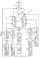
- Fig. 1 which shows one embodiment of the present invention, is a block diagram showing a schematic construction of a signal-processing circuit.
- Fig. 2 is an explanatory drawing that shows an operation of the signal-processing circuit of Fig. 1.
- Fig. 3 which shows another embodiment of the present invention, is a block diagram showing a schematic construction of a signal-processing circuit.
- Fig. 4 is an explanatory drawing that shows a conventional image-inputting apparatus.
- Fig. 5 is a block diagram showing a schematic construction of a signal-processing circuit for use in the image-inputting apparatus of Fig. 4.
- Fig. 6 which shows one example of an A/D converter in the signal-processing circuit of Fig. 5, is a block diagram showing a schematic construction of a flash-type A/D converter.
- the signal-processing circuit of the present embodiment is provided with: an amplification section 2 for amplifying a minute output from a line sensor 1, an A/D conversion system 3 for converting a signal from the amplification section 2 into a digital signal, an A/D conversion system 4 for converting the signal from the amplification section 2 into a digital signal with a resolution higher than that in the A/D conversion system 3, and a multiplexer 5 that allows the A/D conversion system 4 to release the digital signal when there is no error in the A/D conversion system 4 and that allows the A/D conversion system 3 to release the digital signal in the event of an error in the A/D conversion system 4.
- the A/D conversion system 3 is provided with: a black-correction value storing section 11, a D/A converter 12 for digital-to-analog converting data from the black-correction value storing section 11, an analog subtraction circuit 13 for subtracting an output signal from the D/A converter 12 from an output signal of the amplification section 2, and an A/D converter 14 (the first A/D converter) for analog-to-digital converting a signal from the analog subtraction circuit 13.
- the result of the analog-to-digital conversion, obtained from the A/D converter 14, is written to a data-storing section 21, which will be described later, and the result of the analog-to-digital conversion corresponding to one-line portion, stored in the data-storing section 21, is utilized in an analog-to-digital conversion for the next line.
- the A/D conversion system 3 is further provided with: a white-correction value storing section 15, a digital subtraction circuit 16 for subtracting data from the black-correction value storing section 11 from data from the white-correction value storing section 15, and a D/A converter 17 for digital-to-analog converting an output signal from the digital subtraction circuit 16.
- the lower-limit reference voltage (Vref-) of the A/D converter 14 is set to 0V (ground level), and the upper-limit reference voltage (Vref+) is set to the output voltage from the D/A converter 17.
- the black-correction value storing section 11 the white-correction value storing section 15, the digital subtraction circuit 16 and the D/A converter 17 constitute the first reference-voltage setting means.
- the A/D conversion system 4 is provided with: a data-storing section 21 for storing the result of an analog-to- digital conversion obtained from a line immediately before the line currently being read by the line sensor 1, a subtraction circuit 22 for subtracting a value X (which will be described later) from data from the data-storing section 21, a D/A converter 23 for digital-to-analog converting an output from the subtraction circuit 22, an A/D converter 24 (second A/D converter) for analog-to-digital converting an output signal from the analog subtraction circuit 13 in the A/D conversion system 3, and a digital addition circuit 25 for adding the output signal from the A/D converter 24 and the output signal from the subtraction circuit 22.
- the A/D converter 24 releases an error signal in the event of an error, and the error signal is inputted to a select terminal of the multiplexer 5.
- the A/D conversion system 4 is further provided with an addition circuit 26 for adding the value X to data from the data-storing section 21 and a D/A converter 27 for digital-to-analog converting an output signal from the addition circuit 26.
- the lower-limit reference voltage (Vref-) of the A/D converter 24 is set to the output voltage of the D/A converter 23, and the upper-limit reference voltage (Vref+) is set to the output voltage of the D/A converter 27.
- the subtraction circuit 22, the D/A converter 23, the addition circuit 26, and the D/A converter 27 constitute the second reference-voltage setting means.
- an output signal from the D/A converter 17 in the A/D conversion system 3 is inputted to the reference inputs (ref) of the D/A converters 23 and 27.
- the signal from the line sensor 1 is amplified by the amplification section 2, and the resulting output signal from the amplification section 2 is inputted to the analog subtraction circuit 13.
- the analog subtraction circuit 13 the output signal from the D/A converter 12 is subtracted from the output signal from the amplification section 2. Then, the output signal from the analog subtraction circuit 13 is inputted to the A/D converter 14 in the A/D conversion system 3 as well as to the A/D converter 24 in the A/D conversion system 4, where the analog-to-digital conversion is carried out.
- the signal to be inputted to the A/D converters 14 and 24 is represented by s - b.
- b is an analog value corresponding to B.
- digital data is represented by a capital English letter, and the corresponding analog value is represented by the corresponding small English letter.
- the output of the A/D converter 24 is represented by S - B - (S - B)' + X , and the resolution is 2x/2 n in the case of the A/D converter 24 with n bits.
- the output of the A/D conversion system 4 that is, the output of the digital addition circuit 25, is represented by S - B, and the resolution is 2x/2 n .
- the value X when there is a correlation between a line currently being read by the line sensor 1 and the preceding line, it is possible to set the value X to a value that satisfies (S - B)' - X ⁇ S - B ⁇ (S - B)' + X and that is substantially smaller than S - B.
- the resolution of the A/D conversion system 4, 2x/2 n becomes substantially smaller than the resolution of the A/D conversion system 3, (w - b)/2 n .
- A/D converters 14 and 24 having the same resolution of n bits are used, it is possible to obtain a result of analog-to-digital conversion with higher resolution in the A/D conversion system 4 than in the A/D conversion system 3.
- the multiplexer 5 selects the result of analog-to-digital conversion in the A/D conversion system 3, and outputs the selected result.
- the result of analog-to-digital conversion with normal resolution, that is, with the resolution of (w - b)/2 n , even when there is hardly any correlation between the two lines.
- the A/D converter 24 when it has an overflow or an underflow, sends an error signal to the multiplexer 5 not for each line, but for each pixel on the line; therefore, the multiplexer 5 selects either the result of analog-to-digital conversion of the A/D conversion system 3, or the result of analog-to-digital conversion of the A/D conversion system 4 for each pixel, and outputs the selected result.
- This arrangement makes it possible to obtain a result of analog-to-digital conversion with high resolution for almost all pixels in the case of normal images that seldom have abrupt changes in contrast.
- the output of the D/A converter 17 in the A/D conversion system 3, that is, w - b, is inputted to the reference inputs (ref) of the D/A converters 23 and 27; this allows the D/A converters 23 and 27 to always execute digital-to-analog conversions over all the range of W - B.
- the result of analog-to-digital conversion in the line immediately before a line currently being read is stored in the data-storing section 21; however, this is not necessarily limited to the line immediately before a line currently being read, and a result of analog-to-digital conversion in any pixel may be stored in the data-storing section 21, as long as it is a pixel portion located in the vicinity of a pixel currently being read.
- r represents the resolution of the A/D converter 14, that is, (w - b)/28 . Therefore, X is determined so as to satisfy the following equation.
- the data to be stored in the data-storing section 21 are only regarded as reference values to set the input range of the A/D converter 24.
- 8 bits provide a sufficient accuracy.
- 2 bits are added to low order position, and these are set to 0. The same is also true in the case of the output of the A/D converter 14.
- the signal-processing circuit of the present embodiment is different from that of the aforementioned embodiment in that an A/D converter 31 (the first and second A/D converters), which is commonly used in the A/D conversion system 3 as well as in the A/D conversion system 4, is installed instead of the A/D converters 14 and 24, and in that a switching circuit 32 for switching voltages to be applied to the Vref+ and Vref- of the A/D converter 31 is installed.
- this change makes the multiplexer 5 unnecessary.
- the signal from the line sensor 1 is amplified by the amplification section 2, and the output signal from the amplification section 2 is inputted to the analog subtraction circuit 13.
- the analog subtraction circuit 13 the output signal from the D/A converter 12 is subtracted from the output signal from the amplification section 2. Then, the output signal from the analog subtraction circuit 13 is inputted to the A/D converter 31, where an analog-to-digital conversion having a normal resolution is conducted on one line by the A/D conversion system 3 and then an analog-to-digital conversion having a high resolution is conducted on the same line by the A/D conversion system 4.
- the switching circuit 32 is switched to the A/D conversion system 3 side by a control means (not shown).
- the Vref+ and Vref- of the A/D converter 31 are respectively set to the output voltage (that is, w - b) from the D/A converter 17 and 0 V (that is, ground level), in the same manner as in the aforementioned embodiment.
- the output of the A/D conversion system 3 that is, the output of the A/D converter 31, is represented by S - B in the same manner as in the aforementioned embodiment, and its resolution is (w - b)/2 n in the case of the A/D converter 31 with n bits.
- the switching circuit 32 is switched to the A/D conversion system 4 side by the control means.
- the Vref+ and Vref- of the A/D converter 31 are respectively set to the output voltage (that is, (s - b)' + x ) from the D/A converter 27 and the output voltage (that is, (s - b)' - x ) from the D/A converter 23, in the same manner as in the aforementioned embodiment.
- the prime symbol (') represents the result of analog-to-digital conversion conducted by the A/D conversion system 3.
- the output of the A/D converter 31 is represented by S - B - (S - B)' + X , in the same manner as in the aforementioned embodiment, and its resolution is 2x/2 n in the case of the A/D converter 31 with n bits.
- the output of the A/D conversion system 4 that is, the output of the digital addition circuit 25 is represented by S - B, and its resolution is 2x/2 n .
- the A/D conversion systems 3 and 4 conduct analog-to-digital conversions on the same line, it is possible to set the value X to a value that always satisfies (S - B)' - X ⁇ S - B ⁇ (S - B)' + X and that is smaller than S - B. Therefore, the resolution of the A/D conversion system 4, 2x/2 n , is substantially smaller than the resolution of the A/D conversion system 3, (w - b)/2 n . In other words, even if the A/D converters 14 and 24 having the same resolution of n bits are used, the A/D conversion system 4 provides a result of analog-to-digital conversion having a higher resolution than the A/D conversion system 3.
- the A/D converter 31 is commonly used in the A/D conversion system 3 as well as in the A/D conversion system 4; this makes it possible to reduce the cost of the signal-processing circuit more than the aforementioned embodiment.
Landscapes
- Engineering & Computer Science (AREA)
- Multimedia (AREA)
- Signal Processing (AREA)
- Analogue/Digital Conversion (AREA)
- Image Input (AREA)
- Facsimile Image Signal Circuits (AREA)
Applications Claiming Priority (3)
| Application Number | Priority Date | Filing Date | Title |
|---|---|---|---|
| JP14010394 | 1994-06-22 | ||
| JP06140103A JP3091084B2 (ja) | 1994-06-22 | 1994-06-22 | 信号処理回路 |
| JP140103/94 | 1994-06-22 |
Publications (3)
| Publication Number | Publication Date |
|---|---|
| EP0689340A2 true EP0689340A2 (de) | 1995-12-27 |
| EP0689340A3 EP0689340A3 (de) | 1996-12-11 |
| EP0689340B1 EP0689340B1 (de) | 2000-08-09 |
Family
ID=15261017
Family Applications (1)
| Application Number | Title | Priority Date | Filing Date |
|---|---|---|---|
| EP95108224A Expired - Lifetime EP0689340B1 (de) | 1994-06-22 | 1995-05-29 | Signalverarbeitungsschaltkreis |
Country Status (4)
| Country | Link |
|---|---|
| US (1) | US5606321A (de) |
| EP (1) | EP0689340B1 (de) |
| JP (1) | JP3091084B2 (de) |
| DE (1) | DE69518283T2 (de) |
Cited By (2)
| Publication number | Priority date | Publication date | Assignee | Title |
|---|---|---|---|---|
| EP0920193A3 (de) * | 1997-11-29 | 2000-06-07 | Samsung Electronics Co., Ltd. | Bildverarbeitungsvorrichtung und -verfahren |
| WO2014029411A1 (de) * | 2012-08-21 | 2014-02-27 | Technische Hochschule Mittelhessen | Analog -digital wandler |
Families Citing this family (3)
| Publication number | Priority date | Publication date | Assignee | Title |
|---|---|---|---|---|
| US6275259B1 (en) | 1998-02-02 | 2001-08-14 | International Business Machines Corporation | Digital automatic gain control circuit for image system |
| US6720899B2 (en) * | 2001-08-07 | 2004-04-13 | Hrl Laboratories, Llc | Extended precision pixel |
| JP4581820B2 (ja) * | 2005-04-28 | 2010-11-17 | 王子製紙株式会社 | 配向測定装置および配向測定方法 |
Citations (1)
| Publication number | Priority date | Publication date | Assignee | Title |
|---|---|---|---|---|
| JPH03108867A (ja) | 1989-04-28 | 1991-05-09 | Canon Inc | 画像読取装置 |
Family Cites Families (14)
| Publication number | Priority date | Publication date | Assignee | Title |
|---|---|---|---|---|
| JPS54964A (en) * | 1977-06-06 | 1979-01-06 | Fujitsu Ltd | Analog digital converter |
| JPS55145431A (en) * | 1979-04-28 | 1980-11-13 | Jeol Ltd | A/d converter |
| JPS57160221A (en) * | 1981-03-28 | 1982-10-02 | Olympus Optical Co Ltd | Analog to digital conversion system |
| JPS58104524A (ja) * | 1981-12-17 | 1983-06-22 | Sony Corp | A/dコンバ−タ回路 |
| JPS58158566A (ja) * | 1982-03-17 | 1983-09-20 | Hitachi Ltd | 検査装置 |
| JPS5959035U (ja) * | 1982-10-09 | 1984-04-17 | ソニー株式会社 | A−d変換装置 |
| JPS59119921A (ja) * | 1982-12-25 | 1984-07-11 | Toshiba Corp | アナログ・デイジタル変換器 |
| JPS6365719A (ja) * | 1986-09-05 | 1988-03-24 | Nec Corp | 映像信号処理装置 |
| US4947168A (en) * | 1988-05-23 | 1990-08-07 | Hughes Aircraft Company | Subranging analog-to-digital converter with calibration |
| US5267053A (en) * | 1988-10-27 | 1993-11-30 | Eastman Kodak Company | Automatic reference control for image scanners |
| JPH02311083A (ja) * | 1989-05-26 | 1990-12-26 | Ricoh Co Ltd | 原稿読取装置 |
| US5053771A (en) * | 1990-07-16 | 1991-10-01 | Eastman Kodak Company | Adaptive dual range analog to digital converter |
| US5262873A (en) * | 1990-11-07 | 1993-11-16 | Canon Kabushiki Kaisha | Image signal correcting in image data processing requiring only small memory capacity |
| US5231398A (en) * | 1992-04-24 | 1993-07-27 | Panasonic Technologies, Inc. | Method and apparatus for self-tracking multiple analog to digital conversion |
-
1994
- 1994-06-22 JP JP06140103A patent/JP3091084B2/ja not_active Expired - Lifetime
-
1995
- 1995-05-12 US US08/440,483 patent/US5606321A/en not_active Expired - Lifetime
- 1995-05-29 DE DE69518283T patent/DE69518283T2/de not_active Expired - Fee Related
- 1995-05-29 EP EP95108224A patent/EP0689340B1/de not_active Expired - Lifetime
Patent Citations (1)
| Publication number | Priority date | Publication date | Assignee | Title |
|---|---|---|---|---|
| JPH03108867A (ja) | 1989-04-28 | 1991-05-09 | Canon Inc | 画像読取装置 |
Cited By (2)
| Publication number | Priority date | Publication date | Assignee | Title |
|---|---|---|---|---|
| EP0920193A3 (de) * | 1997-11-29 | 2000-06-07 | Samsung Electronics Co., Ltd. | Bildverarbeitungsvorrichtung und -verfahren |
| WO2014029411A1 (de) * | 2012-08-21 | 2014-02-27 | Technische Hochschule Mittelhessen | Analog -digital wandler |
Also Published As
| Publication number | Publication date |
|---|---|
| EP0689340A3 (de) | 1996-12-11 |
| JPH088745A (ja) | 1996-01-12 |
| JP3091084B2 (ja) | 2000-09-25 |
| US5606321A (en) | 1997-02-25 |
| DE69518283D1 (de) | 2000-09-14 |
| EP0689340B1 (de) | 2000-08-09 |
| DE69518283T2 (de) | 2001-01-04 |
Similar Documents
| Publication | Publication Date | Title |
|---|---|---|
| US5278658A (en) | Image reading apparatus having a function for correcting dark signals generated in a photoelectric conversion element | |
| US7349134B2 (en) | Image reading apparatus | |
| US20140043514A1 (en) | Solid-state image pickup device and signal processing method therefor | |
| EP0150329B1 (de) | Darstellungs- und Korrektursystem für Bildsignale | |
| US5606321A (en) | Signal-processing circuit | |
| US4768015A (en) | A/D converter for video signal | |
| US5191445A (en) | Image reader | |
| JPH03503703A (ja) | Ccd素子からの暗電流及びオフセット電圧を補償する方法及び装置 | |
| EP0767577B1 (de) | Bildverarbeitungsvorrichtung mit Bildvergrösserungsfunktion | |
| EP1049323A2 (de) | Bildlesegerät | |
| US7751097B2 (en) | Methods and apparatuses for changing driving sequence to output charge coupled device signal | |
| GB2154827A (en) | Method for correcting picture signals in image input equipment | |
| JP2618655B2 (ja) | 画像読み取り装置 | |
| JPS59123367A (ja) | 画像読取り方式 | |
| US6700682B1 (en) | Image processing system capable of easily changing subscanning magnification in image read | |
| JPH0425283A (ja) | 画像読み取り装置 | |
| KR102011945B1 (ko) | 열 병렬 아날로그 디지털 변환기의 블랙 레벨 보상 장치 | |
| KR100267246B1 (ko) | 광전변환센서의구동제어장치 | |
| JPH0310463A (ja) | 画像読取装置 | |
| KR100271155B1 (ko) | 광전 변환 센서의 구동 신호 발생 회로 | |
| JPS6129275A (ja) | 中間調画像の補正方法 | |
| JPS62296655A (ja) | 連続階調画の表示システム | |
| JP2889079B2 (ja) | スキャナ | |
| JPH04371073A (ja) | 画像読取装置 | |
| JPH04196760A (ja) | 画像読み取り処理装置 |
Legal Events
| Date | Code | Title | Description |
|---|---|---|---|
| PUAI | Public reference made under article 153(3) epc to a published international application that has entered the european phase |
Free format text: ORIGINAL CODE: 0009012 |
|
| AK | Designated contracting states |
Kind code of ref document: A2 Designated state(s): DE FR GB |
|
| PUAL | Search report despatched |
Free format text: ORIGINAL CODE: 0009013 |
|
| AK | Designated contracting states |
Kind code of ref document: A3 Designated state(s): DE FR GB |
|
| 17P | Request for examination filed |
Effective date: 19970304 |
|
| 17Q | First examination report despatched |
Effective date: 19980925 |
|
| GRAG | Despatch of communication of intention to grant |
Free format text: ORIGINAL CODE: EPIDOS AGRA |
|
| GRAG | Despatch of communication of intention to grant |
Free format text: ORIGINAL CODE: EPIDOS AGRA |
|
| GRAH | Despatch of communication of intention to grant a patent |
Free format text: ORIGINAL CODE: EPIDOS IGRA |
|
| GRAH | Despatch of communication of intention to grant a patent |
Free format text: ORIGINAL CODE: EPIDOS IGRA |
|
| GRAA | (expected) grant |
Free format text: ORIGINAL CODE: 0009210 |
|
| AK | Designated contracting states |
Kind code of ref document: B1 Designated state(s): DE FR GB |
|
| REF | Corresponds to: |
Ref document number: 69518283 Country of ref document: DE Date of ref document: 20000914 |
|
| ET | Fr: translation filed | ||
| PLBE | No opposition filed within time limit |
Free format text: ORIGINAL CODE: 0009261 |
|
| STAA | Information on the status of an ep patent application or granted ep patent |
Free format text: STATUS: NO OPPOSITION FILED WITHIN TIME LIMIT |
|
| 26N | No opposition filed | ||
| REG | Reference to a national code |
Ref country code: GB Ref legal event code: IF02 |
|
| PGFP | Annual fee paid to national office [announced via postgrant information from national office to epo] |
Ref country code: FR Payment date: 20090515 Year of fee payment: 15 Ref country code: DE Payment date: 20090527 Year of fee payment: 15 |
|
| PGFP | Annual fee paid to national office [announced via postgrant information from national office to epo] |
Ref country code: GB Payment date: 20090527 Year of fee payment: 15 |
|
| GBPC | Gb: european patent ceased through non-payment of renewal fee |
Effective date: 20100529 |
|
| REG | Reference to a national code |
Ref country code: FR Ref legal event code: ST Effective date: 20110131 |
|
| PG25 | Lapsed in a contracting state [announced via postgrant information from national office to epo] |
Ref country code: DE Free format text: LAPSE BECAUSE OF NON-PAYMENT OF DUE FEES Effective date: 20101201 |
|
| PG25 | Lapsed in a contracting state [announced via postgrant information from national office to epo] |
Ref country code: FR Free format text: LAPSE BECAUSE OF NON-PAYMENT OF DUE FEES Effective date: 20100531 |
|
| PG25 | Lapsed in a contracting state [announced via postgrant information from national office to epo] |
Ref country code: GB Free format text: LAPSE BECAUSE OF NON-PAYMENT OF DUE FEES Effective date: 20100529 |