EP0689366B1 - Circuit de détection de tonalité téléphonique - Google Patents
Circuit de détection de tonalité téléphonique Download PDFInfo
- Publication number
- EP0689366B1 EP0689366B1 EP95410049A EP95410049A EP0689366B1 EP 0689366 B1 EP0689366 B1 EP 0689366B1 EP 95410049 A EP95410049 A EP 95410049A EP 95410049 A EP95410049 A EP 95410049A EP 0689366 B1 EP0689366 B1 EP 0689366B1
- Authority
- EP
- European Patent Office
- Prior art keywords
- processing units
- memory
- signal
- values
- addresses
- Prior art date
- Legal status (The legal status is an assumption and is not a legal conclusion. Google has not performed a legal analysis and makes no representation as to the accuracy of the status listed.)
- Expired - Lifetime
Links
- 238000001514 detection method Methods 0.000 title claims description 11
- 230000015654 memory Effects 0.000 claims description 81
- 238000005070 sampling Methods 0.000 claims description 19
- 230000010354 integration Effects 0.000 claims description 3
- 102100032919 Chromobox protein homolog 1 Human genes 0.000 description 9
- 101000797584 Homo sapiens Chromobox protein homolog 1 Proteins 0.000 description 9
- 230000006399 behavior Effects 0.000 description 3
- 230000005540 biological transmission Effects 0.000 description 3
- 238000001914 filtration Methods 0.000 description 3
- 230000001934 delay Effects 0.000 description 1
- 230000003111 delayed effect Effects 0.000 description 1
- 238000011084 recovery Methods 0.000 description 1
- 239000007858 starting material Substances 0.000 description 1
Images

Classifications
-
- H—ELECTRICITY
- H04—ELECTRIC COMMUNICATION TECHNIQUE
- H04Q—SELECTING
- H04Q1/00—Details of selecting apparatus or arrangements
- H04Q1/18—Electrical details
- H04Q1/30—Signalling arrangements; Manipulation of signalling currents
- H04Q1/44—Signalling arrangements; Manipulation of signalling currents using alternate current
- H04Q1/444—Signalling arrangements; Manipulation of signalling currents using alternate current with voice-band signalling frequencies
- H04Q1/45—Signalling arrangements; Manipulation of signalling currents using alternate current with voice-band signalling frequencies using multi-frequency signalling
- H04Q1/457—Signalling arrangements; Manipulation of signalling currents using alternate current with voice-band signalling frequencies using multi-frequency signalling with conversion of multifrequency signals into digital signals
-
- H—ELECTRICITY
- H04—ELECTRIC COMMUNICATION TECHNIQUE
- H04Q—SELECTING
- H04Q1/00—Details of selecting apparatus or arrangements
- H04Q1/18—Electrical details
- H04Q1/30—Signalling arrangements; Manipulation of signalling currents
- H04Q1/44—Signalling arrangements; Manipulation of signalling currents using alternate current
Definitions
- the present invention relates to a modular structure programmable to detect various telephone tones which vary from one standard of telephone transmission to another and from one country to another.
- the present invention more generally relates to the detection of identification signals in a digital signal to using a set of processing modules which can be programmatically interconnected by a user.
- a identification signal is generally characterized by a amplitude exceeding, at a predetermined frequency, a threshold or the amplitude of another identification signal.
- the processing modules include filters programmable, rectification and integration modules (power estimators), and comparators.
- Rockwell company markets detection circuit tone including three times serial association a programmable filter, a power estimator, and a comparator.
- This tone detector has only two configurations programmable. In a first configuration, each of the three filters receives the digital signal to be processed, which can detect three different tones. In the second configuration, the three filters are connected in series in order to ability to detect a tone in a narrow frequency band.
- This structure which is known from document GB-A-2 255 472, is far from being able to adapt to all possible tone detection situations.
- An object of the present invention is to provide a programmable signal processing structure that can adapt to virtually any situation in the field in which programmable structure is used.
- Another object of the present invention is to achieve a structure particularly simple and easy to program.
- the present invention provides a circuit for detecting identification signals in an input digital signal which has values arriving at a sampling frequency, comprising a set of modules freely programmable interconnected processing units by a user; an updated signal memory at the sampling frequency of the input signal, containing the values of the output signals from the processing modules and the input signal to associated addresses; a programming memory containing, in locations associated with entries processing modules, addresses of the signal memory associated with the signals that the user wishes to connect to said starters; and control means for reading the addresses stored in the programming memory, read the values finding at these addresses in the signal memory, and providing these values read at the inputs of the processing modules in a order corresponding to the locations of the programming memory.
- the circuit includes an input memory in which the values read are stored in associated locations respectively at the inputs of the processing modules.
- the processing modules include first modules of processing and second processing modules to which are associated respectively a first programming memory and a second programming memory, the control means being intended to read the addresses stored in the first and second programming memories at different frequencies, read the values found at these addresses in the signal memory, and supply these values read to the inputs of the first processing modules and second processing modules in respective orders corresponding to the locations first and second programming memories.
- the circuit includes first and second input memories associated respectively with the first processing modules and to the second processing modules, in which the values read are stored in associated locations respectively at the inputs of the first and second processing modules processing modules.
- the first processing modules include programmable filters and recovery and integration modules
- second processing modules include comparators
- the signal memory also stores threshold values that the user can choose to provide comparators.
- processing module operations are performed by a programmable set for performing operations sequentially.
- the present invention provides a set of modules sufficient treatment and sufficient diversity to be able to adapt, by simple programming, the structure to all use cases of a predetermined domain. For it, the user should be able to program virtually any what interconnection of modules.
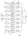
- FIG. 1 shows an overall example of processing modules of a programmable structure according to the invention adapted to the field of telephone transmissions.
- This set of modules includes a set of programmable filters (FILT) 10, a set of power estimation modules (PWR) 20, a set of modules 30 providing a value threshold VT, and a set of comparators (COMP) 32.
- An example programmable filter 10 and power estimation module 20 will be described later.
- FIG 1 there is shown eight modules, numbered 0 to 7, of each type.
- the exits comparators 32, providing detection signals of DET tone, are stored in a register (latch) 34.
- the digital signal to be processed Rx is available in a module 36, which is, for example, a register updated at the frequency sampling signal Rx.
- a value corresponding to GND ground potential is available in a module 38, which is, for example, made up of a set of bits forced into permanence to mass potential.
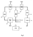
- FIG. 2 shows schematically a programmable structure according to the invention. Filters 10 and power estimators 20 are gathered in a block 50. The comparators 32 are gathered in a block 52.
- each signal is assigned, according to the invention, of a fixed address of a location of a signal memory 54.
- the address 00h (where the letter h means that the number is hexadecimal) at zero signal GND
- address 01h at signal input Rx addresses 10 a.m. to 5 p.m. at the outputs of filters 10, the addresses 8 p.m. to 7 p.m. at the outputs of the power estimators 20, and the addresses 30h to 37h at the threshold values VT.
- the locations of memory 54 are updated, to each sampling period, by the corresponding values of the outputs of the modules 50 and of the input signal Rx.
- the VT threshold values are written to their respective locations of memory 54, initially, for example at power up of the structure.
- the inputs of the modules 50 are associated respectively at fixed locations in a programming memory 56.
- a user writes (program) the address of the signal he wishes to apply to the module entry associated with the slot.
- each input of the comparators 52 is associated with a respective fixed location of a memory of programming 58 in which the user writes the addresses signals to provide to the comparators.
- Each input of the modules 50 is also associated with a respective fixed location of an input memory 60 in which we write the values to provide to modules 50.
- each input of the comparators 52 is associated with a location respective fixed of an input memory 62 in which one writes the values of the signals to be supplied to the comparators 52.
- a control circuit 64 manages the transfers between the different memories, as described below.
- the modules 50 perform their operations using values memory 60 and the results are transferred to the respective addresses in memory 54.
- the comparators 52 carry out the comparisons from the respective values stored in memory 62, and validate or not the respective bits of register 34 ( Figure 1).
- each address stored in memory 56 is examined and the value stored at this address in memory 54 is transferred to a corresponding location in memory 60. Readings in memory 56 are carried out in the same order that the entries in memory 60 so as to respect the correspondence between the locations of memories 56 and 60 and the inputs of the modules 50.
- each address stored in memory 58 is examined and the value stored at this address in memory 54 is transferred to a corresponding location in memory 62.
- the modules 50 and the comparators 52 carry out their operations with new values.
- Intermediate transfer of memory 54 to memories 60 and 62 realizes, according to one aspect of the invention, a delay in a sampling period which is used to avoid a drawback discussed below.
- the memories 60 and 62 are constituted by input registers modules 50 and 52.
- the signal memory 54 consists of output registers of modules 50, of registers containing the threshold values VT, and of the register containing the value to be processed of the Rx signal.
- the modules 50 are a set of modules operating in parallel or sequentially, or one or two elementary modules reprogrammed to perform sequentially the operations of all filtering and estimation modules power.
- the operations of modules 50 and 52 are performed in software and memories 54 to 62 form part of the same and single memory also storing programmable parameters filters and power estimators.
- FIGS. 3A and 3B show two examples of programming of interconnection between three modules MOD1 to MOD3.
- a signal S is, in the two cases of FIGS. 3A and 3B, processed successively by modules MOD1 to MOD3.
- MOD1 and MOD2 provide intermediate results R1 and R2, and the MOD3 module provides the final R3 result.
- module operations do not are not performed simultaneously. Especially if these operations are performed in software, they are performed sequentially.
- Figures 3A and 3B we have shown from top to bottom the modules in order of execution of their operations. In FIG. 3A, the operations are carried out in the order of modules MOD1 to MOD3, and in the figure 3B, they are carried out in the order of modules MOD3 to MOD1.
- FIGS. 4A and 4B illustrate, for the configurations of FIGS. 3A and 3B respectively, an example of evolution of the signals S and R1 to R3 in the order of execution of the operations of the modules MOD1 to MOD3.
- a sample of the signal S is provided at an instant t 0 . It is assumed, for simplicity, that each of the modules MOD1 to MOD3 is such that it transmits at its output the value present at its input when the operation of the module is carried out.
- each module performs its operation at a time when the previous module has supplied its result, that is to say that a module of FIG. 3A performs its operation when its entry is at value expected.
- the sample from input signal S is transmitted to output R3 without delay (except that of module operations, which is neglected).
- the operation of a module is performed while that of the previous module has not yet been.
- the input of the module considered is not at the expected value, except for the MOD1 module.
- the sample of the signal S is transmitted on the output R1.
- the operations of the MOD3 and MOD2 modules are carried out from time t 0 but before that of the MOD1 module; the outputs R3 and R2 are in any states,
- the operation of the module MOD2 is carried out while its input (R1) receives the sample of the signal S. This sample is transmitted on the output R2.
- the operation of the MOD3 module is carried out before that of the MOD2 module; the output R3 is in any state.
- the operation of the MOD3 module is carried out while the sample is present at the input (R2) of the MOD3 module; this sample is transmitted to output R3.
- one aspect of the invention is to introduce a delay of a sampling period in each module.
- FIGS. 5A and 5B respectively illustrate the behaviors thus obtained in the cases of FIGS. 3A and 3B.
- FIG. 5A illustrating the behavior of the configuration of FIG. 3A
- the sample of the signal S is successively transmitted to the outputs R1 to R3 with a delay of a sampling period at each transmission.
- the output R3 provides the sample at an instant t 3 following the instant t 0 of three sampling periods.
- FIG. 5B illustrating the behavior of the configuration of FIG. 3B, the same phenomenon as that described with the aid of FIG. 4B occurs, but with a delay sampling period. It follows that the transmitted sample is found on the output R3 at time t 3 , as in FIG. 5A. Thus, whatever the connection order of the modules, the signals are transmitted with the same delay.
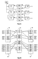
- FIGS 6A and 6B illustrate a programming example structure and corresponding contents of memories 54 to 62.
- the Rx signal, stored at address 01h in memory 54 is connected to filters 0 and 1 as well as to the power estimator 1.
- the locations of memory 56 associated with the filters 0 and 1 and to the power estimator 1 contain the address 01h.
- the output signal of filter 0, stored at address 10h in memory 54 is connected to the power estimator 0; the address 10h is stored in memory 56 at the location associated with the power estimator 0.
- the output signal from the filter 1, stored at address 11h in memory 54, is linked to filter 2; the address 11h is stored in memory 56 at the location associated with filter 2.
- the filter output signal 2, stored at the address 12h in memory 54, is connected to the power estimator 2; memory location 56 associated with the power estimator 2 contains the address 12h.
- the output signals of the power estimators 0 and 1, stored at addresses 8 p.m. and 9 p.m. in memory 54, are linked respectively to the first inputs (+) of the comparators 0 and 1, and the threshold values VT0 and VT1, stored at addresses 30h and 31h in memory 54, are provided respectively to the second inputs (-) of the comparators 0 and 1; the memory 58 stores the addresses 8 p.m. and 9 p.m. in locations associated with the first inputs of comparators 0 and 1, and stores the addresses 30h and 31h in locations associated with second inputs of comparators 0 and 1.
- the output signals power estimators 2 and 1 are provided respectively at the two comparator 2 inputs.
- the addresses 22h and 21h are stored in memory 58 at the locations associated with comparator inputs 2.
- the locations of the memories 60 and 62 are associated with the modules in the same order than the locations of programming memories 56 and 58.
- a each sample of the signal to be processed Rx, the addresses contained in programming memories 56 and 58 are read consecutively and the values contained at these addresses in the memory 54 are written in the same order in the memories input 60 and 62. So, for example, the Rx value contained in the address 01h from memory 54 is transferred to memory 60 the locations associated with filters 0 and 1 and the estimator of power 1.
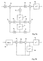
- Figures 7A and 7B show respective examples a filtering module and an estimation module of power.
- the filter module of FIG. 7A is a second order filter comprising two delay elements Z -1 70 and 71 arranged in series.
- the module 70 receives the output of an adder 72 via a multiplier by 2 73.
- a first input of the adder 72 receives the input signal from the filter via a multiplier 74 by a programmable coefficient C0.
- a second input of the adder 72 receives the output of an adder 75.
- the adder 75 receives on a first input the output of the delay element 71 via a multiplier 76 by a programmable coefficient C4 and on a second input the output of the delay element 70 via a multiplier 78 by a programmable coefficient C5.
- the outputs of the delay elements 70 and 71 are respectively supplied to the inputs of an adder 79 respectively via a multiplier 80 by a programmable coefficient C2 and a multiplier 81 by a programmable coefficient C1.
- the output of the adder 79 is supplied to a first input of an adder 82 which receives on a second input the output of the adder 72 via a multiplier 83 by a programmable coefficient C3.
- the output of the filter consists of the output of the adder 82.
- a delay element 84 connected to this output corresponds to the delay introduced according to the invention to avoid the drawback mentioned in connection with FIGS. 3A to 4B.
- the power estimator module shown in FIG. 7B comprises an element for calculating absolute value 86 which receives input from the module.
- Subtractor 87 provides the difference between the output of element 86 and an element of delay 88. This difference is supplied to an adder 89 by through a multiplier 90 by a programmable coefficient P1.
- the output of the adder 89, which constitutes the module output, is looped back to the second input of the adder 89 by the delay element 88.
- An element of delay 91 is arranged at the output of the module to obtain the delay avoiding the aforementioned drawback.
Landscapes
- Engineering & Computer Science (AREA)
- Computer Networks & Wireless Communication (AREA)
- Complex Calculations (AREA)
- Telephonic Communication Services (AREA)
- Cable Transmission Systems, Equalization Of Radio And Reduction Of Echo (AREA)
Description
Claims (6)
- Circuit de détection de signaux d'identification. dans un signal numérique d'entrée (Rx) qui présente des valeurs arrivant à une fréquence d'échantillonnage, comprenant un ensemble de modules de traitement (50) caractérisé en ce qu'il comprend en outre :une mémoire de signal (54) couplée aux modules de traitement (50), mise à jour à la fréquence d'échantillonnage du signal d'entrée, contenant les valeurs des signaux de sortie des modules de traitement et du signal d'entrée à des adresses associées ;une mémoire de programmation (56) couplée à la mémoire de signal (54) et aux modules de traitement (50), librement programmable par un utilisateur, contenant, à des emplacements associés aux entrées des modules de traitement, les adresses de la mémoire de signal associées aux signaux que l'utilisateur désire connecter auxdites entrées ; etdes moyens de commande (64) pour lire les adresses stockées dans la mémoire de programmation (56), lire les valeurs se trouvant à ces adresses dans la mémoire de signal (54), et fournir les valeurs lues aux entrées des modules de traitement dans un ordre correspondant aux emplacements de la mémoire de programmation.
- Circuit de détection selon la revendication 1, caractérisé en ce qu'il comprend une mémoire d'entrée (60, 62) dans laquelle les valeurs lues sont stockées à des emplacements associés respectivement aux entrées des modules de traitement.
- Circuit de détection selon la revendication 1, caractérisé en ce que les modules de traitement comprennent des premiers modules de traitement (50) et des deuxièmes modules de traitement (52) auxquels sont associés respectivement une première mémoire de programmation (56) et une deuxième mémoire de programmation (58), les moyens de commande (64) étant prévus pour lire les adresses stockées dans les première et deuxième mémoires de programmation à des fréquences différentes, lire les valeurs se trouvant à ces adresses dans la mémoire de signal (54), et fournir ces valeurs lues aux entrées des premiers modules de traitement (50) et des deuxièmes modules de traitement (52) dans des ordres respectifs correspondant aux emplacements des première et deuxième mémoires de programmation.
- Circuit de détection selon la revendication 3, caractérisé en ce qu'il comprend des première (60) et deuxième (62) mémoires d'entrée associées respectivement aux premiers modules de traitement (50) et aux deuxièmes modules de traitement (52), dans lesquelles les valeurs lues sont stockées à des emplacements associés respectivement aux entrées des premiers modules de traitement et des deuxièmes modules de traitement.
- Circuit de détection selon la revendication 3, caractérisé en ce que les premiers modules de traitement (50) comprennent des filtres programmables (10) et des modules de redressement et d'intégration (20), en ce que les deuxièmes modules de traitement (52) comprennent des comparateurs (32), et en ce que la mémoire de signal stocke en outre des valeurs seuil (VT) que l'utilisateur peut choisir de fournir à des comparateurs.
- Circuit de détection selon la revendication 1, caractérisé en ce que les opérations des modules de traitement sont effectuées par un ensemble programmable pour effectuer les opérations séquentiellement.
Applications Claiming Priority (2)
| Application Number | Priority Date | Filing Date | Title |
|---|---|---|---|
| FR9406724A FR2720577B1 (fr) | 1994-05-27 | 1994-05-27 | Circuit de détection de tonalité téléphonique. |
| FR9406724 | 1994-05-27 |
Publications (2)
| Publication Number | Publication Date |
|---|---|
| EP0689366A1 EP0689366A1 (fr) | 1995-12-27 |
| EP0689366B1 true EP0689366B1 (fr) | 2002-09-25 |
Family
ID=9463781
Family Applications (1)
| Application Number | Title | Priority Date | Filing Date |
|---|---|---|---|
| EP95410049A Expired - Lifetime EP0689366B1 (fr) | 1994-05-27 | 1995-05-23 | Circuit de détection de tonalité téléphonique |
Country Status (5)
| Country | Link |
|---|---|
| US (1) | US5659606A (fr) |
| EP (1) | EP0689366B1 (fr) |
| JP (1) | JPH0851487A (fr) |
| DE (1) | DE69528317D1 (fr) |
| FR (1) | FR2720577B1 (fr) |
Families Citing this family (5)
| Publication number | Priority date | Publication date | Assignee | Title |
|---|---|---|---|---|
| US5802112A (en) * | 1996-01-16 | 1998-09-01 | Transcendat Inc. | Multi-level, multi-frequency interference pattern analog waveform encoding of digital data for transmission |
| CN1101634C (zh) * | 1996-01-26 | 2003-02-12 | 皇家菲利浦电子有限公司 | 具有改善的单音检测的传输系统 |
| US6038262A (en) * | 1998-06-09 | 2000-03-14 | Transcendata, Inc. | Method and apparatus for compensation of electro-magnetic distortion using weighted feedback delay for amplitude coded sinusoidal waveform generation and transmission |
| US6937717B2 (en) * | 2001-03-29 | 2005-08-30 | Agere Systems Inc. | Low power signal detection |
| US20030081756A1 (en) * | 2001-10-23 | 2003-05-01 | Chan Norman C. | Multi-detector call classifier |
Citations (1)
| Publication number | Priority date | Publication date | Assignee | Title |
|---|---|---|---|---|
| GB2255472A (en) * | 1991-04-30 | 1992-11-04 | Rockwell International Corp | Telecommunication data analysis and transmission |
Family Cites Families (23)
| Publication number | Priority date | Publication date | Assignee | Title |
|---|---|---|---|---|
| US4354248A (en) * | 1979-11-28 | 1982-10-12 | Motorola, Inc. | Programmable multifrequency tone receiver |
| US4635250A (en) * | 1984-04-13 | 1987-01-06 | International Business Machines Corporation | Full-duplex one-sided cross-point switch |
| US4626629A (en) * | 1984-12-14 | 1986-12-02 | Gte Communication Systems Corporation | Digital multifrequency signal receiver |
| US4718057A (en) * | 1985-08-30 | 1988-01-05 | Advanced Micro Devices, Inc. | Streamlined digital signal processor |
| US4709344A (en) * | 1985-10-02 | 1987-11-24 | Motorola, Inc. | Programmable multifrequency digital tone receiver |
| US4908825A (en) * | 1988-04-08 | 1990-03-13 | Northern Telecom Limited | Memory organization and output sequencer for a signal processor |
| US5072217A (en) * | 1989-10-31 | 1991-12-10 | International Business Machines Corporation | One-sided crosspoint switch with distributed control |
| US5113431A (en) * | 1989-10-31 | 1992-05-12 | At&T Bell Laboratories | Distributed control teleconferencing voice bridge |
| JP2701513B2 (ja) * | 1990-03-29 | 1998-01-21 | 日本電気株式会社 | 回線切替制御方式 |
| US5325425A (en) * | 1990-04-24 | 1994-06-28 | The Telephone Connection | Method for monitoring telephone call progress |
| DE4017027A1 (de) * | 1990-05-26 | 1991-11-28 | Philips Patentverwaltung | Vermittlungssystem mit einer konferenzeinrichtung |
| US5420860A (en) * | 1990-06-18 | 1995-05-30 | Intelect, Inc. | Volume control for digital communication system |
| JPH04123621A (ja) * | 1990-09-14 | 1992-04-23 | Nippon Telegr & Teleph Corp <Ntt> | 反響消去装置 |
| US5255264A (en) * | 1991-09-26 | 1993-10-19 | Ipc Information Systems, Inc. | Distributed control switching network for multi-line telephone communications |
| FI89659C (fi) * | 1991-11-04 | 1993-10-25 | Nokia Telecommunications Oy | Foerfarande foer identifiering av en spaerrsignal hos en ekoslaeckare |
| JP3069419B2 (ja) * | 1991-11-27 | 2000-07-24 | ローム株式会社 | クロスポイントミキサ及びこれを備える電話機 |
| US5325427A (en) * | 1992-03-23 | 1994-06-28 | At&T Bell Laboratories | Apparatus and robust method for detecting tones |
| US5353342A (en) * | 1992-12-08 | 1994-10-04 | Bell Communications Research, Inc. | Adaptive multitone signaling method |
| JPH06318885A (ja) * | 1993-03-11 | 1994-11-15 | Nec Corp | 帯域分割適応フィルタによる未知システム同定の方法及び装置 |
| US5353348A (en) * | 1993-05-14 | 1994-10-04 | Jrc International, Inc. | Double echo cancelling system |
| US5363443A (en) * | 1993-12-08 | 1994-11-08 | At&T Bell Laboratories | Differing frequency sine wave generation from a look-up table |
| US5416836A (en) * | 1993-12-17 | 1995-05-16 | At&T Corp. | Disconnect signalling detection arrangement |
| US5533112A (en) * | 1994-03-31 | 1996-07-02 | Intel Corporation | Volume control in digital teleconferencing |
-
1994
- 1994-05-27 FR FR9406724A patent/FR2720577B1/fr not_active Expired - Fee Related
-
1995
- 1995-05-23 DE DE69528317T patent/DE69528317D1/de not_active Expired - Lifetime
- 1995-05-23 EP EP95410049A patent/EP0689366B1/fr not_active Expired - Lifetime
- 1995-05-24 US US08/449,120 patent/US5659606A/en not_active Expired - Lifetime
- 1995-05-25 JP JP7149798A patent/JPH0851487A/ja active Pending
Patent Citations (1)
| Publication number | Priority date | Publication date | Assignee | Title |
|---|---|---|---|---|
| GB2255472A (en) * | 1991-04-30 | 1992-11-04 | Rockwell International Corp | Telecommunication data analysis and transmission |
Also Published As
| Publication number | Publication date |
|---|---|
| JPH0851487A (ja) | 1996-02-20 |
| EP0689366A1 (fr) | 1995-12-27 |
| FR2720577A1 (fr) | 1995-12-01 |
| US5659606A (en) | 1997-08-19 |
| FR2720577B1 (fr) | 1996-08-14 |
| DE69528317D1 (de) | 2002-10-31 |
Similar Documents
| Publication | Publication Date | Title |
|---|---|---|
| FR2588980A1 (fr) | Processeur de traitement de signal numerique comportant plusieurs multiplicateurs | |
| EP0112761B1 (fr) | Dispositif de création sonore | |
| EP0046708B1 (fr) | Circuit de traitement numérique en arithmétique distribuée utilisant des multiplexeurs à l'entrée d'une mémoire | |
| FR2687814A1 (fr) | Processeur neuronal a cellules synaptiques reparties. | |
| FR2697663A1 (fr) | Circuit de test de mémoire. | |
| FR2588981A1 (fr) | Processeur de traitement de signal numerique | |
| EP0683454B1 (fr) | Procédé pour tester le déroulement d'un programme d'instructions | |
| EP0171856A1 (fr) | Processeur pour le traitement de signal et structure de multitraitement hiérarchisée comportant au moins un tel processeur | |
| EP0689366A1 (fr) | Circuit de détection de tonalité téléphonique | |
| FR2747528A1 (fr) | Structure de dispositif de banc de filtres numeriques et son procede de fonctionnement | |
| EP0733975B1 (fr) | Interface de sortie de données binaires | |
| EP0683455B1 (fr) | Circuit intégré comprenant des moyens pour arrêter l'exécution d'un programme d'instructions quand une combinaison de points d'arrêt est vérifiée | |
| EP0732809B1 (fr) | Dispositif de filtrage digital | |
| EP2215552B1 (fr) | Circuit comportant une machine microprogrammee pour traiter les entrees ou les sorties d'un processeur afin de les faire entrer ou sortir du circuit selon n'importe quel protocole de communication | |
| EP0585434B1 (fr) | Procede et dispositif de filtrage pour la reduction des preechos d'un signal audio-numerique | |
| EP0242258A1 (fr) | Dispositif de mise en oeuvre d'un algorithme dit de LEROUX- GUEGUEN,pour le codage d'un signal par prédiction linéaire | |
| EP1803061A1 (fr) | Systeme de processeur parallele reconfigurable, modulaire et hierarchique | |
| EP0112427A1 (fr) | Dispositif de commande logique programmable | |
| CH633922A5 (en) | Digital filter and use thereof in a voice-synthesis device | |
| EP0615374B1 (fr) | Procédé et dispositif de traitement d'écho entre deux voies de transmission présentant entre elles un couplage | |
| FR2541795A1 (fr) | Processeur universel, en particulier pour traitement de signal | |
| EP0046121A2 (fr) | Perfectionnements apportés aux filtres numériques et application de tels filtres numériques à la démodulation | |
| FR2897174A1 (fr) | Processeur comportant une interface de debogage integree controlee par l'unite de traitement du processeur | |
| EP0104290A1 (fr) | Processeur numérique de signal en temps réel | |
| FR2581469A1 (fr) | Dispositif d'entree-sortie vocale et installation a reconnaissance ou synthese de parole en comportant application |
Legal Events
| Date | Code | Title | Description |
|---|---|---|---|
| PUAI | Public reference made under article 153(3) epc to a published international application that has entered the european phase |
Free format text: ORIGINAL CODE: 0009012 |
|
| AK | Designated contracting states |
Kind code of ref document: A1 Designated state(s): DE FR GB IT |
|
| 17P | Request for examination filed |
Effective date: 19960607 |
|
| RAP3 | Party data changed (applicant data changed or rights of an application transferred) |
Owner name: STMICROELECTRONICS S.A. |
|
| 17Q | First examination report despatched |
Effective date: 20010115 |
|
| GRAG | Despatch of communication of intention to grant |
Free format text: ORIGINAL CODE: EPIDOS AGRA |
|
| RAP1 | Party data changed (applicant data changed or rights of an application transferred) |
Owner name: STMICROELECTRONICS S.A. |
|
| GRAG | Despatch of communication of intention to grant |
Free format text: ORIGINAL CODE: EPIDOS AGRA |
|
| GRAH | Despatch of communication of intention to grant a patent |
Free format text: ORIGINAL CODE: EPIDOS IGRA |
|
| GRAH | Despatch of communication of intention to grant a patent |
Free format text: ORIGINAL CODE: EPIDOS IGRA |
|
| GRAA | (expected) grant |
Free format text: ORIGINAL CODE: 0009210 |
|
| AK | Designated contracting states |
Kind code of ref document: B1 Designated state(s): DE FR GB IT |
|
| PG25 | Lapsed in a contracting state [announced via postgrant information from national office to epo] |
Ref country code: IT Free format text: LAPSE BECAUSE OF FAILURE TO SUBMIT A TRANSLATION OF THE DESCRIPTION OR TO PAY THE FEE WITHIN THE PRE;WARNING: LAPSES OF ITALIAN PATENTS WITH EFFECTIVE DATE BEFORE 2007 MAY HAVE OCCURRED AT ANY TIME BEFORE 2007. THE CORRECT EFFECTIVE DATE MAY BE DIFFERENT FROM THE ONE RECORDED.SCRIBED TIME-LIMIT Effective date: 20020925 |
|
| REG | Reference to a national code |
Ref country code: GB Ref legal event code: FG4D Free format text: NOT ENGLISH |
|
| REF | Corresponds to: |
Ref document number: 69528317 Country of ref document: DE Date of ref document: 20021031 |
|
| PG25 | Lapsed in a contracting state [announced via postgrant information from national office to epo] |
Ref country code: DE Free format text: LAPSE BECAUSE OF FAILURE TO SUBMIT A TRANSLATION OF THE DESCRIPTION OR TO PAY THE FEE WITHIN THE PRESCRIBED TIME-LIMIT Effective date: 20021228 |
|
| GBT | Gb: translation of ep patent filed (gb section 77(6)(a)/1977) |
Effective date: 20030128 |
|
| PLBE | No opposition filed within time limit |
Free format text: ORIGINAL CODE: 0009261 |
|
| STAA | Information on the status of an ep patent application or granted ep patent |
Free format text: STATUS: NO OPPOSITION FILED WITHIN TIME LIMIT |
|
| 26N | No opposition filed |
Effective date: 20030626 |
|
| PGFP | Annual fee paid to national office [announced via postgrant information from national office to epo] |
Ref country code: FR Payment date: 20050511 Year of fee payment: 11 |
|
| PGFP | Annual fee paid to national office [announced via postgrant information from national office to epo] |
Ref country code: GB Payment date: 20050518 Year of fee payment: 11 |
|
| PG25 | Lapsed in a contracting state [announced via postgrant information from national office to epo] |
Ref country code: GB Free format text: LAPSE BECAUSE OF NON-PAYMENT OF DUE FEES Effective date: 20060523 |
|
| GBPC | Gb: european patent ceased through non-payment of renewal fee |
Effective date: 20060523 |
|
| REG | Reference to a national code |
Ref country code: FR Ref legal event code: ST Effective date: 20070131 |
|
| PG25 | Lapsed in a contracting state [announced via postgrant information from national office to epo] |
Ref country code: FR Free format text: LAPSE BECAUSE OF NON-PAYMENT OF DUE FEES Effective date: 20060531 |