EP0692149B1 - Elektrischer verbinder - Google Patents
Elektrischer verbinder Download PDFInfo
- Publication number
- EP0692149B1 EP0692149B1 EP94912920A EP94912920A EP0692149B1 EP 0692149 B1 EP0692149 B1 EP 0692149B1 EP 94912920 A EP94912920 A EP 94912920A EP 94912920 A EP94912920 A EP 94912920A EP 0692149 B1 EP0692149 B1 EP 0692149B1
- Authority
- EP
- European Patent Office
- Prior art keywords
- peg
- circuit board
- electrical connector
- metal ring
- housing body
- Prior art date
- Legal status (The legal status is an assumption and is not a legal conclusion. Google has not performed a legal analysis and makes no representation as to the accuracy of the status listed.)
- Expired - Lifetime
Links
Images


Classifications
-
- H—ELECTRICITY
- H01—ELECTRIC ELEMENTS
- H01R—ELECTRICALLY-CONDUCTIVE CONNECTIONS; STRUCTURAL ASSOCIATIONS OF A PLURALITY OF MUTUALLY-INSULATED ELECTRICAL CONNECTING ELEMENTS; COUPLING DEVICES; CURRENT COLLECTORS
- H01R12/00—Structural associations of a plurality of mutually-insulated electrical connecting elements, specially adapted for printed circuits, e.g. printed circuit boards [PCB], flat or ribbon cables, or like generally planar structures, e.g. terminal strips, terminal blocks; Coupling devices specially adapted for printed circuits, flat or ribbon cables, or like generally planar structures; Terminals specially adapted for contact with, or insertion into, printed circuits, flat or ribbon cables, or like generally planar structures
- H01R12/50—Fixed connections
- H01R12/51—Fixed connections for rigid printed circuits or like structures
- H01R12/55—Fixed connections for rigid printed circuits or like structures characterised by the terminals
- H01R12/57—Fixed connections for rigid printed circuits or like structures characterised by the terminals surface mounting terminals
-
- H—ELECTRICITY
- H01—ELECTRIC ELEMENTS
- H01R—ELECTRICALLY-CONDUCTIVE CONNECTIONS; STRUCTURAL ASSOCIATIONS OF A PLURALITY OF MUTUALLY-INSULATED ELECTRICAL CONNECTING ELEMENTS; COUPLING DEVICES; CURRENT COLLECTORS
- H01R12/00—Structural associations of a plurality of mutually-insulated electrical connecting elements, specially adapted for printed circuits, e.g. printed circuit boards [PCB], flat or ribbon cables, or like generally planar structures, e.g. terminal strips, terminal blocks; Coupling devices specially adapted for printed circuits, flat or ribbon cables, or like generally planar structures; Terminals specially adapted for contact with, or insertion into, printed circuits, flat or ribbon cables, or like generally planar structures
- H01R12/70—Coupling devices
- H01R12/71—Coupling devices for rigid printing circuits or like structures
- H01R12/72—Coupling devices for rigid printing circuits or like structures coupling with the edge of the rigid printed circuits or like structures
- H01R12/722—Coupling devices for rigid printing circuits or like structures coupling with the edge of the rigid printed circuits or like structures coupling devices mounted on the edge of the printed circuits
- H01R12/724—Coupling devices for rigid printing circuits or like structures coupling with the edge of the rigid printed circuits or like structures coupling devices mounted on the edge of the printed circuits containing contact members forming a right angle
-
- H—ELECTRICITY
- H01—ELECTRIC ELEMENTS
- H01R—ELECTRICALLY-CONDUCTIVE CONNECTIONS; STRUCTURAL ASSOCIATIONS OF A PLURALITY OF MUTUALLY-INSULATED ELECTRICAL CONNECTING ELEMENTS; COUPLING DEVICES; CURRENT COLLECTORS
- H01R12/00—Structural associations of a plurality of mutually-insulated electrical connecting elements, specially adapted for printed circuits, e.g. printed circuit boards [PCB], flat or ribbon cables, or like generally planar structures, e.g. terminal strips, terminal blocks; Coupling devices specially adapted for printed circuits, flat or ribbon cables, or like generally planar structures; Terminals specially adapted for contact with, or insertion into, printed circuits, flat or ribbon cables, or like generally planar structures
- H01R12/70—Coupling devices
- H01R12/71—Coupling devices for rigid printing circuits or like structures
- H01R12/72—Coupling devices for rigid printing circuits or like structures coupling with the edge of the rigid printed circuits or like structures
- H01R12/722—Coupling devices for rigid printing circuits or like structures coupling with the edge of the rigid printed circuits or like structures coupling devices mounted on the edge of the printed circuits
- H01R12/727—Coupling devices presenting arrays of contacts
-
- H—ELECTRICITY
- H05—ELECTRIC TECHNIQUES NOT OTHERWISE PROVIDED FOR
- H05K—PRINTED CIRCUITS; CASINGS OR CONSTRUCTIONAL DETAILS OF ELECTRIC APPARATUS; MANUFACTURE OF ASSEMBLAGES OF ELECTRICAL COMPONENTS
- H05K3/00—Apparatus or processes for manufacturing printed circuits
- H05K3/30—Assembling printed circuits with electric components, e.g. with resistors
- H05K3/306—Assembling printed circuits with electric components, e.g. with resistors with lead-in-hole components
-
- H—ELECTRICITY
- H05—ELECTRIC TECHNIQUES NOT OTHERWISE PROVIDED FOR
- H05K—PRINTED CIRCUITS; CASINGS OR CONSTRUCTIONAL DETAILS OF ELECTRIC APPARATUS; MANUFACTURE OF ASSEMBLAGES OF ELECTRICAL COMPONENTS
- H05K3/00—Apparatus or processes for manufacturing printed circuits
- H05K3/30—Assembling printed circuits with electric components, e.g. with resistors
- H05K3/32—Assembling printed circuits with electric components, e.g. with resistors electrically connecting electric components or wires to printed circuits
- H05K3/34—Assembling printed circuits with electric components, e.g. with resistors electrically connecting electric components or wires to printed circuits by soldering
- H05K3/3447—Lead-in-hole components
Definitions
- the present invention relates to an electrical connector and, in particular, to an electrical connector of a type solderable to a board such as a printed circuit board.
- a method, referred to in the art as "hot riveting", is known for fixing an electrical connector to a printed circuit board.
- the hot riveting method involves the use of a connector housing comprising a housing body made of plastic and a plastic peg (leg) downwardly extending from the lower surface of the housing body.
- the peg is inserted through a peg insertion bore in the printed circuit board until the lower surface of the housing body lies flat on the board surface. Then, the distal end of the peg, which protrudes from the insertion bore on the opposite side of the circuit board, is contacted with a mold taking surface of a heated mold pushing rod so as to melt and deform the peg.
- the mold taking surface of the mold pushing rod has a spherical recess with a greater diameter than that of the insertion bore in the board.
- the distal end of the peg is spherically deformed to a diameter greater than that of the insertion hole, thereby fixing the connector to the board.
- the peg does not always deform to the predetermined spherical shape of the mold taking surface due to the nonuniformity of heat conduction from the mold pushing rod to the peg or due to the non-uniformity, etc., of the inner mechanical properties of the peg resulting from the non-uniform hardness of the resin inside the peg.
- the housing-to-board connection force becomes unstable, thus posing a reliability problem.
- An object of the present invention is to provide an electrical connector which can readily and positively be fixed to a board, such as a printed circuit board, and can eliminate the necessity of providing any melting means, such as a mold pushing rod.
- US-A-4850902 describes an electrical connector with a housing for positioning on one side of a printed circuit board provided with a through hole.
- the housing is equipped with contact terminals and with a mounting post which passes through the hole and forms a snap-fit with the other side of the printed circuit board.
- the present invention is concerned with an electrical connector to be automatically soldered to a circuit board having a through hole, said electrical connector comprising:
- the invention provides a method of fixing an electrical connector to a circuit board wherein said connector comprises a housing body with a plurality of contact terminals arranged on the housing body and having a peg of plastics material projecting from a surface thereof and wherein said circuit board has a through hole for receiving the peg, said method comprising the steps of:
- the peg is soldered to the circuit board by means of a cylindrical metal ring fitted over the peg and through the through hole in the circuit board such that it occupies the space between the peg and the surface of the through hole.
- the solder means may comprise a solderable coating formed on the peg.
- the peg is soldered to the board during the same soldering step as the plurality of contact terminals.
- FIG. 1 shows an electrical connector 12 in accordance with one embodiment of the present invention.
- the electrical connector 12 comprises a receptacle connector (i.e., a female connector such as an outlet connector and socket) that is to be mounted on a main side 10a of a printed circuit board 10.
- a receptacle connector i.e., a female connector such as an outlet connector and socket
- the receptacle connector 12 is equipped with a receptacle housing made of an electrically insulating resin material and connectable to a male plug connector (not shown).
- the receptacle housing is equipped with a housing body 14 of substantially rectangular configuration.
- the housing body 14 has a rod-like peg 16 formed integral with the housing body 14.
- a front part of the lower surface 14a of the housing body 14 extends past an edge of the board 10, while the remaining portion of the lower surface 14a of the housing body 14 lies flat on the main side 10a of the board 10.
- a front wall 14b of the housing body 14 is situated substantially perpendicular to the lower surface 14a.
- the front wall 14b has openings 18 communicating with the -inside of the body 14.
- Solder tails 26, described hereinafter in greater detail, are projected from a rear wall 14c of the housing body 14.
- a plurality of receptacle contacts 20 are arranged in corresponding openings 18.
- the receptacle contacts 20 have receptacle sections 22 for receiving plug contacts (not shown) of a male contact member (not shown) via the front wall 14b of the housing 14.
- the receptacle sections 22 may be designed so as to correspond to the configuration of the plug contacts, and are not restricted to the particular configuration shown.
- Each receptacle contact 20 further has a solder tail 26 that inserts into, and is subsequently soldered to, a corresponding through hole 24 of a circuit pattern on the printed circuit board 10.
- the peg 16 projects vertically from the lower surface 14a of the housing body 14 and extends through an insertion hole 28.
- the distal end of the peg 16 protrudes outward from the hole 28 on the opposite, solder side 10b of the printed circuit board 10.
- an annular ring 30, which is made of a conductive material or a solderable material, is located around the peg insertion hole 28 on the solder side 10b of the board 10.
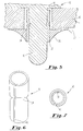
- a substantially cylindrical metal ring 32 is fitted over the peg 16. A portion of the cylindrical metal ring 32 extends into the peg insertion hole 28 so as to be disposed between the peg 16 and the annular surface of the hole 28.
- annular projection 34 is formed on the inner surface of the cylindrical metal ring 32 and extends toward the center axis of the cylindrical metal ring. It is desirable that the cross-sectional configuration of the annular projection 34 be, for example, V-shaped or wedge-shaped and have a projected end oriented toward the center axis of the cylindrical metal ring 32.
- the cylindrical metal ring 32 has an outer diameter of a size insertable into the peg insertion hole 28.
- the inner diameter of the cylindrical metal ring 32 is of such a size as to allow the metal ring to be fitted over the peg 16.
- the inner diameter of the cylindrical metal ring 32 is made smaller than the outer diameter of the peg 16.
- the area of the annular projection 34 on the cylindrical metal ring 32 receives a radial expansion force from the outer periphery of the peg 16 which acts against the normal tendency of the metal ring 32 to return, under its own elasticity, back to its original state.
- the annular projection 34 bites into the peg 16 and hence the peg 16 is held in place.
- the cylindrical metal ring 32 is fixed in place on the peg 16 and will not drop off the peg 16 under any slight oscillation or external force. If the cross-sectional shape of the annular projection is so formed as to have a pointed end as in the present embodiment, then the pointed end of the annular projection bites more forcibly into the peg 16, thus enabling it to be more firmly secured to the peg 16.
- FIGS. 4 and 5 show the receptacle connector 12 in a soldering bath at an automatic soldering station.
- the solder tails 26 of the contacts 20 are inserted through the corresponding through holes 24 in the board 10 and the metal ring 32 is fitted over the peg 16.
- the solder side 10b of the board 10 is exposed to a molten solder wave 36 jetted in a wavy manner.
- the solder wave 36 By action of the solder wave 36, the solder tails 26 are soldered to their corresponding through holes 24.
- a solder connection area 38 (Fig. 5) is formed between the angular ring 30 on the solder side 10b of the board 10 and the metal ring 32, thereby soldering the two together.
- the peg 16 being made of a resin material, is softened by heat (about 250 to 260°C) from the solder wave 36.
- the annular projection 34 on the inner surface of the metal ring 32 bites more forcibly into the peg 16, thus fixing the metal ring 32 to the peg 16 with a stronger force.
- the soldering of the annular ring 30 to the metal ring 32 firmly fixes the connector 12 to the board 10.
- FIGS. 6 and 7 show a second embodiment of the present invention.
- This embodiment is similar to the first embodiment except that the structure of the metal ring 32 is different.
- the metal ring 32 has a slit 40 along its axial direction. The slit 40 allows the metal ring 32 to expand more easily in the radial direction, thus facilitating the fitting of the metal ring 32 over the peg 16.
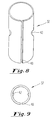
- FIGS. 8 and 9 show a third embodiment of the present invention.
- the third embodiment differs from the first embodiment in that the metal ring 32 of the third embodiment has a plurality of projections 42, in place of the aforementioned annular projection 34, which are provided at given intervals along the inner wall of the metal ring 32. It is preferred that the cross-sectional shape of each projection 42 have a pointed end projected toward the center axis of the metal ring 32, such as a V-shaped or wedge-like end. Further a slit 40 may be provided as in the case of the second embodiment.
- the receptacle connector 12 is fixed to the board 10 mainly by the metal ring 32, and the design tolerance can be more lenient for the peg 16. It is therefore easy to mold the housing body 14 integral with the peg 16.
- the peg 16 it may be possible to solder the peg 16 directly to the annular ring 30 of the board 10, instead of interposing the metal ring 32, by partially coating the peg 16 with a material with which the peg 16 can be soldered. Or it may be possible to manufacture the peg 16 itself from a solderable material. In this case, the housing body 14 and peg 16 are connected together by a proper method in place of being formed integral with each other. In the case where the peg 16 is made of a conductive material, it is of course necessary to electrically insulate the contacts 20 and peg 16 from each other. In any case, the softening of the peg 16 is achieved automatically by the soldering operation, and therefore, it is not necessary to use any melting means such as a conventional mold pushing rod.
- the present invention is not restricted thereto.
- the present invention can be applied to an electrical connector of any proper type necessary to be fixed to a board.
- the shapes of the housing body and contacts are not limited to those disclosed in the Figures, nor are the shapes of the metal ring 32, projections 34, 42 and slit 40. It is understood, therefore, that changes may be made to the embodiments described above without departing from the broad inventive concepts thereof. Accordingly, this invention is not limited to the particular embodiments disclosed, but is intended to cover all modifications that are within the scope and spirit of the invention as defined by the appended claims.
Landscapes
- Coupling Device And Connection With Printed Circuit (AREA)
- Multi-Conductor Connections (AREA)
- Structures For Mounting Electric Components On Printed Circuit Boards (AREA)
Claims (11)
- Elektrischer Verbinder (12) zum automatischen Anlöten an eine Leiterplatte (10) mit einem Durchgangsloch (28), wobei der elektrische Verbinder umfaßt:dadurch gekennzeichnet, daß der Stift (16) mit einem Lötmittel (32) versehen ist zum Festlegen des Stifts an der Leiterplatte während eines Lötschrittes, um dadurch den elektrischen Verbinder an der Leiterplatte zu fixieren.einen an einer Seite der Leiterplatte zu positionierenden Gehäusekörper (14),eine Mehrzahl von in dem Gehäusekörper angeordneten Kontaktanschlüssen (20, 26), undein Kunststoffstift (16), welcher von einer Oberfläche des Gehäusekörpers hervorsteht und dazu ausgebildet ist, durch das Durchgangsloch (28) an der Leiterplatte hindurchzuragen, wenn der Gehäusekörper an der einen Seite der Leiterplatte angeordnet ist,
- Elektrischer Verbinder (12) nach Anspruch 1, worin das Lötmittel ein elektrischer Metallring (32) ist, welcher zur Passung über den Stift (16) und durch das Durchgangsloch (28) hindurch ausgebildet ist, wenn der Gehäusekörper (14) an der Leiterplatte angeordnet ist, wobei der zylindrische Metallring (32) das Anlöten des Stifts an die entgegengesetzte Seite der Leiterplatte ermöglicht, um den elektrischen Verbinder an der Leiterplatte zu fixieren.
- Elektrischer Verbinder nach Anspruch 2, worin der zylindrische Metallring (32) einen entlang seiner axialen Richtung darin ausgebildeten Schlitz (40) aufweist, um das Passen des Metallrings über den Stift (16) zu erleichtern.
- Elektrischer Verbinder nach Anspruch 2 oder 3, worin der zylindrische Metallring (32) wenigstens einen an einer Innenoberfläche desselben ausgebildeten Vorsprung (34, 42) aufweist, wobei der wenigstens eine Vorsprung dazu ausgebildet ist, in den Stift (16) einzuschneiden, wenn der Metallring (32) über den Stift gepaßt ist, wodurch der Ring (32) an dem Stift (16) fixiert ist.
- Elektrischer Verbinder nach Anspruch 4, worin der wenigstens eine Vorsprung (34) einen um die Innenoberfläche des zylindrischen Rings herum ausgebildeten ringförmigen Vorsprung umfaßt.
- Elektrischer Verbinder nach Anspruch 4, worin der wenigstens eine Vorsprung (42) eine Mehrzahl von separaten Vorsprüngen umfaßt, welche um die Innenoberfläche des zylindrischen Metallrings (32) herum mit Abstand angeordnet sind.
- Elektrischer Verbinder nach Anspruch 4, 5 oder 6, worin der wenigstens eine Vorsprung (34, 42) V-förmig ist.
- Elektrischer Verbinder nach Anspruch 1, worin das Lötmittel eine an dem Stift gebildete lötbare Beschichtung umfaßt.
- Elektrischer Verbinder nach einem der Ansprüche 1 bis 8, worin der Stift (16) mit dem Gehäusekörper (14) integral ausgebildet ist.
- Verfahren zum Festlegen eines elektrischen Verbinders (12) an einer Leiterplatte (10), worin der Verbinder einen Gehäusekörper (14) mit einem Stift (16) aus Kunststoffmaterial umfaßt, welcher von einer Oberfläche desselben hervorsteht, und worin die Leiterplatte (10) ein Durchgangsloch (28) aufweist, worin das Verfahren die Schritte umfaßt:a) Positionieren des elektrischen Verbinders (12) an einer Seite der Leiterplatte (10) derart, daß der Stift (16) durch das Durchgangsloch (28) hindurchgeführt wird,b) Vorsehen eines lötbaren Mittels in der Form eines Metallrings (32) über dem Stift (16), undc) Durchführen eines Lötvorgangs an der entgegengesetzten Seite der Leiterplatte, wodurch der über den Stift (16) gepaßte Metallring (32) an die entgegengesetzte Seite der Leiterplatte angelötet wird, um dadurch den elektrischen Verbinder an der Leiterplatte zu fixieren.
- Verfahren nach Anspruch 10, worin der Metallring (32) einen zylindrischen Metallring mit einem darin entlang seiner axialen Richtung ausgebildeten Schlitz (40) und wenigstens einem Vorsprung (34, 42) umfaßt, welcher an einer Innenoberfläche desselben ausgebildet ist, und worin der Paß-Schritt das Plazieren des Metallrings (32) auf dem Stift (16) und das Pressen des Rings (32) auf den Stift (16) umfaßt, so daß der Vorsprung (34) in den Ring (16) einschneidet.
Applications Claiming Priority (3)
| Application Number | Priority Date | Filing Date | Title |
|---|---|---|---|
| JP1993015919U JP2534861Y2 (ja) | 1993-03-31 | 1993-03-31 | 電気コネクタ結合装置 |
| JP15919/93 | 1993-03-31 | ||
| PCT/US1994/003560 WO1994023474A1 (en) | 1993-03-31 | 1994-03-31 | Electrical connector |
Publications (3)
| Publication Number | Publication Date |
|---|---|
| EP0692149A1 EP0692149A1 (de) | 1996-01-17 |
| EP0692149A4 EP0692149A4 (de) | 1996-11-27 |
| EP0692149B1 true EP0692149B1 (de) | 1999-06-02 |
Family
ID=11902192
Family Applications (1)
| Application Number | Title | Priority Date | Filing Date |
|---|---|---|---|
| EP94912920A Expired - Lifetime EP0692149B1 (de) | 1993-03-31 | 1994-03-31 | Elektrischer verbinder |
Country Status (6)
| Country | Link |
|---|---|
| EP (1) | EP0692149B1 (de) |
| JP (1) | JP2534861Y2 (de) |
| KR (1) | KR960702198A (de) |
| DE (1) | DE69418867T2 (de) |
| SG (1) | SG48095A1 (de) |
| WO (1) | WO1994023474A1 (de) |
Families Citing this family (6)
| Publication number | Priority date | Publication date | Assignee | Title |
|---|---|---|---|---|
| JPH10294142A (ja) * | 1997-04-18 | 1998-11-04 | Hirose Electric Co Ltd | 回路基板用電気コネクタ |
| DE102005016283A1 (de) * | 2005-04-08 | 2006-10-12 | Siemens Ag Österreich | Verfahren zur Befestigung von Bauteilen auf Schaltungsträgern |
| JP5532335B2 (ja) * | 2010-09-17 | 2014-06-25 | 住友電装株式会社 | 固定部材の接続構造及び固定部材 |
| GB2493754A (en) * | 2011-08-17 | 2013-02-20 | Vion Food Group Ltd | Curing composition comprising an umami flavouring agent |
| DE102014109220A1 (de) * | 2014-07-01 | 2016-01-07 | Endress + Hauser Gmbh + Co. Kg | Leiterplattenverbindungselement |
| US11826861B1 (en) * | 2020-08-12 | 2023-11-28 | Sion Power Corporation | Joining systems, clamping fixtures, and related systems and methods |
Family Cites Families (7)
| Publication number | Priority date | Publication date | Assignee | Title |
|---|---|---|---|---|
| US3932934A (en) * | 1974-09-16 | 1976-01-20 | Amp Incorporated | Method of connecting terminal posts of a connector to a circuit board |
| US4802862A (en) * | 1981-03-30 | 1989-02-07 | North American Specialties Corporation | Solderable electrical contact |
| US4583807A (en) * | 1983-12-13 | 1986-04-22 | Amp Incorporated | Surface mount connector |
| US5029748A (en) * | 1987-07-10 | 1991-07-09 | Amp Incorporated | Solder preforms in a cast array |
| US4850902A (en) * | 1988-04-11 | 1989-07-25 | Amp Incorporated | Electrical connector having improved characteristics for retaining leads to the connector housing and method of making the electrical connector |
| US4872846A (en) * | 1988-07-21 | 1989-10-10 | Clark Thomas C | Solder containing electrical connector and method for making same |
| JP2537459Y2 (ja) * | 1992-03-05 | 1997-06-04 | ヒロセ電機株式会社 | 電気コネクタの基板取付構造 |
-
1993
- 1993-03-31 JP JP1993015919U patent/JP2534861Y2/ja not_active Expired - Fee Related
-
1994
- 1994-03-31 DE DE69418867T patent/DE69418867T2/de not_active Expired - Fee Related
- 1994-03-31 KR KR1019950704212A patent/KR960702198A/ko not_active Ceased
- 1994-03-31 SG SG1996007009A patent/SG48095A1/en unknown
- 1994-03-31 EP EP94912920A patent/EP0692149B1/de not_active Expired - Lifetime
- 1994-03-31 WO PCT/US1994/003560 patent/WO1994023474A1/en not_active Ceased
Also Published As
| Publication number | Publication date |
|---|---|
| WO1994023474A1 (en) | 1994-10-13 |
| SG48095A1 (en) | 1998-04-17 |
| EP0692149A4 (de) | 1996-11-27 |
| JPH0673869U (ja) | 1994-10-18 |
| JP2534861Y2 (ja) | 1997-05-07 |
| EP0692149A1 (de) | 1996-01-17 |
| DE69418867T2 (de) | 1999-10-07 |
| DE69418867D1 (de) | 1999-07-08 |
| KR960702198A (ko) | 1996-03-28 |
Similar Documents
| Publication | Publication Date | Title |
|---|---|---|
| CA2267292C (en) | Low profile connector | |
| US6241535B1 (en) | Low profile connector | |
| US4195900A (en) | Terminal housing having improved mounting means | |
| US5616035A (en) | Electrical connector | |
| US20050106949A1 (en) | Housing for an electrical plug-in connector | |
| US6442036B2 (en) | Substrate mount type terminal | |
| US4797110A (en) | Printed circuit board with integral electrical connector and method for making it using wave soldering | |
| WO1994023474A1 (en) | Electrical connector | |
| JP3179006B2 (ja) | I/oコネクタの製造方法 | |
| EP0893843A1 (de) | Modularer koaxialer Verbinder | |
| US6083054A (en) | Bulb socket and method for manufacturing the same | |
| EP1039542B1 (de) | Verbindersatz | |
| EP0910877B1 (de) | Prezisionsgegossene zylinder | |
| JPH02216776A (ja) | 表面実装コネクタ | |
| US20020019168A1 (en) | Pin array header with floating surface mount interconnects | |
| EP1069650B1 (de) | Metallkontakt | |
| JPH051911Y2 (de) | ||
| US6290544B1 (en) | Electrical connector with adapter for increasing an overall height of the connector above a prited circuit borad | |
| US20040229503A1 (en) | Surface mounted electrical component | |
| EP0795938A1 (de) | Elektrischer Steckverbinder mit Montur, Steckverbinderanordnung und Methode zur Verbindermontage | |
| JPH09283223A (ja) | 電気コネクタ | |
| JP2000082517A (ja) | プレスフィット付きコンタクト | |
| EP0733273A1 (de) | Verbinder | |
| JPH0536763U (ja) | リードソケツト用インナーコンタクト | |
| JPH0625910Y2 (ja) | 基板実装コネクタの整列取付用治具 |
Legal Events
| Date | Code | Title | Description |
|---|---|---|---|
| PUAI | Public reference made under article 153(3) epc to a published international application that has entered the european phase |
Free format text: ORIGINAL CODE: 0009012 |
|
| 17P | Request for examination filed |
Effective date: 19951010 |
|
| AK | Designated contracting states |
Kind code of ref document: A1 Designated state(s): DE FR GB |
|
| RAP1 | Party data changed (applicant data changed or rights of an application transferred) |
Owner name: CONNECTOR SYSTEMS TECHNOLOGY N.V. Owner name: BERG ELECTRONICS MANUFACTURING B.V. |
|
| A4 | Supplementary search report drawn up and despatched |
Effective date: 19961009 |
|
| AK | Designated contracting states |
Kind code of ref document: A4 Designated state(s): DE FR GB |
|
| 17Q | First examination report despatched |
Effective date: 19970227 |
|
| GRAG | Despatch of communication of intention to grant |
Free format text: ORIGINAL CODE: EPIDOS AGRA |
|
| RAP1 | Party data changed (applicant data changed or rights of an application transferred) |
Owner name: BERG ELECTRONICS MANUFACTURING B.V. |
|
| GRAG | Despatch of communication of intention to grant |
Free format text: ORIGINAL CODE: EPIDOS AGRA |
|
| GRAG | Despatch of communication of intention to grant |
Free format text: ORIGINAL CODE: EPIDOS AGRA |
|
| GRAH | Despatch of communication of intention to grant a patent |
Free format text: ORIGINAL CODE: EPIDOS IGRA |
|
| GRAH | Despatch of communication of intention to grant a patent |
Free format text: ORIGINAL CODE: EPIDOS IGRA |
|
| GRAA | (expected) grant |
Free format text: ORIGINAL CODE: 0009210 |
|
| AK | Designated contracting states |
Kind code of ref document: B1 Designated state(s): DE FR GB |
|
| REF | Corresponds to: |
Ref document number: 69418867 Country of ref document: DE Date of ref document: 19990708 |
|
| ET | Fr: translation filed | ||
| PLBE | No opposition filed within time limit |
Free format text: ORIGINAL CODE: 0009261 |
|
| STAA | Information on the status of an ep patent application or granted ep patent |
Free format text: STATUS: NO OPPOSITION FILED WITHIN TIME LIMIT |
|
| 26N | No opposition filed | ||
| REG | Reference to a national code |
Ref country code: GB Ref legal event code: IF02 |
|
| PGFP | Annual fee paid to national office [announced via postgrant information from national office to epo] |
Ref country code: GB Payment date: 20030204 Year of fee payment: 10 |
|
| PGFP | Annual fee paid to national office [announced via postgrant information from national office to epo] |
Ref country code: FR Payment date: 20030303 Year of fee payment: 10 |
|
| PGFP | Annual fee paid to national office [announced via postgrant information from national office to epo] |
Ref country code: DE Payment date: 20030331 Year of fee payment: 10 |
|
| PG25 | Lapsed in a contracting state [announced via postgrant information from national office to epo] |
Ref country code: GB Free format text: LAPSE BECAUSE OF NON-PAYMENT OF DUE FEES Effective date: 20040331 |
|
| PG25 | Lapsed in a contracting state [announced via postgrant information from national office to epo] |
Ref country code: DE Free format text: LAPSE BECAUSE OF NON-PAYMENT OF DUE FEES Effective date: 20041001 |
|
| GBPC | Gb: european patent ceased through non-payment of renewal fee | ||
| PG25 | Lapsed in a contracting state [announced via postgrant information from national office to epo] |
Ref country code: FR Free format text: LAPSE BECAUSE OF NON-PAYMENT OF DUE FEES Effective date: 20041130 |
|
| REG | Reference to a national code |
Ref country code: FR Ref legal event code: ST |