EP0693844A2 - Modulateur numérique pour modulation en quadrature - Google Patents
Modulateur numérique pour modulation en quadrature Download PDFInfo
- Publication number
- EP0693844A2 EP0693844A2 EP95304966A EP95304966A EP0693844A2 EP 0693844 A2 EP0693844 A2 EP 0693844A2 EP 95304966 A EP95304966 A EP 95304966A EP 95304966 A EP95304966 A EP 95304966A EP 0693844 A2 EP0693844 A2 EP 0693844A2
- Authority
- EP
- European Patent Office
- Prior art keywords
- channel
- digital filter
- signal
- modulator
- signals
- Prior art date
- Legal status (The legal status is an assumption and is not a legal conclusion. Google has not performed a legal analysis and makes no representation as to the accuracy of the status listed.)
- Granted
Links
Images


Classifications
-
- H—ELECTRICITY
- H04—ELECTRIC COMMUNICATION TECHNIQUE
- H04L—TRANSMISSION OF DIGITAL INFORMATION, e.g. TELEGRAPHIC COMMUNICATION
- H04L27/00—Modulated-carrier systems
- H04L27/32—Carrier systems characterised by combinations of two or more of the types covered by groups H04L27/02, H04L27/10, H04L27/18 or H04L27/26
- H04L27/34—Amplitude- and phase-modulated carrier systems, e.g. quadrature-amplitude modulated carrier systems
- H04L27/36—Modulator circuits; Transmitter circuits
- H04L27/365—Modulation using digital generation of the modulated carrier (not including modulation of a digitally generated carrier)
-
- H—ELECTRICITY
- H04—ELECTRIC COMMUNICATION TECHNIQUE
- H04L—TRANSMISSION OF DIGITAL INFORMATION, e.g. TELEGRAPHIC COMMUNICATION
- H04L1/00—Arrangements for detecting or preventing errors in the information received
- H04L1/0001—Systems modifying transmission characteristics according to link quality, e.g. power backoff
- H04L1/0002—Systems modifying transmission characteristics according to link quality, e.g. power backoff by adapting the transmission rate
- H04L1/0003—Systems modifying transmission characteristics according to link quality, e.g. power backoff by adapting the transmission rate by switching between different modulation schemes
Definitions
- the present invention relates to a digitized quadrature modulator for implementing phase modulation, amplitude modulation and quadrature amplitude modulation of digital signals.
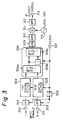
- Fig. 1 is a block diagram illustrating a typical constitution of a conventional digitized quadrature modulator. This modulator is constituted by replacing analog processing elements of an analog quadrature modulator with digital processing elements, respectively.
- reference numeral 100 denotes an in-phase channel (I-channel) signal input terminal, 101 a quadrature channel (Q-channel) signal input terminal, 102 an I-channel digital filter, 103 a Q-channel digital filter, 104 and 105 digital multipliers, 106 a digital adder, 107 a clock input terminal, 108 a counter, 109 a waveform generation ROM for producing carrier signals, 110 a digital-to-analog (D/A) converter, 111 a band pass filter (BPF), 112 a mixer, 113 a BPF, 114 an IF modulated signal output terminal and 115 a local oscillator, respectively.
- D/A digital-to-analog
- quadrature carrier signals are produced by the counter 108 and the ROM 109.
- the digital filters 102 and 103 receive input digital signals on n-sequence(s) (n is an integer equal to or greater than one) of I-channel and of Q-channel, respectively, to execute spectrum shaping and band limitation of these received signals.
- Baseband quadrature modulated output signal is provided by multiplying outputs from these digital filter 102 and 103 with the quadrature carrier signals at the multipliers 104 and 105, respectively, by adding outputs of the multipliers 104 and 105 at the adder 106, and thereafter by converting an output of the adder 106 into an analog signal at the D/A converter 110.
- Fig. 4a shows a timing chart of these signals in the conventional quadrature modulator.
- reference numeral 200 denotes an in-phase channel (I-channel) signal input terminal, 201 a quadrature channel (Q-channel) signal input terminal, 202 and 203 flip-flops for sampling input signals of respective channels, and 205 a digital filter.
- the digital filter 205 is constituted by a digital filtering portion for 0 phase 2050, a digital filtering portion for ⁇ /2 phase 2051, a digital filtering portion for ⁇ phase 2052 and a digital filtering portion for 3 ⁇ /2 phase 2053.
- reference numeral 206 denotes a four input multiplexer (4-to-1 selector), 207 a clock input terminal, 208 a 1/4 frequency divider, 209 a digital-to-analog (D/A) converter, 210 a band pass filter (BPF), 211 a mixer, 212 a BPF, 213 an IF modulated signal output terminal and 214 a local oscillator, respectively.
- This conventional modulator realizes quadrature modulation by using a fact that the amplitudes of each of quadrature carrier signals sampled at 0 phase, ⁇ /2 phase, ⁇ phase and 3 ⁇ /2 phase become as follows.
- the filtering portions 2050 to 2053 divided into the respective phases conduct the above calculation with the input signals of each channel, and the multiplexer 206 sequentially selects the calculated outputs from the filtering portions.
- reference numeral 300 denotes an in-phase channel (I-channel) signal input terminal, 301 a quadrature channel (Q-channel) signal input terminal, 302 and 303 flip-flops for sampling input signals of respective channels, 304 an I-channel digital filter, 305 a Q-channel digital filter and 306 a quadrature modulation circuit.
- the modulation circuit 306 is constituted by a two input multiplexer (2-to-1 selector) 306a, a bit inverter 306b and a two input multiplexer (2-to-1 selector) 306c.
- reference numeral 307 denotes a clock input terminal, 308 a 1/4 frequency divider, 309 a digital-to-analog (D/A) converter, 310 a band pass filter (BPF), 311 a mixer, 312 a BPF, 313 an IF modulated signal output terminal and 314 a local oscillator, respectively.
- D/A digital-to-analog
- BPF band pass filter
- This conventional modulator realizes quadrature modulation by using also the fact that the amplitudes of each of quadrature carrier signals sampled at 0 phase, ⁇ /2 phase, ⁇ phase and 3 ⁇ /2 phase become 1, 0, -1, 0 and 0, 1, 0, -1 as described above. Namely, outputs from the I-channel and Q-channel digital filters 304 and 305 are sequentially multiplexed by the multiplexer 306a, and then non-inverting and inverting paths of the multiplexed output are switched by means of the bit inverter 306b and the multiplexer 306c.
- a DSP quadrature modulator cannot directly produce modulated output signal at a radio frequency. Therefore, the baseband quadrature modulated output signal is first D/A converted and then the analog modulated output signal is up-converted into a desired frequency (IF or RF).
- IF or RF desired frequency
- DSP noises folding noises
- harmonic spurious components which may be produced during the frequency conversion
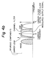
- Fig. 4b illustrates frequency arrangement of an output from the D/A converter in the conventional digitized quadrature modulator.
- a folding noise caused by the DSP DSP noise
- spurious components such as carrier leak and image caused by the frequency conversion appear near the IF modulated output signal.
- the design of the analog filter which must eliminate only these unnecessary spurious components without deteriorating transmission characteristics of the modulator becomes very difficult.
- a digitized quadrature modulator for receiving n-sequence(s) (n is an integer equal to or greater than one) of I-channel input digital signal and n-sequence(s) of Q-channel input digital signal, and for quadrature modulating the I-channel and Q-channel input digital signals by DSP, comprising: a digital filter for shaping the spectrum of the I-channel and Q-channel input digital signals to provide I-channel and Q-channel output signals, the output signals having a predetermined phase shift between the I-channel and the Q-channel so as to compensate a phase difference based upon the quadrature modulation by the DSP, complementary circuits for taking the complement of the I-channel and Q-channel output signals to provide I-channel and Q-channel complement signals, and a multiplexer circuit for multiplexing the I-channel and Q-channel output signals from the digital filter and the I-channel and Q-channel complement signals from the complementary circuits to provide a quadrature modulated output signal.
- the present invention provides a digitized quadrature modulator which can solve the above-mentioned problem of the conventional architecture, namely to provide a digitized quadrature modulator whereby its analog signal processing circuit can be easily designed.
- the present invention provides a digitized quadrature modulator which can variably control its modulation scheme and its transmission bandwidth.
- the present invention provides a digitized quadrature modulator whereby its circuit structure can be simplified without requesting an additional complicated control for its digital filter.
- the present invention provides a digitized quadrature modulator whereby, in response to different baud rates of input signals, modulated output signals can be produced without varying specifications of its analog signal processing circuit.
- the digital filter of the present invention is designed to provide a phase shift of (P I - P Q ) between the both channels, which corresponds to the timing phase difference of P dif between the both channels due to the DSP quadrature modulation, several cycles of carrier signals can be multiplied with an output of the digital filter without deteriorating transmission characteristics caused by the above-mentioned phase difference between the channels. Accordingly, the carrier frequency (the center frequency of the modulated output signal) can be optionally selected to a desired value without considering the operation conditions of the digital filter.
- the modulating part is constituted by the high-speed circuit such as the complementary circuits and the multiplexer circuit, it is very easy to raise the carrier frequency. If the carrier frequency is raised, folding noises (DSP noises) caused by the DSP and spurious components such as carrier leak and image caused by the frequency conversion will be produced at frequencies far from that of the modulated output signal. As a result, these DSP noise and spurious components can be sufficiently eliminated by an analog BPF having a relative wide bandpass width so as to not deteriorate transmission characteristics of the modulator. This causes the design of the analog signal processing circuit to become very easy.
- DSP noises folding noises
- spurious components such as carrier leak and image caused by the frequency conversion
- the digital filter includes an address generation circuit for multiplexing the input digital signals to generate an address signal, an waveform memory for storing waveform data having a predetermined phase shift between the I-channel and the Q-channel so as to compensate the phase difference caused by the quadrature modulation, and for outputting respective waveform data corresponding to a plurality of phases in response to the address signal, a plurality of weighting accumulators for weighting the respective waveform data from the memory to provide weighted data, and an adder for adding the weighted data.
- the complementary circuits consist of a first complementer for taking the complement of the I-channel output signal to provide an I-channel complement signal and a second complementer for taking the complement of the Q-channel output signal to provide a Q-channel complement signal
- the multiplexer circuit consists of a selector for sequentially multiplexing the I-channel output signal, the Q-channel output signal, the I-channel complement signal, and the Q-channel complement signal in this order to provide a quadrature modulated output signal.
- the digital filter may be constituted so that a phase of only the I-channel input digital signal or the Q-channel input digital signal is shifted by an amount of the phase difference based upon the quadrature modulation, or so that phases of the I-channel and Q-channel input digital signals are equally shifted toward the opposite direction with each other by a half amount of the phase difference based upon the quadrature modulation.
- the digital filter may be also constituted so that phases of the I-channel and Q-channel input digital signals are equally shifted toward the opposite direction with each other by a half amount of the phase difference based upon the quadrature modulation, and that the same filtering circuit is utilized from the both directions by inverting time base of the input digital signals.
- the filter circuit can be utilized in a time sharing manner without using a complicated additional circuit causing the circuit structure to simplify.
- the frequency of clock used in the digital filter will not be higher than that of the modulation clock even if the filter circuit is commonly used by the time sharing manner because the original clock frequency in the digital filter is less than a half of the modulation clock frequency.
- the digital filter includes an waveform memory for storing amplitude information having a predetermined phase shift between the I-channel and the Q-channel so as to compensate the phase difference based upon the quadrature modulation.
- the digital filter is constituted so that the number of samples per symbol M S in the digital filter is varied depending upon a baud rate control signal applied thereto.
- the digital filter may include an waveform memory having a plurality of ROMs for storing respective waveform data corresponding to a plurality of phases and the ROMs of a number which corresponds to the number of samples per symbol M S may be enabled to operate.
- the digital filter may include a plurality of weighting accumulators for weighting the respective waveform data from the ROMs to provide weighted data, and an adder for selecting the weighted data of a number which corresponds to the number of samples per symbol M S and for shift-adding the selected weighted data.
- variable baud rate control namely variable transmission bandwidth control is realized by forming a selection function without changing the operation condition of the digital filter. Therefore, if an analog BPF is designed to fit with the maximum baud rate mode, all the baud rate modes can be covered without changing specifications in the analog signal processing circuit.
- the conventional art never take account of adjusting the number of samples per symbol to variably control the baud rate. Namely, according to the conventional art, a new mode is started as soon as a switching signal for changing the baud rate is applied. Therefore, a phase discontinuity will occur at the mode switching point causing unnecessary noises to be produced. Thus, according to the conventional art, the digital filter has to be reset at the mode switching point.
- the mode switching can be completed in an instant.
- the I-channel and Q-channel input digital signals have a plurality of baud rates
- the modulator is constituted so that the number of samples per symbol M S is varied depending upon the baud rates to provide modulated output signals having the same center frequency with each other.
- modulated output signals can be obtained without changing circuit constant of the analog signal processing circuit, even when input signals have a plurality of baud rates.
- a plurality of DSP quadrature modulated output signals having the same center frequency can be produced by applying a control signal for indicating baud rate of the input signal to vary the sampling cycle in the digital filter.
- a BPF for eliminating DSP noises should be designed so as to eliminate the DSP noises without deteriorating transmission characteristics, with respect to the maximum baud rate input signal among various baud rate input signals. If so designed, since the number of samples per symbol with respect to the other input signals having lower baud rate is greater than that of the maximum rate signal, the DSP noises will be appeared out of the pass band of this BPF. Accordingly, such noises due to the various baud rate input signals can be effectively eliminated by a single BPF.
- the number of samples per symbol in the digital filter is varied in accordance with input signals having a plurality of baud rates and a BPF for eliminating DSP noises is designed to fit with the maximum baud rate input signal. Therefore, modulated output signals having the same center frequency can be obtained resulting no need for changing circuit constant of the analog signal processing circuit, even when input signals have a plurality of baud rates.
- the digital filter includes a circuit for selectively clearing the waveform data from the ROMs in response to a modulation scheme control signal applied thereto.
- variable modulation scheme control can be realized by the clearing function with respect to the outputs from the waveform memory without changing the operation condition of the digital filter. Therefore, not only the mode switching of the modulation scheme can be completed in a moment, but also an advanced facility can be easily added without changing specifications in the analog signal processing circuit.
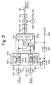
- Fig. 5 is a block diagram which schematically shows a whole constitution of a preferred embodiment of a digitized quadrature modulator according to the present invention.
- reference numeral 500 denotes an in-phase channel (I-channel) signal input terminal, 501 a quadrature channel (Q-channel) signal input terminal, 502 a flip-flop connected to the signal input terminal 500 for sampling I-channel input signal, 503 a flip-flop connected to the signal input terminal 501 for sampling Q-channel input signal, and 504 a digital filter.
- I-channel in-phase channel
- Q-channel quadrature channel
- 502 a flip-flop connected to the signal input terminal 500 for sampling I-channel input signal
- 503 a flip-flop connected to the signal input terminal 501 for sampling Q-channel input signal
- 504 a digital filter.
- the digital filter 504 is constituted, in this embodiment, by an I-channel digital filter portion 504a, a Q-channel digital filter portion 504b, a circuit 504c for providing an impulse response r(t + P I ) with phase shift amount of P I to the I-channel digital filter portion 504a, and a circuit 504d for providing an impulse response r(t + P Q ) with phase shift amount of P Q to the Q-channel digital filter portion 504b, where r(t) corresponds a normal impulse response of each the digital filter portions 504a and 504b.
- An output terminal of the I-channel filter portion 504a is connected directly to a first input terminal of a four input multiplexer (4-to-1 selector) 505c in a quadrature modulation circuit 505, and also connected to a third input terminal of the multiplexer 505c via a first complementer 505a for taking the complement of its input signal.
- An output terminal of the Q-channel filter portion 504b is connected directly to a second input terminal of the multiplexer 505c, and also connected to a fourth input terminal of the multiplexer 505c via a second complementer 505b for taking the complement of its input signal.
- a clock input terminal 506 is connected to a 1/4 clock frequency divider 507 and to a clock input terminal of the multiplexer 505c.
- An output terminal of the divider 507 is connected to clock input terminals of the digital filter portions 504a and 504b, and also to control terminals of the flip-flops 502 and 503 via a 1/4 clock frequency divider 508.
- An output terminal of the multiplexer 505c is coupled to an IF modulated signal output terminal 513 via a digital-analog (D/A) converter 509, a bandpass filter (BPF) 510, a mixer 511 and a BPF 512. To the mixer 511, an output terminal of a local oscillator 514 is also connected.
- D/A digital-analog
- BPF bandpass filter
- I-channel and Q-channel input signals are sampled by clocks having 1/16 frequency of the system clock (clock for the modulation), and then the sampled signals are applied to the I-channel and Q-channel filter portions 504a and 504b, respectively. These signals are outputted after being spectrum-shaped and bandlimited in the filter portions to the quadrature modulation circuit 505.
- the I-channel and Q-channel outputs from the filter 504 and inverted signals of these outputs are multiplexed at a predetermined sequence (i.e. first, output (I) from the I-channel filter 504a, then, output (Q) from the Q-channel filter 504b, then, output ( I ⁇ ) from the first complementer 505a, and lastly, output ( Q ⁇ ) from the second complementer 505b) at every time slot of the output, by means of the multiplexer 505c, and thus, baseband quadrature modulated output signal as shown in Fig. 6a is provided.
- a predetermined sequence i.e. first, output (I) from the I-channel filter 504a, then, output (Q) from the Q-channel filter 504b, then, output ( I ⁇ ) from the first complementer 505a, and lastly, output ( Q ⁇ ) from the second complementer 505b
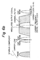
- the modulation circuit 505 is constituted by the high-speed circuit such as the complementers and the selector, it is very easy to raise the carrier frequency (center frequency of an IF modulated output signal). If the carrier frequency is raised, as shown in Fig. 6b, folding noises (DSP noises) caused by the DSP and spurious components such as carrier leak and image caused by the frequency conversion will be produced at frequencies far from that of the IF modulated output signal (carrier frequency). As a result, these DSP noise and spurious components can be sufficiently eliminated by an analog BPF having a relative wide bandpass width so as to not deteriorate transmission characteristics of the modulator. This causes the design of the analog signal processing components to become very easy.
- DSP noises folding noises
- spurious components such as carrier leak and image caused by the frequency conversion
- phase of the digital filter 504 is preliminarily shifted between the I-channel and the Q-channel by an appropriate amount so as to compensate the phase difference caused by the data multiplexing.
- the digital filter 504 has different tap coefficients and thus provides a phase shift of an amount of P I - P Q between the both channels.
- This phase shift amount is produced by the circuit 504c which provides an impulse response r(t + P I ) to the I-channel digital filter portion 504a, and by the circuit 504d which provides an impulse response r(t + P Q ) to the Q-channel digital filter portion 504b, where r(t) is a single impulse response of each the digital filter portions 504a and 504b.
- phase difference P dif T / (M s ⁇ 2M C ) where T is a symbol period (therefore 1/T is a symbol rate), M S is the number of samples per symbol in the digital filter and M C / 2 is a carrier cycle per an output data from the filter.
- T a symbol period (therefore 1/T is a symbol rate)
- M S the number of samples per symbol in the digital filter
- M C / 2 is a carrier cycle per an output data from the filter.
- phase shift can be indicated by using impulse response of each channel as follows.
- Fig. 9 is a block diagram of a concrete constitution of each of the digital filter portions 504a and 504b shown in Fig. 5.
- reference numeral 900 denotes a signal input terminal
- 9010 to 901 (K-1) denote delay circuits each having a delay period of T (symbol period), connected to the input terminal 900 in series.
- Output terminals of the respective delay circuits 9011 to 901 (K-1) are connected to input terminals of an waveform memory 902.
- the waveform memory 902 is constituted in this example by four ROMs 9020 to 9023 which preliminarily store amplitude information with respect to respective phases (Phase-0 to Phase-3). These information can be read out in response to an address which will be formed by outputs from the delay circuits.
- the amplitude information stored in the ROMS 9020 to 9023 are phase-shifted by P I in the I-channel to provide the impulse response r(t + P I ) and also phase-shifted by P Q in the Q-channel to provide the impulse response r(t + P Q ), so that the phase shift amount between the both channels becomes equal to P I - P Q .
- Output terminals of the ROMS 9020 to 9023 are connected to input terminals of a full adder 904 directly, via a T/4 delay circuit 9031, via two T/4 delay circuits 9032 and 9033, and via three T/4 delay circuits 9034 to 9036, respectively.
- An output terminal 905 of the full adder 904 is connected to the one channel input terminal of the quadrature modulation circuit 505 in Fig. 5.
- the digital filter of this example provides the phase shift P I - P Q between the both channels by preliminarily phase-shifting the amplitude information stored in the memory 902.
- Fig. 10 shows an another constitution of the digital filter which can provide the phase shift P I - P Q between the both channels.
- This digital filter is constituted by a single spectrum shaping filter of FIR type instead of the two digital filter portions 504a and 504b of the respective channels, shown in Fig. 5.
- the tap coefficient for the I-channel is used as the tap coefficient for the Q-channel by inverting its time base and vice versa so that the tap coefficients are shared in both channels.
- reference numeral 1000 denotes an I-channel signal input terminal, 1001 a Q-channel signal input terminal, 10020 to 1002 (K-1) delay circuits each having a delay period of ⁇ , connected to the I-channel input terminal 1000 in series, and 10030 to 1003 (K-1) delay circuits each having a delay period of ⁇ , connected to the Q-channel input terminal 1001 in series.
- the I-channel input terminal 1000 and an output terminal of the delay circuit 1003 (K-1) are connected to an input terminals of a two input multiplexer (2-to-1 selector) 10040, output terminals of the delay circuits 10020 and 1003 (K-2) are connected to an input terminals of a two input multiplexer 10041,...., output terminals of the delay circuits 1002 (K-2) and 10031 are connected to an input terminals of a two input multiplexer 1004 (K-1) , and an output terminal of the delay circuit 1002 (K-1) and the Q-channel input terminal 1001 are connected to an input terminals of a two input multiplexer 1004 K , respectively.
- Output terminals of the 2-to-1 selectors 10040 to 1004 K are connected to one input terminals of multipliers 10050 to 1005 K , respectively. To the other input terminals of the multipliers 10050 to 1005 K , tap coefficients a0 to a K are applied, respectively. Output terminals of the multipliers 10050 to 1005 K are connected to input terminals of demultiplexers (1-to-2 dividers) 10060 to 1006 K . Two output terminals of each the 1-to-2 dividers 10060 to 1006 K are connected to input terminals of multi-input adders 1007 and 1008, respectively. Output terminals of the multi-input adders 1007 and 1008 are connected to an I-channel output terminal 1009 and a Q-channel output terminal 1010, respectively.
- Outputs from the multipliers 10050 to 1005 K are demultiplexed by the 1-to-2 dividers 10060 to 1006 K into the respective channels, and then all the tap outputs from the 1-to-2 dividers are added with each other at the multi-input adders 1007 and 1008 to provide respective channel outputs of the digital filter.
- Fig. 11 shows a still another constitution of the digital filter which can also provide the phase shift P I - P Q between the both channels.
- This digital filter is constituted by a single spectrum shaping filter of BTF type instead of the two digital filter portions 504a and 504b of the respective channels, shown in Fig. 5.
- reference numeral 1100 denotes an I-channel signal input terminal, 1101 a Q-channel signal input terminal, 11020 to 1102 (K-1) delay circuits each having a delay period of T, connected to the I-channel input terminal 1100 in series, and 11030 to 1103 (K-1) delay circuits each having a delay period of T, connected to the Q-channel input terminal 1101 in series.
- the I-channel input terminal 1100 and an output terminal of the delay circuit 1103 (K-1) , output terminals of the delay circuits 11020 and 1103 (K-2) ,...., output terminals of the delay circuits 1102 (K-2) and 11031, and an output terminal of the delay circuit 1102 (K-1) and the Q-channel input terminal 1101 are connected to input terminals of the 2-to-1 selectors 11040 to 1104 K , respectively.
- Output terminals of the 2-to-1 selectors 11040 to 1104 K are connected to one input terminals of waveform ROMs 11050 to 1105 K which preliminarily store amplitude information with respect to respective phases (Phase-0 to Phase-3), respectively.
- Output terminals of the waveform ROMs 11050 to 1105 K are connected to input terminals of demultiplexers (1-to-2 dividers) 11060 to 1106 K .
- One output terminal of the 1-to-2 dividers 11060 is directly connected to an input terminal of a multi-input adder 1108, and the other input terminal is connected to an input terminal of a multi-input adder 1109 via a 3T/4 delay circuit 11071.
- One output terminal of the 1-to-2 dividers 11061 is connected to an input terminal of the multi-input adder 1108 via a T/4 delay circuit 11072, and the other input terminal is connected to an input terminal of the multi-input adder 1109 via a T/2 delay circuit 11073.
- One output terminal of the 1-to-2 dividers 11062 is connected to an input terminal of the multi-input adder 1108 via a T/2 delay circuit 11074, and the other input terminal is connected to an input terminal of the multi-input adder 1109 via a T/4 delay circuit 11075.
- One output terminal of the 1-to-2 dividers 11063 is connected to an input terminal of the multi-input adder 1108 via a 3T/4 delay circuit 11076, and the other input terminal is directly connected to an input terminal of the multi-input adder 1109.
- Output terminals of the multi-input adders 1108 and 1109 are connected to an I-channel output terminal 1110 and a Q-channel output terminal 1111, respectively.
- Input signals of the both channels are shifted by a period of T to the opposite directions with each other by means of the delay circuits 11020 to 1102 (K-1) and 11030 to 1103 (K-1) , and then multiplexed by the 2-to-1 selectors 11040 to 1104 K . These information can be read out in response to an address which will be formed by the outputs from the delay circuits. Thereafter, the multiplexed outputs from the 2-to-1 selectors are applied to the waveform ROMs 11050 to 11053 of respective phases as addresses, and thus amplitude information are read out from the waveform ROMs.
- Outputs from the ROMs 11050 to 11053 are demultiplexed by the 1-to-2 dividers 11060 to 11063 into the respective channels, and then output signals of Phase-0 to Phase-3 in the each channel are respectively delayed as follows. Thereafter, all the tap outputs are added with each other at the multi-input adders 1108 and 1109 to provide respective channel outputs of the digital filter.
- the signal phases in the I-channel and Q-channel are equally shifted toward advance and delay directions by a half (P dif / 2) of the phase difference P dif produced between the I-channel and the Q-channel due to the DSP quadrature modulation, and also the same filter circuit is utilized from the both directions to invert its time base, so that a phase shift corresponding to the phase difference Pdif is provided between the input signals of the I-channel and the Q-channel.
- the phase characteristics of the digital filter is designed to be shifted toward advance and delay directions by P dif / 2 and the tap coefficients for the both channels are used by inverting their time base.
- the filter circuit can be utilized in a time sharing manner without using a complicated additional circuit causing the circuit structure to simplify.
- the frequency of clock used in the digital filter will not be higher than that of the modulation clock even if the filter circuit is commonly used by the time sharing manner because the original clock frequency in the digital filter is less than a half of the modulation clock frequency.
- Fig. 12 is a block diagram which schematically shows a whole constitution of an another embodiment of a digitized quadrature modulator according to the present invention.
- the quadrature modulator of this embodiment has a variable baud rate control function in addition to the functions provided in the modulator of Fig. 5.
- reference numeral 1200 denotes an in-phase channel (I-channel) signal input terminal, 1201 a quadrature channel (Q-channel) signal input terminal, 1202 a flip-flop connected to the signal input terminal 1200 for sampling I-channel input signal, 1203 a flip-flop connected to the signal input terminal 1201 for sampling Q-channel input signal, and 1204 a digital filter.
- I-channel in-phase channel
- Q-channel quadrature channel
- 1202 a flip-flop connected to the signal input terminal 1200 for sampling I-channel input signal
- 1203 a flip-flop connected to the signal input terminal 1201 for sampling Q-channel input signal
- 1204 a digital filter.
- the digital filter 1204 is constituted, in this embodiment, by an I-channel digital filter portion 1204a, a Q-channel digital filter portion 1204b, a circuit 1204c for providing an impulse response r(t + P I ) with phase shift amount of P I to the I-channel filter portion 1204a, and a circuit 1204d for providing an impulse response r(t + P Q ) with phase shift amount of P Q to the Q-channel filter portion 1204b, where r(t) corresponds a normal impulse response of each the digital filter portions 1204a and 1204b.
- An output terminal of the I-channel filter portion 1204a is connected directly to a first input terminal of a four input multiplexer (4-to-1 selector) 1205c in a quadrature modulation circuit 1205, and also connected to a third input terminal of the multiplexer 1205c via a first complementer 1205a for taking the complement of its input signal.
- An output terminal of the Q-channel filter portion 1204b is connected directly to a second input terminal of the multiplexer 1205c, and also connected to a fourth input terminal of the multiplexer 1205c via a second complementer 1205b for taking the complement of its input signal.
- a clock input terminal 1206 is connected to a 1/4 clock frequency divider 1207 and to a clock input terminal of the multiplexer 1205c.
- An output terminal of the divider 1207 is connected to clock input terminals of the digital filter portions 1204a and 1204b, and also to control terminals of the flip-flops 1202 and 1203 via a 1 / M S clock frequency divider 1208.
- An output terminal of the multiplexer 1205c is coupled to an IF modulated signal output terminal 1213 via a digital-analog (D/A) converter 1209, a bandpass filter (BPF) 1210, a mixer 1211 and a BPF 1212. To the mixer 1211, an output terminal of a local oscillator 1214 is also connected.
- D/A digital-analog
- BPF bandpass filter
- An input terminal 1215 which will receive a baud rate control signal is connected to control inputs of the 1 / M S clock frequency divider 1208 and of the digital filter 1204.
- I-channel and Q-channel input signals are sampled by clocks having 1 / 4M S frequency of the system clock (clock for the modulation), and then the sampled signals are applied to the I-channel and Q-channel filter portions 1204a and 1204b, respectively. These signals are outputted after being spectrum-shaped and bandlimited in the digital filter portions to the quadrature modulation circuit 1205.
- the I-channel and Q-channel outputs from the filter 1204 and inverted signals of these outputs are multiplexed at a predetermined sequence (i.e. first, output (I) from the I-channel filter 1204a, then, output (Q) from the Q-channel filter 1204b, then, output ( I ⁇ ) from the first complementer 1205a, and lastly, output ( Q ⁇ ) from the second complementer 1205b) at every time slot of the output, by means of the multiplexer 1205c, and thus, baseband quadrature modulated output signal is provided.
- a predetermined sequence i.e. first, output (I) from the I-channel filter 1204a, then, output (Q) from the Q-channel filter 1204b, then, output ( I ⁇ ) from the first complementer 1205a, and lastly, output ( Q ⁇ ) from the second complementer 1205b
- the modulation circuit 1205 is constituted by the high-speed circuit such as the complementers and the selector, it is very easy to raise the carrier frequency (center frequency of an IF modulated output signal). If the carrier frequency is raised, as shown in Fig. 6b, folding noises (DSP noises) caused by the DSP and spurious components such as carrier leak and image caused by the frequency conversion will be produced at frequencies far from that of the IF modulated output signal (carrier frequency). As a result, these DSP noise and spurious components can be sufficiently eliminated by an analog BPF having a relative wide bandpass width so as to not deteriorate transmission characteristics of the modulator. This causes the design of the analog signal processing components to become very easy.
- DSP noises folding noises
- spurious components such as carrier leak and image caused by the frequency conversion
- phase of the digital filter 1204 is preliminarily shifted between the I-channel and the Q-channel by an appropriate amount so as to compensate the phase difference caused by the data multiplexing.
- the digital filter 1204 has different tap coefficients and thus provides a phase shift of an amount of P I - P Q between the both channels.
- This phase shift amount is produced by the circuit 1204c which provides an impulse response r(t + P I ) to the I-channel digital filter portion 1204a, and by the circuit 1204d which provides an impulse response r(t + P Q ) to the Q-channel digital filter portion 1204b, where r(t) is a single impulse response of each the digital filter portions 1204a and 1204b.
- the operation speed in the digital filter 1204 and in the quadrature modulation circuit 1205 is constant (clock cycle is T/4).
- the number of selectable baud rate is not limited to two as aforementioned, but can be determined to any value more than two.
- modulated output signals can be obtained without changing circuit constant of the analog signal processing circuit, even when input signals have a plurality of baud rates.
- a plurality of DSP quadrature modulated output signals having the same center frequency can be produced by applying a control signal for indicating baud rate of the input signal to vary the sampling cycle in the digital filter.
- the BPF for eliminating DSP noises should be designed so as to eliminate the DSP noises without deteriorating transmission characteristics, with respect to the maximum baud rate input signal among various baud rate input signals. If so designed, since the number of samples per symbol with respect to the other input signals having lower baud rate is greater than that of the maximum rate signal, the DSP noises will be appeared out of the pass band of this BPF. Accordingly, such noises due to the various baud rate input signals can be effectively eliminated by a single BPF.
- the number of samples per symbol in the digital filter is varied in accordance with input signals having a plurality of baud rates and a BPF for eliminating DSP noises is designed to fit with the maximum baud rate input signal. Therefore, modulated output signals having the same center frequency can be obtained resulting no need for changing circuit constant of the analog signal processing circuit, even when input signals have a plurality of baud rates.
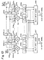
- Fig. 13 is a block diagram which schematically shows a whole constitution of a still another embodiment of a digitized quadrature modulator according to the present invention.
- reference numeral 1300 denotes an in-phase channel (I-channel) input terminal for four input signals (D1 to D4), 1301 a quadrature channel (Q-channel) input terminal for four input signals (D1 to D4), 1302 flip-flops connected to the signal input terminal 1300 for sampling I-channel input signals, 1303 flip-flops connected to the signal input terminal 1301 for sampling Q-channel input signals, and 1304 a digital filter.
- I-channel in-phase channel
- D1 to D4 quadrature channel
- Q-channel quadrature channel
- 1302 flip-flops connected to the signal input terminal 1300 for sampling I-channel input signals
- 1303 flip-flops connected to the signal input terminal 1301 for sampling Q-channel input signals
- 1304 a digital filter.
- the digital filter 1304 is constituted, in this embodiment, by an I-channel digital filter portion 1304a, a Q-channel digital filter portion 1304b, a circuit 1304c for providing an impulse response r(t + P I ) with phase shift amount of P I to the I-channel filter portion 1304a, and a circuit 1304d for providing an impulse response r(t + P Q ) with phase shift amount of P Q to the Q-channel filter portion 1304b, where r(t) corresponds a normal impulse response of each the digital filter portions 1304a and 1304b.
- An output terminal of the I-channel digital filter portion 1304a is connected directly to a first input terminal of a four input multiplexer (4-to-1 selector) 1305c in a quadrature modulation circuit 1305, and also connected to a third input terminal of the multiplexer 1305c via a first complementer 1305a for taking the complement of its input signal.
- An output terminal of the Q-channel digital filter portion 1304b is connected directly to a second input terminal of the multiplexer 1305c, and also connected to a fourth input terminal of the multiplexer 1305c via a second complementer 1305b for taking the complement of its input signal.
- a clock input terminal 1306 is connected to a 1/4 clock frequency divider 1307 and to a clock input terminal of the multiplexer 1305c.
- An output terminal of the divider 1307 is connected to clock input terminals of the digital filter portions 1304a and 1304b, and also to control terminals of the flip-flops 1302 and 1303 via a 1 / M S clock frequency divider 1308.
- An output terminal of the multiplexer 1305c is coupled to an IF modulated signal output terminal 1313 via a digital-analog (D/A) converter 1309, a bandpass filter (BPF) 1310, a mixer 1311 and a BPF 1312. To the mixer 1311, an output terminal of a local oscillator 1314 is also connected.
- D/A digital-analog
- BPF bandpass filter
- An input terminal 1315 which will receive a baud rate control signal is connected to control inputs of the 1 / M S clock frequency divider 1308 and of the digital filter 1304.
- An input terminal 1316 which will receive a modulation scheme control signal is connected to the digital filter 1304.
- I-channel and Q-channel input signals are sampled by clocks having 1 / 4M S frequency of the system clock (clock for the modulation), and then the sampled signals are applied to the I-channel and Q-channel filter portions 1304a and 1304b, respectively. These signals are outputted after being spectrum-shaped and bandlimited in the filter portions to the modulation circuit 1305.
- I-channel and Q-channel outputs from the filter 1304 and inverted signals of these outputs are multiplexed at a predetermined sequence (i.e. first, output (I) from the I-channel filter 1304a, then, output (Q) from the Q-channel filter 1304b, then, output ( I ⁇ ) from the first complementer 1305a, and lastly, output ( Q ⁇ ) from the second complementer 1305b) at every time slot of the output, by means of the multiplexer 1305c, and thus, baseband quadrature modulated output signal is provided.
- a predetermined sequence i.e. first, output (I) from the I-channel filter 1304a, then, output (Q) from the Q-channel filter 1304b, then, output ( I ⁇ ) from the first complementer 1305a, and lastly, output ( Q ⁇ ) from the second complementer 1305b
- the modulation circuit 1305 is constituted by the high-speed circuit such as the complementers and the selector, it is very easy to raise the carrier frequency (center frequency of an IF modulated output signal). If the carrier frequency is raised, as shown in Fig. 6b, folding noises (DSP noises) caused by the DSP and spurious components such as carrier leak and image caused by the frequency conversion will be produced at frequencies far from that of the IF modulated output signal (carrier frequency). As a result, these DSP noise and spurious components can be sufficiently eliminated by an analog BPF having a relative wide bandpass width so as to not deteriorate transmission characteristics of the modulator. This causes the design of the analog signal processing components to become very easy.
- DSP noises folding noises
- spurious components such as carrier leak and image caused by the frequency conversion
- phase of the digital filter 1304 is preliminarily shifted between the I-channel and the Q-channel by an appropriate amount so as to compensate the phase difference caused by the data multiplexing.
- the digital filter 1304 has different tap coefficients and thus provides a phase shift of an amount of P I - P Q between the both channels.
- This phase shift amount is produced by the circuit 1304c which provides an impulse response r(t + P I ) to the I-channel filter portion 1304a, and by the circuit 1304d which provides an impulse response r(t + P Q ) to the Q-channel filter portion 1304b, where r(t) is a single impulse response of each the digital filter portions 1304a and 1304b.
- the operation speed in the digital filter 1304 and in the modulation circuit 1305 is constant (clock cycle is T/4).
- the number of selectable baud rate is not limited to two as aforementioned, but can be determined to any value more than two.
- the modulation scheme can be variably selected from multivalued modulation of QPSK to 256QAM.
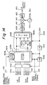
- Fig. 14 is a block diagram which schematically shows a whole constitution of a further embodiment of a digitized quadrature modulator according to the present invention.
- the modulator of this embodiment receives n-sequences (n-4) input signals and has a variable baud rate control function and a variable modulation scheme control function in addition to the functions provided in the modulator of Fig. 5.
- reference numeral 1400 denotes an in-phase channel (I-channel) input terminal for four input signals (D1 to D4), 1401 a quadrature channel (Q-channel) input terminal for four input signals (D1 to D4), 1402 flip-flops connected to the signal input terminal 1400 for sampling I-channel input signals and to the signal input terminal 1401 for sampling Q-channel input signals, and 1404 a digital filter.
- the digital filter 1404 is constituted, in this embodiment, by a digital filter portion 1404a commonly used for the I-channel and Q-channel, and a circuit 1404b for providing an impulse response r(t + P/2) with phase shift of P/2 to the filter portion 1404a, where r(t) corresponds a normal impulse response of the digital filter portion 1404a.
- An I-channel output terminal of the filter portion 1404a is connected directly to a first input terminal of a four input multiplexer (4-to-1 selector) 1405c in a quadrature modulation circuit 1405, and also connected to a third input terminal of the multiplexer 1405c via a first complementer 1405a for taking the complement of its input signal.
- a Q-channel output terminal of the filter portion 1404a is connected directly to a second input terminal of the multiplexer 1405c, and also connected to a fourth input terminal of the multiplexer 1405c via a second complementer 1405b for taking the complement of its input signal.
- a clock input terminal 1406 is connected to a 1/4 clock frequency divider 1407 and to a clock input terminal of the multiplexer 1405c.
- An output terminal of the divider 1407 is connected to a clock input terminal of the filter portion 1404a, and also to a control terminal of the flip-flops 1402 via a 1 / M S clock frequency divider 1408.
- An output terminal of the multiplexer 1405c is coupled to an IF modulated signal output terminal 1413 via a digital-analog (D/A) converter 1409, a bandpass filter (BPF) 1410, a mixer 1411 and a BPF 1412. To the mixer 1411, an output terminal of a local oscillator 1414 is also connected.
- D/A digital-analog
- BPF bandpass filter
- An input terminal 1415 which will receive a baud rate control signal is connected to control inputs of the 1 / M S clock frequency divider 1408 and of the digital filter 1404.
- An input terminal 1416 which will receive a modulation scheme control signal is connected to the digital filter 1404.
- I-channel and Q-channel input signals are sampled by clocks having 1 / 4M S frequency of the system clock (clock for the modulation), and then the sampled signals are applied to the filter portion 1404a. These signals are outputted after being spectrum-shaped and bandlimited in the filter portion to the modulation circuit 1405.
- the I-channel and Q-channel outputs from the filter 1404 and inverted signals of these outputs are multiplexed at a predetermined sequence (i.e. first, I-channel output (I) from the digital filter, then, Q-channel output (Q) the digital filter, then, output ( I ⁇ ) from the first complementer 1405a, and lastly, output ( Q ⁇ ) from the second complementer 1405b) at every time slot of the output, by means of the multiplexer 1405c, and thus, baseband quadrature modulated output signal is provided.
- a predetermined sequence i.e. first, I-channel output (I) from the digital filter, then, Q-channel output (Q) the digital filter, then, output ( I ⁇ ) from the first complementer 1405a, and lastly, output ( Q ⁇ ) from the second complementer 1405b
- the quadrature modulation circuit 1405 is constituted by the high-speed circuit such as the complementers and the selector, it is very easy to raise the carrier frequency (center frequency of an IF modulated output signal). If the carrier frequency is raised, as shown in Fig. 6b, folding noises (DSP noises) caused by the DSP and spurious components such as carrier leak and image caused by the frequency conversion will be produced at frequencies far from that of the IF modulated output signal (carrier frequency). As a result, these DSP noise and spurious components can be sufficiently eliminated by an analog BPF having a relative wide bandpass width so as to not deteriorate transmission characteristics of the modulator. This causes the design of the analog signal processing components to become very easy.
- DSP noises folding noises
- spurious components such as carrier leak and image caused by the frequency conversion
- phase of the digital filter 1404 is preliminarily shifted between the I-channel and the Q-channel by an appropriate amount so as to compensate the phase difference caused by the data multiplexing.
- This phase shift amount is produced by the circuit 1404b which provides an impulse response r(t + P I ) to the I-channel side and provides an impulse response r(t + P Q ) to the Q-channel side, where r(t) is a single impulse response of the filter portion 1404a.
- phase difference P dif T / (M s ⁇ 2M C ) where T is a symbol period, M S is the number of samples per symbol in the digital filter and M C / 2 is a carrier cycle per an output data from the filter.
- the phase difference P dif is equal to T / 4M S .
- the operation speed in the digital filter 1404 and in the modulation circuit 1405 is constant (clock cycle is T/4).
- the number of selectable baud rate is not limited to two as aforementioned, but can be determined to any value more than two.
- the modulation scheme can be variably selected from multivalued modulation of QPSK to 256QAM.
- Fig. 15 is a block diagram showing a concrete constitution of one channel part of the digital filter 1404 according to the embodiment of Fig. 14, of the I-channel digital filter portion 1304a according to the embodiment of Fig.13, or of the Q-channel digital filter portion 1304b according to the embodiment of Fig. 13.
- reference numeral 1501 denotes an address generation circuit for multiplexing input signals (D1, D2, D3, D4) applied thereto via four input terminals 1500.
- This circuit 1501 is constituted by four shift registers 1501a1 to 1501a4 for delaying the respective input signals and a four input multiplexer (4-to-1 selector) 1501b for multiplexing output signals from these shift registers.
- An output terminal of the circuit 1501 is connected to an address input terminal of an waveform memory 1502.
- a baud rate control signal will be applied via the input terminal 1415 (Fig. 14).
- Output terminals of this memory 1502 is connected to input terminals of a register and timing control circuit 1503, respectively.
- a modulation scheme control signal will be applied via the input terminal 1416 (Fig. 14).
- Output terminals of the circuit 1503 are connected to input terminals of weighting accumulators 15040 to 15047 for the respective phases Phase-0 to Phase-7, respectively. Output terminals of these accumulators 15040 to 15047 are connected to input terminals of a shift adder 1505. An output terminal of the shift adder 1505 is connected to the quadrature modulation circuit 1305 or 1405 in Fig. 13 or 14.
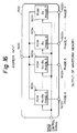
- Fig. 16 is a block diagram of a concrete constitution of the waveform memory 1502 shown in Fig. 15.
- the waveform memory 1502 is constituted by a plurality, for example eight in this case, of ROMs 16010 to 16017.
- the number of the ROMs is equal to the maximum tap number.
- These ROMs preliminarily store amplitude information with respect to respective phases (Phase-0 to Phase-7). These information can be read out in response to an address applied from the address generation circuit 1501 (Fig. 15) via an input terminal 1600.
- the read information will be outputted to the register and timing control circuit 1503 (Fig. 15) via output terminals 16020 to 16027.
- the amplitude information stored in the ROMS 16010 to 16017 are phase-shifted by P I in the I-channel to provide the impulse response r(t + P I ) and also phase-shifted by P Q in the Q-channel to provide the impulse response r(t + P Q ), so that the phase shift amount between the both channels becomes equal to P I - P Q .
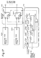
- Fig. 17 is a block diagram of a concrete constitution of the register and timing control circuit 1503 shown in Fig. 15.
- This circuit 1503 is constituted by a register portion 1700 and a timing control circuit 1701.
- the register portion 1700 has flip-flops 17000 to 17007 for the respective phases. To D-input terminals of these flip-flops, outputs from the ROMs 16010 to 16017 are applied, respectively. Q-output terminals of the flip-flops are connected to the input terminals of the weighting accumulators 15040 to 15047 shown in Fig. 15, respectively.
- Fig. 18 illustrates a timing chart of this timing control circuit 1701.
- the clock having the operation frequency f ROMCK is frequency-divided to f ROMCK / 8 by the divider 1701a, and delayed respectively by its original cycle (1 / f ROMCK ) at the delay circuits.
- These delayed clocks are applied to the 4-to-1 selector 1701c.
- the selection of one of four inputs in the selector 1701c is controlled by the modulation scheme control signal. For example, if "1 input” is selected as an input of the selector, the output from the timing control circuit 1701 will be "1 input” as indicated in Fig.
- Fig. 19 is a block diagram of a concrete constitution of each of the weighting accumulators 15040 to 15047 for the respective phases (Phase-0 to Phase-7) shown in Fig. 15.
- Each of the weighting accumulators is constituted by an adder 1900, a multiplier 1901 for doubling its input and for outputting the result to the adder 1900, a register 1902 with a clear signal input terminal (not shown) for feeding output from the adder 1900 back to the multiplier 1901, and a register 1903 for receiving the output from the adder 1900.
- Fig. 20 is a block diagram of a concrete constitution of the shift adder 1505 shown in Fig. 15.
- the shift adder is constituted by an 8-to-1 selector 2000 for sequentially selecting outputs from the weighting accumulators 15040 to 15047 to output the selected signals in series, 4-stage shift registers 2001 and 2002 for delaying each of sequential outputs from the selector 2000 by a sampling cycle, an 8-input adder 2003 for adding parallel inputs from the shift registers 2001 and 2002, and a counter 2004 for controlling a reset value of the selector 2000.
- the maximum count number of the counter is set so that the selector 2000 sequentially selects the accumulator outputs of Phase-0 to Phase-7.
- Input signals D1, D2, D3, D4 sampled by the clock having a cycle of M S times as long as that of the operation clock in the digital filter are delayed respectively by the shift registers 1501a1 to 1501a4 and then multiplexed by the multiplexer 1501b to produce a ROM address shown in Fig. 21.
- waveform responses preliminarily stored in the ROMs 16010 to 16017 (Fig. 16) in the waveform memory 1502 are read out.
- the amplitude information stored in the ROMS 16010 to 16017 are phase-shifted by P I in the I-channel and also phase-shifted by P Q in the Q-channel.
- the phase shift amount provided between the both channels will be equal to P I - P Q .
- Output data from the waveform memory 1502 with respect to the respective phases are applied to the register and timing control circuit 1503 and data in a slot or slots designated by the modulation scheme control signal are cleared to 0. For example, if “1 input” is selected depending upon the modulation scheme control signal, data in slots of D2, D3 and D4 are cleared to 0. If “2 input” is selected, data in slots of D3 and D4 are cleared to 0. If “3 input” is selected, data in a slot of D4 are cleared to 0. If “4 input” is selected, no data is cleared to 0.
- Outputs from the circuit 1503 are applied to the respective weighting accumulators 15040 to 15047 wherein an weighting accumulation of D1 + D2/2 + D3/4 + D4/8 is executed.
- amplitude information depending upon the selected one of modulation schemes QPSK to 256QAM can be provided.
- the reset value of the counter 2004 (Fig. 20) is switched in accordance with the number corresponding to the number of samples per symbol, which is designated by the baud rate control signal so as to select desired phase outputs from the weighting accumulators 15040 to 15047.
- the digital filter according to this embodiment is designed to provide a phase shift of an amount which corresponds to the phase difference of P dif between the both channels due to an absence of partial data on one channel.
- the carrier frequency (the center frequency of the modulated output signal) can be optionally selected to a desired value without considering the operation conditions of the digital filter.
- the modulation circuit is constituted by the high-speed circuit such as the complementers and the selector, it is very easy to raise the carrier frequency. If the carrier frequency is raised, folding noises (DSP noises) caused by the DSP and spurious components such as carrier leak and image caused by the frequency conversion will be produced at frequencies far from that of the modulated output signal. As a result, these DSP noise and spurious components can be sufficiently eliminated by an analog BPF having a relative wide bandpass width so as to not deteriorate transmission characteristics of the modulator. This causes the design of the analog signal processing circuit to become very easy.
- DSP noises folding noises
- spurious components such as carrier leak and image caused by the frequency conversion
- variable baud rate control namely variable transmission bandwidth control is realized by forming a selection function without changing the operation condition of the digital filter. Therefore, if the analog BPF is designed to fit with the maximum baud rate mode, all the baud rate modes can be covered without changing specifications in the analog signal processing circuit.
- the conventional art never take account of adjusting the number of samples per symbol to variably control the baud rate. Namely, according to the conventional art, a new mode is started as soon as a switching signal for changing the baud rate is applied. Therefore, as indicated in Fig. 22, a phase discontinuity will occur at the mode switching point causing unnecessary noises to be produced. Thus, according to the conventional art, the digital filter has to be reset at the mode switching point.
- the mode switching can be completed in an instant.
- numerals 0, 1, 2, 3, 4 and 5 indicate phase numbers of an output of the digital filter.
- variable modulation scheme control is realized by the clearing function with respect to the outputs from the waveform memory without changing the operation condition of the digital filter. Therefore, not only the mode switching of the modulation scheme can be completed in a moment, but also an advanced facility can be easily added without changing specifications in the analog signal processing circuit.
Landscapes
- Engineering & Computer Science (AREA)
- Computer Networks & Wireless Communication (AREA)
- Signal Processing (AREA)
- Quality & Reliability (AREA)
- Digital Transmission Methods That Use Modulated Carrier Waves (AREA)
Applications Claiming Priority (12)
| Application Number | Priority Date | Filing Date | Title |
|---|---|---|---|
| JP168280/94 | 1994-07-20 | ||
| JP16828094 | 1994-07-20 | ||
| JP16828094 | 1994-07-20 | ||
| JP203032/94 | 1994-08-05 | ||
| JP20303394 | 1994-08-05 | ||
| JP20303294 | 1994-08-05 | ||
| JP20303294 | 1994-08-05 | ||
| JP20303394A JP3391012B2 (ja) | 1994-08-05 | 1994-08-05 | ディジタル処理直交変調方法及び直交変調器 |
| JP203033/94 | 1994-08-05 | ||
| JP204179/94 | 1994-08-08 | ||
| JP6204179A JPH0851461A (ja) | 1994-08-08 | 1994-08-08 | 伝送速度可変型直交変調装置 |
| JP20417994 | 1994-08-08 |
Publications (3)
| Publication Number | Publication Date |
|---|---|
| EP0693844A2 true EP0693844A2 (fr) | 1996-01-24 |
| EP0693844A3 EP0693844A3 (fr) | 1996-12-18 |
| EP0693844B1 EP0693844B1 (fr) | 2005-12-07 |
Family
ID=27474188
Family Applications (1)
| Application Number | Title | Priority Date | Filing Date |
|---|---|---|---|
| EP95304966A Expired - Lifetime EP0693844B1 (fr) | 1994-07-20 | 1995-07-17 | Modulateur numérique pour modulation en quadrature |
Country Status (3)
| Country | Link |
|---|---|
| US (1) | US5534828A (fr) |
| EP (1) | EP0693844B1 (fr) |
| DE (1) | DE69534666T2 (fr) |
Cited By (5)
| Publication number | Priority date | Publication date | Assignee | Title |
|---|---|---|---|---|
| EP0760567A3 (fr) * | 1995-08-30 | 2000-09-06 | Siemens Aktiengesellschaft | Modulateur MAQ numérique |
| WO2001024354A3 (fr) * | 1999-09-29 | 2001-08-16 | Infineon Technologies Ag | Dispositif et procede de mise en forme spectrale d'un signal d'emission dans un emetteur radio |
| WO2001052492A3 (fr) * | 2000-01-12 | 2001-12-27 | Infineon Technologies Ag | Dispositif de commutation servant a produire un signal d'emission a modulation d'amplitude en quadrature |
| EP0940955A3 (fr) * | 1998-03-06 | 2002-08-28 | Hitachi Denshi Kabushiki Kaisha | Filtrage pour transmission avec modulation en quadrature |
| EP0909067A4 (fr) * | 1997-02-27 | 2005-06-22 | Matsushita Electric Industrial Co Ltd | Modulateur et procede de modulation |
Families Citing this family (27)
| Publication number | Priority date | Publication date | Assignee | Title |
|---|---|---|---|---|
| US5696795A (en) * | 1995-07-19 | 1997-12-09 | Unisys Corporation | Offset quadrature phase shift keyed modulation circuit |
| JPH1023096A (ja) * | 1996-07-02 | 1998-01-23 | Fujitsu Ltd | ディジタル変調器および復調器 |
| US5930687A (en) * | 1996-09-30 | 1999-07-27 | Usa Digital Radio Partners, L.P. | Apparatus and method for generating an AM-compatible digital broadcast waveform |
| US5930303A (en) * | 1996-11-04 | 1999-07-27 | Walker; Harold | Digital modulation employing single sideband with suppressed carrier |
| US5783974A (en) * | 1997-01-27 | 1998-07-21 | Hitachi America, Ltd. | Digital interpolation up sampling circuit and digital modulator using same |
| US5978823A (en) * | 1997-01-27 | 1999-11-02 | Hitachi America, Ltd. | Methods and apparatus for implementing and controlling a digital modulator |
| CA2213156A1 (fr) | 1997-08-15 | 1999-02-15 | Philsar Electronics Inc. | Modulateur de vecteurs en quadrature numerique a un bit |
| US7079584B2 (en) | 1998-08-10 | 2006-07-18 | Kamilo Feher | OFDM, CDMA, spread spectrum, TDMA, cross-correlated and filtered modulation |
| US6470055B1 (en) * | 1998-08-10 | 2002-10-22 | Kamilo Feher | Spectrally efficient FQPSK, FGMSK, and FQAM for enhanced performance CDMA, TDMA, GSM, OFDN, and other systems |
| US6310908B1 (en) * | 1998-10-23 | 2001-10-30 | Nortel Networks Limited | Digital to analogue converter implementation |
| JP3574755B2 (ja) * | 1999-02-12 | 2004-10-06 | シャープ株式会社 | π/4シフトQPSK変調器および通信装置 |
| US6141389A (en) * | 1999-07-09 | 2000-10-31 | Sicom, Inc. | Digital tuner |
| US6137833A (en) * | 1999-10-20 | 2000-10-24 | Lockheed Martin Corporation | Programmable transmitter baseband equalizer |
| US6549153B2 (en) * | 2000-10-25 | 2003-04-15 | Telefonaktiebolaget Lm Ericsson (Publ) | Digital to analog conversion method and apparatus |
| KR100497351B1 (ko) * | 2001-02-08 | 2005-06-23 | 삼성전자주식회사 | 시분할 다중화에 따른 위상 불일치 보상 장치 및 방법 |
| KR100588753B1 (ko) * | 2001-12-13 | 2006-06-13 | 매그나칩 반도체 유한회사 | 위상쉬프트키잉 방식의 변조기 |
| KR20030079027A (ko) * | 2002-04-01 | 2003-10-10 | 엘지이노텍 주식회사 | Fm 복조방법 및 장치 |
| US7062700B2 (en) * | 2002-05-31 | 2006-06-13 | Broadcom Corporation | 16 QAM and 16 APSK TTCM (Turbo Trellis Coded Modulation) with minimum bandwidth efficiency of 3 bit/s/Hz using a rate 2/4 constituent encoder |
| US7139964B2 (en) * | 2002-05-31 | 2006-11-21 | Broadcom Corporation | Variable modulation with LDPC (low density parity check) coding |
| US7093187B2 (en) * | 2002-05-31 | 2006-08-15 | Broadcom Corporation | Variable code rate and signal constellation turbo trellis coded modulation codec |
| US6784817B2 (en) * | 2002-06-13 | 2004-08-31 | Matsushita Electric Industrial Co., Ltd. | Data generating method, data generator, and transmitter using the same |
| US7138882B2 (en) * | 2002-11-08 | 2006-11-21 | Northrop Grumman Corp | Architecture for universal modulator |
| RU2235413C1 (ru) * | 2002-12-03 | 2004-08-27 | Государственное образовательное учреждение высшего профессионального образования "Оренбургский государственный университет" | Способ дискретной регулировки фазы |
| US7826554B2 (en) * | 2006-03-13 | 2010-11-02 | Interdigital Technology Corporation | Digital transmitter |
| DE102007013423B4 (de) * | 2007-03-20 | 2012-07-12 | Siemens Ag | Verfahren zur Erzeugung eines digital modulierten Hochfrequenzsignals |
| RU2421928C1 (ru) * | 2009-12-08 | 2011-06-20 | Государственное унитарное предприятие города Москвы Научно-производственный центр "СПУРТ" | Способ цифровой модуляции |
| US8416121B2 (en) * | 2010-12-08 | 2013-04-09 | International Business Machines Corporation | Narrow-band wide-range frequency modulation continuous wave (FMCW) radar system |
Citations (1)
| Publication number | Priority date | Publication date | Assignee | Title |
|---|---|---|---|---|
| JPH0669969A (ja) | 1992-05-29 | 1994-03-11 | Nec Corp | 4相位相変調器 |
Family Cites Families (5)
| Publication number | Priority date | Publication date | Assignee | Title |
|---|---|---|---|---|
| JPH0234539B2 (ja) * | 1984-03-02 | 1990-08-03 | Oki Electric Ind Co Ltd | Deijitarushorigatachotsukohenchosochi |
| US4644565A (en) * | 1984-06-12 | 1987-02-17 | Canadian Patents And Development Limited-Societe Canadienne Des Brevets Et D'exploitation Limitee | Superposed quadrature modulated baseband signal processor |
| GB2214374A (en) * | 1988-01-06 | 1989-08-31 | Philips Electronic Associated | Ssb signal generator |
| IT1240444B (it) * | 1990-05-18 | 1993-12-16 | Borsano Corrado | Procedimento per l'attuazione della modulazione digitale multilivello mediante un elaboratore di segnali numerici |
| KR100311072B1 (ko) * | 1993-08-31 | 2001-12-15 | 윤종용 | 다치중첩진폭변조의기저대역신호발생장치 |
-
1995
- 1995-07-17 EP EP95304966A patent/EP0693844B1/fr not_active Expired - Lifetime
- 1995-07-17 DE DE69534666T patent/DE69534666T2/de not_active Expired - Fee Related
- 1995-07-18 US US08/503,478 patent/US5534828A/en not_active Expired - Lifetime
Patent Citations (1)
| Publication number | Priority date | Publication date | Assignee | Title |
|---|---|---|---|---|
| JPH0669969A (ja) | 1992-05-29 | 1994-03-11 | Nec Corp | 4相位相変調器 |
Non-Patent Citations (1)
| Title |
|---|
| H. SAMUELLI, B.C. WONG: "A VLSI Architecture for a High-Speed All- Digital Quadrature Modulator and Demodulator for Digital Radio Applications", IEEE J. SELECT. AREAS COMMUN., vol. 8, no. 8, October 1990 (1990-10-01), pages 1512 - 1519, XP002141835, DOI: doi:10.1109/49.62829 |
Cited By (8)
| Publication number | Priority date | Publication date | Assignee | Title |
|---|---|---|---|---|
| EP0760567A3 (fr) * | 1995-08-30 | 2000-09-06 | Siemens Aktiengesellschaft | Modulateur MAQ numérique |
| EP0909067A4 (fr) * | 1997-02-27 | 2005-06-22 | Matsushita Electric Industrial Co Ltd | Modulateur et procede de modulation |
| EP0940955A3 (fr) * | 1998-03-06 | 2002-08-28 | Hitachi Denshi Kabushiki Kaisha | Filtrage pour transmission avec modulation en quadrature |
| US6512798B1 (en) | 1998-03-06 | 2003-01-28 | Hitachi Denshi Kabushiki Kaisha | Digital communication system of orthogonal modulation type |
| WO2001024354A3 (fr) * | 1999-09-29 | 2001-08-16 | Infineon Technologies Ag | Dispositif et procede de mise en forme spectrale d'un signal d'emission dans un emetteur radio |
| US7072422B2 (en) | 1999-09-29 | 2006-07-04 | Infineon Technologies Ag | Device and method for spectrally shaping a transmission signal in a radio transmitter |
| WO2001052492A3 (fr) * | 2000-01-12 | 2001-12-27 | Infineon Technologies Ag | Dispositif de commutation servant a produire un signal d'emission a modulation d'amplitude en quadrature |
| US6608532B2 (en) | 2000-01-12 | 2003-08-19 | Infineon Technologies Ag | Circuit configuration for producing a quadrature-amplitude-modulated transmission signal |
Also Published As
| Publication number | Publication date |
|---|---|
| US5534828A (en) | 1996-07-09 |
| EP0693844B1 (fr) | 2005-12-07 |
| DE69534666D1 (de) | 2006-01-12 |
| EP0693844A3 (fr) | 1996-12-18 |
| DE69534666T2 (de) | 2006-06-29 |
Similar Documents
| Publication | Publication Date | Title |
|---|---|---|
| EP0693844B1 (fr) | Modulateur numérique pour modulation en quadrature | |
| US5285479A (en) | Quadrature modulation circuit | |
| EP0802644B1 (fr) | Système de communication à multiplexage fréquentiel à largeur de bande variable | |
| EP0940955B1 (fr) | Filtrage pour transmission avec modulation en quadrature | |
| JPH11500882A (ja) | 位相変調器及び周波数逓倍器を備えた送信器を用いる伝送システム | |
| US5193222A (en) | System for interrupting a transmitter output wave | |
| JPH10257112A (ja) | 信号を生成するための装置、信号へ変換するための装置、信号を処理するための装置、および信号を処理する方法、ならびに変調器 | |
| US5828707A (en) | Differential detecting apparatus for detecting phase difference of phase-modulated signal | |
| JPH0311814A (ja) | Ssb変調装置及びssb復調装置 | |
| GB2201867A (en) | Differential phase shift, frequency shift, keying and dual tone generation | |
| US5373532A (en) | π/4 quadrature phase shift keying modulator | |
| US6539064B1 (en) | Multiple data rate filtered modulation system for digital data | |
| EP1045561A2 (fr) | Correction de fréquence dans récepteurs multiporteuse | |
| JP3575992B2 (ja) | ディジタル変調装置 | |
| JPH08102766A (ja) | ディジタル処理直交変調器 | |
| JP3802767B2 (ja) | 直交周波数分割多重変調回路 | |
| JP3802772B2 (ja) | 直交周波数分割多重変調回路 | |
| US7298791B1 (en) | Multiple date rate filtered modulation system for digital data | |
| JP3391012B2 (ja) | ディジタル処理直交変調方法及び直交変調器 | |
| JP3802771B2 (ja) | 直交周波数分割多重変調回路 | |
| JP3398989B2 (ja) | Psk変調装置 | |
| JPH06104855A (ja) | フェージングシュミレータ | |
| JP3777106B2 (ja) | 直交周波数分割多重変調回路 | |
| JPH06132993A (ja) | ディジタル処理型直交変調器 | |
| JPS6316937B2 (fr) |
Legal Events
| Date | Code | Title | Description |
|---|---|---|---|
| PUAI | Public reference made under article 153(3) epc to a published international application that has entered the european phase |
Free format text: ORIGINAL CODE: 0009012 |
|
| 17P | Request for examination filed |
Effective date: 19950731 |
|
| AK | Designated contracting states |
Kind code of ref document: A2 Designated state(s): DE FR GB |
|
| RAP1 | Party data changed (applicant data changed or rights of an application transferred) |
Owner name: NIPPON TELEGRAPH AND TELEPHONE CORPORATION |
|
| PUAL | Search report despatched |
Free format text: ORIGINAL CODE: 0009013 |
|
| AK | Designated contracting states |
Kind code of ref document: A3 Designated state(s): DE FR GB |
|
| 17Q | First examination report despatched |
Effective date: 20041216 |
|
| GRAP | Despatch of communication of intention to grant a patent |
Free format text: ORIGINAL CODE: EPIDOSNIGR1 |
|
| GRAS | Grant fee paid |
Free format text: ORIGINAL CODE: EPIDOSNIGR3 |
|
| GRAA | (expected) grant |
Free format text: ORIGINAL CODE: 0009210 |
|
| AK | Designated contracting states |
Kind code of ref document: B1 Designated state(s): DE FR GB |
|
| REG | Reference to a national code |
Ref country code: GB Ref legal event code: FG4D |
|
| REF | Corresponds to: |
Ref document number: 69534666 Country of ref document: DE Date of ref document: 20060112 Kind code of ref document: P |
|
| ET | Fr: translation filed | ||
| PLBE | No opposition filed within time limit |
Free format text: ORIGINAL CODE: 0009261 |
|
| STAA | Information on the status of an ep patent application or granted ep patent |
Free format text: STATUS: NO OPPOSITION FILED WITHIN TIME LIMIT |
|
| 26N | No opposition filed |
Effective date: 20060908 |
|
| PGFP | Annual fee paid to national office [announced via postgrant information from national office to epo] |
Ref country code: DE Payment date: 20070717 Year of fee payment: 13 |
|
| PGFP | Annual fee paid to national office [announced via postgrant information from national office to epo] |
Ref country code: GB Payment date: 20070711 Year of fee payment: 13 |
|
| PGFP | Annual fee paid to national office [announced via postgrant information from national office to epo] |
Ref country code: FR Payment date: 20070724 Year of fee payment: 13 |
|
| GBPC | Gb: european patent ceased through non-payment of renewal fee |
Effective date: 20080717 |
|
| PG25 | Lapsed in a contracting state [announced via postgrant information from national office to epo] |
Ref country code: DE Free format text: LAPSE BECAUSE OF NON-PAYMENT OF DUE FEES Effective date: 20090203 |
|
| REG | Reference to a national code |
Ref country code: FR Ref legal event code: ST Effective date: 20090331 |
|
| PG25 | Lapsed in a contracting state [announced via postgrant information from national office to epo] |
Ref country code: GB Free format text: LAPSE BECAUSE OF NON-PAYMENT OF DUE FEES Effective date: 20080717 |
|
| PG25 | Lapsed in a contracting state [announced via postgrant information from national office to epo] |
Ref country code: FR Free format text: LAPSE BECAUSE OF NON-PAYMENT OF DUE FEES Effective date: 20080731 |