EP0694949A2 - Réacteurs à plasma à couplage inductif - Google Patents
Réacteurs à plasma à couplage inductif Download PDFInfo
- Publication number
- EP0694949A2 EP0694949A2 EP95304041A EP95304041A EP0694949A2 EP 0694949 A2 EP0694949 A2 EP 0694949A2 EP 95304041 A EP95304041 A EP 95304041A EP 95304041 A EP95304041 A EP 95304041A EP 0694949 A2 EP0694949 A2 EP 0694949A2
- Authority
- EP
- European Patent Office
- Prior art keywords
- coil
- sections
- conductive
- reactor
- section
- Prior art date
- Legal status (The legal status is an assumption and is not a legal conclusion. Google has not performed a legal analysis and makes no representation as to the accuracy of the status listed.)
- Granted
Links
Images




Classifications
-
- H—ELECTRICITY
- H01—ELECTRIC ELEMENTS
- H01J—ELECTRIC DISCHARGE TUBES OR DISCHARGE LAMPS
- H01J37/00—Discharge tubes with provision for introducing objects or material to be exposed to the discharge, e.g. for the purpose of examination or processing thereof
- H01J37/32—Gas-filled discharge tubes
- H01J37/32009—Arrangements for generation of plasma specially adapted for examination or treatment of objects, e.g. plasma sources
- H01J37/32082—Radio frequency generated discharge
- H01J37/321—Radio frequency generated discharge the radio frequency energy being inductively coupled to the plasma
- H01J37/3211—Antennas, e.g. particular shapes of coils
-
- H—ELECTRICITY
- H01—ELECTRIC ELEMENTS
- H01J—ELECTRIC DISCHARGE TUBES OR DISCHARGE LAMPS
- H01J37/00—Discharge tubes with provision for introducing objects or material to be exposed to the discharge, e.g. for the purpose of examination or processing thereof
- H01J37/32—Gas-filled discharge tubes
- H01J37/32431—Constructional details of the reactor
- H01J37/32458—Vessel
-
- H—ELECTRICITY
- H01—ELECTRIC ELEMENTS
- H01J—ELECTRIC DISCHARGE TUBES OR DISCHARGE LAMPS
- H01J37/00—Discharge tubes with provision for introducing objects or material to be exposed to the discharge, e.g. for the purpose of examination or processing thereof
- H01J37/32—Gas-filled discharge tubes
- H01J37/32009—Arrangements for generation of plasma specially adapted for examination or treatment of objects, e.g. plasma sources
- H01J37/32082—Radio frequency generated discharge
- H01J37/321—Radio frequency generated discharge the radio frequency energy being inductively coupled to the plasma
-
- H—ELECTRICITY
- H01—ELECTRIC ELEMENTS
- H01J—ELECTRIC DISCHARGE TUBES OR DISCHARGE LAMPS
- H01J37/00—Discharge tubes with provision for introducing objects or material to be exposed to the discharge, e.g. for the purpose of examination or processing thereof
- H01J37/32—Gas-filled discharge tubes
- H01J37/32431—Constructional details of the reactor
- H01J37/3244—Gas supply means
-
- H—ELECTRICITY
- H01—ELECTRIC ELEMENTS
- H01J—ELECTRIC DISCHARGE TUBES OR DISCHARGE LAMPS
- H01J37/00—Discharge tubes with provision for introducing objects or material to be exposed to the discharge, e.g. for the purpose of examination or processing thereof
- H01J37/32—Gas-filled discharge tubes
- H01J37/32431—Constructional details of the reactor
- H01J37/32715—Workpiece holder
-
- H—ELECTRICITY
- H10—SEMICONDUCTOR DEVICES; ELECTRIC SOLID-STATE DEVICES NOT OTHERWISE PROVIDED FOR
- H10P—GENERIC PROCESSES OR APPARATUS FOR THE MANUFACTURE OR TREATMENT OF DEVICES COVERED BY CLASS H10
- H10P72/00—Handling or holding of wafers, substrates or devices during manufacture or treatment thereof
- H10P72/04—Apparatus for manufacture or treatment
- H10P72/0402—Apparatus for fluid treatment
Definitions
- the invention is related to plasma reactors for processing semiconductor wafers of the type having a vacuum chamber, an inductive RF coil wound around the upper portion of the chamber and a wafer pedestal which may be capacitively RF powered.
- An inductively coupled RF plasma reactor for processing semiconductor wafers generally includes a vacuum chamber, an inductive RF coil wound around the upper portion of the chamber, a gas supply inlet for furnishing gas to the chamber interior and a wafer pedestal which may be capacitively RF powered.
- a vacuum chamber an inductive RF coil wound around the upper portion of the chamber
- a gas supply inlet for furnishing gas to the chamber interior
- a wafer pedestal which may be capacitively RF powered.
- the upper portion of the chamber including the chamber top has a certain area made of insulator material so that RF power from the RF coil can inductively couple into the plasma inside the chamber.
- the upper portion of the vacuum chamber may be a cylinder while the top may be a flat disk.
- the cylinder is an insulator with the inductive RF coil wound around it.
- the flat top of the chamber may be a conductor.
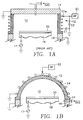
- FIG. 1A illustrates a top portion of a plasma reactor of the type disclosed in European Patent Document No. 0 520 519 A1 and in European Patent Document No. 0 552 491 A1, the disclosures of which are incorporated herein by reference.
- the plasma reactor of FIG. 1A has a generally cylindrical vacuum chamber 10, a gas inlet 11 on top of the chamber 10 for supplying a gas into the chamber interior from which a plasma is to be ignited, a cylindrical RF coil 12 wound around the exterior of the cylindrical chamber 10, a grounded top conducting lid 14 immediately above the coil 12 and a grounded side wall 16 immediately below the coil 12.
- the cylindrical RF coil 12 provides RF energy to generate a high density plasma inside the chamber 10 by inductive coupling while the conductive lid 14 is grounded to assure a grounding path for bias RF power (17) applied to a pedestal 18 supporting a semiconductor wafer 20 at the bottom of the chamber 10.
- One end 12a of the cylindrical coil 12 (e.g., the end nearest the lid) is "hot” because it is connected to the output of an RF source 22, while the opposite end is grounded.
- the coil may be a single section tapped near its center to the RF source.
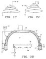
- FIG. 1B illustrates a recent variation from the apparatus of FIG. 1A in which the ceiling 14 is an insulator and both the ceiling 14 and the RF coil 12 have a dome shape, the RF coil 12 being wound in a conical helix to conform with the ceiling 14, as shown in FIG. 1C.
- the problem with the inductive RF coil having one end grounded and one end RF powered is that the RF peak-to-peak potential within the coil is very high and this causes strong capacitive coupling of RF power into the plasma.
- the high electric potential also causes a significant sputtering of chamber interior surfaces. Such sputtering is undesireable because it produces contamination harmful to the processing of the wafer.
- the RF potential within the coil also affects capacitive coupling of RF power from the coil to the wafer pedestal through the semiconductor wafer being processed.
- a high RF potential may cause a high plasma potential so as to increase the rate of physical sputtering of the wafer being processed. It is desired to control the sputtering rate of the wafer being processed by the RF bias power applied to the wafer pedestal. However, such control is distorted to a certain extent by the high capacitive coupling from the RF coil.
- the term sputtering of the wafer refers to the removal of material from the wafer through the kinetic energy of heavy ions in the plasma colliding with the material being removed. This is different from the removal of material from the wafer by etching.
- Etching involves a chemical reaction between the material being removed and chemical species in the plasma and is not primarily dependent upon kinetic energy of ions or radicals in the plasma.
- Sputtering can have beneficial uses in an etch process. For example, in etching a metal such as aluminum, alloy impurities in the aluminum (such as copper) etch very slowly relative to the aluminum and are best removed at the same rate as the aluminum by sputtering. This requires that the RF potential of the wafer pedestal be set to a level such that the sputtering rate of the copper impurity is about the same as the ethc rate of the aluminum, in this example.
- Capacitive coupling from the RF coil and RF power dissipation are advantageously reduced in the present invention by employing plural coil sections, with each coil section being connected across an RF source and being arranged so that current flow in adjacent coil sections creates magnetic fields having the same direction. Preferably, this is accomplished by winding adjacent coil sections in opposing directions while tapping the adjacent coil sections to a common point which is either the RF source or ground.
- Capacitive coupling and RF power dissipation is further reduced by employing a top lid having an outer insulating annulus and an inner conducting disk portion, the conducting disk portion being displaced or spaced apart from the coil by the width of the annulus. This displacement significantly reduces the RF power dissipation or coupling from the top winding of the coil to the lid.
- FIG. 1A is a simplified drawing of a portion of the plasma reactor of the prior art.
- FIG. 1B is a simplified drawing of a portion of a plasma reactor in accordance with a recent development having a dome ceiling and conically helical RF coil on the ceiling.
- FIG. 1C illustrates the RF coil of FIG. 1B.
- FIG. 2A is a simplified drawing of a portion of a plasma reactor embodying the present invention.
- FIG. 2B illustrates an embodiment corresponding to FIG. 2A but having a dome-shaped lid and RF coil wound thereabout.
- FIG. 2C illustrates the RF coil of FIG. 2B.
- FIG. 2D illustrates a variation of the embodiment of FIG. 2B
- FIG. 3 is a circuit diagram of a mirror coil employed in the plasma reactor of FIG. 2A.
- FIG. 4 is a detailed drawing of a preferred implementation of a conducting lid embodying one aspect of the present invention.
- FIG. 5 is a schematic diagram of a three-section coil in accordance with another embodiment of the invention.
- FIG. 6A is a graph illustrating the time domain waveform of the RF signal on the conventional RF coil of FIG. 1C and the induced capacitive RF current on the wafer pedestal prior to plasma ignition.
- FIG. 6B is a graph illustrating the time domain waveform of the RF signal on the mirror RF coil of FIG. 2C and the induced capacitive RF current on the wafer pedestal prior to plasma ignition.
- FIG. 7A is a graph illustrating the time domain waveform of the RF signal on the conventional RF coil of FIG. 1C and the induced RF current on the wafer pedestal following plasma ignition.
- FIG. 7B is a graph illustrating the time domain waveform of the RF signal on the mirror RF coil of FIG. 2B and the induced RF current on the wafer pedestal following plasma ignition.
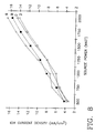
- FIG. 8 is a graph comparing the ion current density obtained with conventional RF coil of FIG. 1C with the ion current density obtained with the mirror RF coil of FIG. 2C as a function of RF power on the coil.
- FIG. 9 is a graph comparing oxide sputtering rates obtained with the conventional RF coil of FIG. 1C with the oxide sputtering rates obtained with the mirror RF coil of FIG. 2C as a function of RF power on the coil in an Ar plasma at 600 watts RF bias power on the wafer pedestal.
- RF power dissipation is advantageously reduced by a top lid 24 having an outer insulating annulus 26 and an inner conducting disk portion 28, the conducting disk portion 28 being displaced or spaced apart from the coil 12 by the width W of the annulus 26.
- This displacement reduces the RF power dissipation or coupling from the top winding of the coil 12 to the lid 24, particularly where the top end 12a of the coil is connected to the RF source 22.
- RF power dissipation is further reduced by grounding the top and bottom ends 12a, 12b of the coil 12 and connecting the RF power source to the middle 12c of the coil in a mirror configuration, as indicated in FIG. 2A and as shown more clearly in the circuit diagram of FIG. 3.
- the "hot" portion of the coil 12 is neither adjacent the grounded conductive portion 28 of the lid 24 nor the grounded lower-most portion of the side wall 16, so that RF power dissipation is reduced accordingly.
- FIG. 2B illustrates how the concept of FIG. 2A is applied to the dome-ceiling plasma reactor of FIG. 1B.
- the ceiling 14 is an insulator.
- the RF power is applied to the middle winding of the coil 12, while the two ends are grounded, as illustrated schematically in FIG. 2C.
- this feature tends to advantageously reduce capacitive coupling to the conductive cylindrical side wall 16.
- grounding the apex of the dome-shaped RF coil 12 of FIG. 2B in the manner illustrated tends to reduce capacitive coupling of the electric field between the coil and the wafer, thereby advantageously increasing inductive coupling.
- FIG. 2D illustrates how the embodiment of FIG. 2B may be modified by replacing the center of the dome 14 with the flat conductive ceiling 28 of FIG. 2A, the coil 12 having an opening therein over the center so that no coil windings overlie the conductive ceiling 28.
- the coil 12 has five windings and the power source 22 applies an RF signal of 2.0 MHz to the middle winding 12c of the coil 12, as disclosed in the above-referenced European Patent Document. Furthermore, all of the operating parameters are as disclosed in detail in the above-referenced European Patent Document and need not be reiterated herein.
- the plasma reactor of FIG. 2A processes 8-inch diameter semiconductor wafers
- the cylindrical reactor chamber 10 has a diameter of about 14 inches
- the conductive disk portion 28 has a diameter of about 8 inches so that the width W of the insulating annulus 26 is about 6 inches.
- the insulating annulus 26 is preferably made of a ceramic such as aluminum oxide or quartz while the conductive disk portion 28 and the conductive side walls 16 are made of anodized aluminum.
- the coil 12 is wound around an insulating cylindrical side wall portion 30 disposed between the lid 24 and the conductive lower portion of the side wall 16.
- the vertical height of the insulating cylindrical side wall portion 30 is about 3.75 inches.
- the insulating side wall portion is preferably made of aluminum oxide or quartz.
- FIG. 4 illustrates a preferred design of the lid 24 of FIG. 2A.
- the gas inlet 11 extends through an axial hole in the center of the conductive disk portion 28 of the lid into a gas distribution manifold of which the conductive disk portion 28 is the ceiling.
- the conductive disk portion 28 is seated on an annular ridge of the insulating annulus 26.
- FIG. 3 illustrates an embodiment in which the coil 12 constitutes two groups of coils connected in parallel to the RF source 22, RF power can be delivered to n groups of inductive coils, where n is an integer greater than 1.
- Each group of coils has a certain number of turns, which number may not be the same from group to group.
- An advantage of having more than one group of coils in the coil 12 is that capacitive coupling to the plasma is significantly reduced for a given applied RF power level as compared to a single inductive coil configuration.
- the single inductive coil configuration (corresponding to FIG.
- the RF inductive coil 12 is preferably separated into n parallel plural coil sections, where n is an integer greater than 1 (e.g., 2, 3, 4, ... etc.) as illustrated in FIGS. 2C, 3 and 5.
- n is an integer greater than 1 (e.g., 2, 3, 4, ... etc.) as illustrated in FIGS. 2C, 3 and 5.
- the RF coil 12 has a cylindrical shape, the n coil sections are mirror images of one another. In all cases it is preferable that the n coil sections are wound such that current in all sections rotates in the same direction so as to produce magnetic fields having the same direction so as to reinforce each other in inductively coupling RF power to the plasma. Preferably, this is accomplished whenever adjacent coils are connected to a common tap point (i.e., the RF source) by winding adjacent coil sections in opposite directions, as in FIGS. 2C, 3 and 5.
- a common tap point i.e., the RF source
- the lower coil section in FIG. 5 labelled “C” adjacent the coil section “B” is wound in the rotational direction of coil section "A” and is connected between the grounded lower end of coil section "B” and the common tap between coil sections "A” and "B” to which the RF source is connected.
- the plural coil sections are grouped by pairs of coil sections, each coil section being within two adjacent pairs of coil sections, each pair of coil sections having a common tap to one end of each coil section in the pair, coil sections within each of pair being wound in opposite directions, the common taps of alternate ones of the pairs being connected to the RF power terminal and the common taps of remaining ones of the pairs being connected to RF ground.
- the coil sections labelled "A” and "B” are one pair having a common tap connected to the RF source
- the coil sections labelled "B” and “C” are a second pair having a common tap connected to RF ground, the coil sections in each pair being wound in opposite rotational directions.
- FIGS. 6A and 6B indicate the induced AC voltage (waveform "A") and current (waveform "B") on the cathode or wafer pedestal in the absence of a plasma by the conventional and mirror coils, respectively, under the following conditions: chamber pressure is pumped down to the desired or baseline operating pressure, there is no gas flow and there is no plasma.
- the AC current induced on the wafer pedestal (an indicia of capacitive coupling) by the mirror coil (FIG. 6B) is lower than the AC current induced by the conventional coil (FIG. 6A).
- the absolute value is too small to measure.
- FIGS. 7A and 7B indicate the AC voltage (waveform "A") and current (waveform "B") induced on the wafer pedestal by a conventional coil and the mirror coil, respectively, with Argon gas present in the vacuum chamber and the plasma ignited.
- the AC current induced on the wafer pedestal by the mirror coil is about 15% less than that induced by the conventional coil, indicating less capacitive coupling with the mirror coil. This is a significant advantage because less capacitive coupling from the mirror coil means that more RF energy is being coupled inductively to generate a plasma with greater density, and the user is better able to control or reduce the ion energy or sputtering rate by varying RF power on the the wafer pedestal.
- the AC current measured during such tests may not necessarily arise from capacitive coupling alone, but may arise from a mixture of both capacitive and inductive coupling.
- FIG. 8 compares the ion current densities with respect to the RF power obtained from a conventional RF coil with that obtained from a mirror coil.
- the curve labelled "A” and having diamond markers represents measurements at the edge of a conventional coil.
- the curve labelled "B” and having black solid square markers represents measurements in the center of the mirror coil.
- the curve labelled "C” and having triangle markers represents measurements at the edge of the conventional coil.
- the curve labelled "D” and having white square markers represents measurements at the edge of the mirror coil. There is no noticeable difference in these measurements between the mirror coil and the conventional coil, due to large random variations. Both the conventional coil and the mirror coil are of cylindrical shapes in this comparison.
- FIG. 9 compares the oxide sputtering rate in an Argon plasma as a function of RF power obtained from a conventional RF coil with that obtained from a mirror coil.
- the curves labelled "A” and “C” with diamond and triangle markers respectively represent mearsurements from two different tests of the mirror coil.
- the curve labelled "B” with the square markers represents measurements on a conventional coil.
- a 600 Watt RF bias signal was applied to the wafer pedestal.
- the sputtering rate predominantly depends upon the RF bias power applied to the wafer pedestal, not the RF power capacitively coupled from the RF coil. Such capacitive coupling should be significantly reduced in the mirror coil, a significant advantage as explained above.
- Another advantage realized in the present invention relates to the sputtering of materials from the chamber interior surfaces. It is very common to operate the source RF power at a very high level (e.g., 2-3 kW with 5kV to 6kV peak-to-peak voltage). At such high voltage levels, the plasma tends to sputter the chamber materials at significant sputtering rates. However, the mirror coil or the plural section coil reduces the peak-to-peak voltage. This reduces the chamber material sputtering rate, thus reducing the rate of contamination of the wafer due to emanation of particles from the sputtering of the chamber wall. This also minimizes device damage on the wafer being processed resulting from such a high RF potential.
Landscapes
- Physics & Mathematics (AREA)
- Engineering & Computer Science (AREA)
- Plasma & Fusion (AREA)
- Chemical & Material Sciences (AREA)
- Analytical Chemistry (AREA)
- Plasma Technology (AREA)
- Drying Of Semiconductors (AREA)
- Physical Deposition Of Substances That Are Components Of Semiconductor Devices (AREA)
- ing And Chemical Polishing (AREA)
- Crystals, And After-Treatments Of Crystals (AREA)
Applications Claiming Priority (2)
| Application Number | Priority Date | Filing Date | Title |
|---|---|---|---|
| US08/277,531 US5540824A (en) | 1994-07-18 | 1994-07-18 | Plasma reactor with multi-section RF coil and isolated conducting lid |
| US277531 | 1994-07-18 |
Publications (3)
| Publication Number | Publication Date |
|---|---|
| EP0694949A2 true EP0694949A2 (fr) | 1996-01-31 |
| EP0694949A3 EP0694949A3 (fr) | 1998-12-16 |
| EP0694949B1 EP0694949B1 (fr) | 2001-12-19 |
Family
ID=23061269
Family Applications (1)
| Application Number | Title | Priority Date | Filing Date |
|---|---|---|---|
| EP95304041A Expired - Lifetime EP0694949B1 (fr) | 1994-07-18 | 1995-06-12 | Réacteurs à plasma à couplage inductif |
Country Status (6)
| Country | Link |
|---|---|
| US (1) | US5540824A (fr) |
| EP (1) | EP0694949B1 (fr) |
| JP (1) | JP3929514B2 (fr) |
| KR (1) | KR960005832A (fr) |
| AT (1) | ATE211304T1 (fr) |
| DE (1) | DE69524683T2 (fr) |
Cited By (17)
| Publication number | Priority date | Publication date | Assignee | Title |
|---|---|---|---|---|
| WO1997002588A1 (fr) * | 1995-06-30 | 1997-01-23 | Lam Research Corporation | Bobine a grande surface a faible inductance pour une source de plasma couplee par induction |
| EP0786804A2 (fr) | 1996-01-26 | 1997-07-30 | Applied Materials, Inc. | Appareil et méthode pour le traitement de substrats |
| WO1997033300A1 (fr) * | 1996-03-06 | 1997-09-12 | Mattson Technology, Inc. | Reacteur a plasma inductif a section generatrice de plasma de forme conique |
| EP0810816A1 (fr) * | 1996-05-30 | 1997-12-03 | Applied Materials, Inc. | Source équilibrée pour un système à plasma |
| EP0788138A3 (fr) * | 1996-02-02 | 1998-01-07 | Applied Materials, Inc. | Réacteurs à plasma pour le traitement de substrats |
| US5759280A (en) * | 1996-06-10 | 1998-06-02 | Lam Research Corporation | Inductively coupled source for deriving substantially uniform plasma flux |
| US5800619A (en) * | 1996-06-10 | 1998-09-01 | Lam Research Corporation | Vacuum plasma processor having coil with minimum magnetic field in its center |
| WO1999014784A3 (fr) * | 1997-09-16 | 1999-06-03 | Lam Res Corp | Processeur a plasma a vide comportant une bobine equipee de segments conducteurs supplementaires sur sa partie peripherique |
| US6028285A (en) * | 1997-11-19 | 2000-02-22 | Board Of Regents, The University Of Texas System | High density plasma source for semiconductor processing |
| EP1079671A3 (fr) * | 1999-08-26 | 2001-11-07 | Jusung Engineering Co. Ltd. | Dispositif d'antenne pour engendrer un plasma à couplage inductif |
| EP1047289A3 (fr) * | 1999-04-22 | 2004-01-02 | Applied Materials, Inc. | Source de plasma à radiofréquence pour traitement de materiaux |
| US6736931B2 (en) | 1991-06-27 | 2004-05-18 | Kenneth S. Collins | Inductively coupled RF plasma reactor and plasma chamber enclosure structure therefor |
| US6790375B1 (en) | 1998-09-30 | 2004-09-14 | Lam Research Corporation | Dechucking method and apparatus for workpieces in vacuum processors |
| US6965506B2 (en) | 1998-09-30 | 2005-11-15 | Lam Research Corporation | System and method for dechucking a workpiece from an electrostatic chuck |
| DE19781667B4 (de) * | 1996-03-27 | 2007-07-05 | Tokyo Electron Ltd. | Plasmaerzeugungsverfahren und -gerät mit einer induktiv gekoppelten Plasmaquelle |
| EP1608000A3 (fr) * | 1996-06-10 | 2007-11-28 | Lam Research Corporation | Processeur de plasma RF |
| CN102056393A (zh) * | 2009-10-26 | 2011-05-11 | 应用材料股份有限公司 | 电感耦合等离子体反应器 |
Families Citing this family (60)
| Publication number | Priority date | Publication date | Assignee | Title |
|---|---|---|---|---|
| JP3105403B2 (ja) * | 1994-09-14 | 2000-10-30 | 松下電器産業株式会社 | プラズマ処理装置 |
| EP0710055B1 (fr) | 1994-10-31 | 1999-06-23 | Applied Materials, Inc. | Réacteurs à plasma pour le traitement de plaquettes semi-conductrices |
| US5643639A (en) * | 1994-12-22 | 1997-07-01 | Research Triangle Institute | Plasma treatment method for treatment of a large-area work surface apparatus and methods |
| US5688357A (en) * | 1995-02-15 | 1997-11-18 | Applied Materials, Inc. | Automatic frequency tuning of an RF power source of an inductively coupled plasma reactor |
| US6132564A (en) * | 1997-11-17 | 2000-10-17 | Tokyo Electron Limited | In-situ pre-metallization clean and metallization of semiconductor wafers |
| US6224724B1 (en) | 1995-02-23 | 2001-05-01 | Tokyo Electron Limited | Physical vapor processing of a surface with non-uniformity compensation |
| US5907221A (en) * | 1995-08-16 | 1999-05-25 | Applied Materials, Inc. | Inductively coupled plasma reactor with an inductive coil antenna having independent loops |
| US6264812B1 (en) | 1995-11-15 | 2001-07-24 | Applied Materials, Inc. | Method and apparatus for generating a plasma |
| US5900105A (en) * | 1996-07-09 | 1999-05-04 | Gamma Precision Technology, Inc. | Wafer transfer system and method of using the same |
| US5846883A (en) * | 1996-07-10 | 1998-12-08 | Cvc, Inc. | Method for multi-zone high-density inductively-coupled plasma generation |
| US6254737B1 (en) | 1996-10-08 | 2001-07-03 | Applied Materials, Inc. | Active shield for generating a plasma for sputtering |
| US6190513B1 (en) | 1997-05-14 | 2001-02-20 | Applied Materials, Inc. | Darkspace shield for improved RF transmission in inductively coupled plasma sources for sputter deposition |
| TW403959B (en) * | 1996-11-27 | 2000-09-01 | Hitachi Ltd | Plasma treatment device |
| US5948215A (en) * | 1997-04-21 | 1999-09-07 | Tokyo Electron Limited | Method and apparatus for ionized sputtering |
| US5800688A (en) * | 1997-04-21 | 1998-09-01 | Tokyo Electron Limited | Apparatus for ionized sputtering |
| US6178920B1 (en) | 1997-06-05 | 2001-01-30 | Applied Materials, Inc. | Plasma reactor with internal inductive antenna capable of generating helicon wave |
| US6158384A (en) * | 1997-06-05 | 2000-12-12 | Applied Materials, Inc. | Plasma reactor with multiple small internal inductive antennas |
| US6565717B1 (en) | 1997-09-15 | 2003-05-20 | Applied Materials, Inc. | Apparatus for sputtering ionized material in a medium to high density plasma |
| US6132566A (en) * | 1998-07-30 | 2000-10-17 | Applied Materials, Inc. | Apparatus and method for sputtering ionized material in a plasma |
| US6523493B1 (en) * | 2000-08-01 | 2003-02-25 | Tokyo Electron Limited | Ring-shaped high-density plasma source and method |
| US6192829B1 (en) | 1999-05-05 | 2001-02-27 | Applied Materials, Inc. | Antenna coil assemblies for substrate processing chambers |
| JP2001052894A (ja) * | 1999-08-04 | 2001-02-23 | Ulvac Japan Ltd | 誘導結合高周波プラズマ源 |
| SE9903675D0 (sv) * | 1999-10-13 | 1999-10-13 | Abb Research Ltd | A device and a method for heat treatment of an object in a susceptor |
| US6447636B1 (en) * | 2000-02-16 | 2002-09-10 | Applied Materials, Inc. | Plasma reactor with dynamic RF inductive and capacitive coupling control |
| US6694915B1 (en) * | 2000-07-06 | 2004-02-24 | Applied Materials, Inc | Plasma reactor having a symmetrical parallel conductor coil antenna |
| US6414648B1 (en) | 2000-07-06 | 2002-07-02 | Applied Materials, Inc. | Plasma reactor having a symmetric parallel conductor coil antenna |
| US6685798B1 (en) | 2000-07-06 | 2004-02-03 | Applied Materials, Inc | Plasma reactor having a symmetrical parallel conductor coil antenna |
| US6409933B1 (en) | 2000-07-06 | 2002-06-25 | Applied Materials, Inc. | Plasma reactor having a symmetric parallel conductor coil antenna |
| US6459066B1 (en) | 2000-08-25 | 2002-10-01 | Board Of Regents, The University Of Texas System | Transmission line based inductively coupled plasma source with stable impedance |
| US6875700B2 (en) * | 2000-08-29 | 2005-04-05 | Board Of Regents, The University Of Texas System | Ion-Ion plasma processing with bias modulation synchronized to time-modulated discharges |
| KR100469889B1 (ko) * | 2002-11-14 | 2005-02-02 | 어댑티브프라즈마테크놀로지 주식회사 | 복수개의 코일들을 포함하는 플라즈마 식각 설비 |
| JP2003282547A (ja) * | 2002-03-26 | 2003-10-03 | Ulvac Japan Ltd | 高選択比かつ大面積高均一プラズマ処理方法及び装置 |
| DE10231739B4 (de) * | 2002-07-13 | 2004-10-28 | Deutsches Zentrum für Luft- und Raumfahrt e.V. | Induktions-Plasmabrennervorrichtung |
| DE10231738B4 (de) * | 2002-07-13 | 2005-03-17 | Deutsches Zentrum für Luft- und Raumfahrt e.V. | Anpassungsvorrichtung für eine Induktions-Plasmabrennervorrichtung und Verfahren zur elektrischen Steuerung und Regelung einer Induktions-Plasmabrennervorrichtung |
| KR100964398B1 (ko) | 2003-01-03 | 2010-06-17 | 삼성전자주식회사 | 유도결합형 안테나 및 이를 채용한 플라즈마 처리장치 |
| KR100561848B1 (ko) * | 2003-11-04 | 2006-03-16 | 삼성전자주식회사 | 헬리컬 공진기형 플라즈마 처리 장치 |
| US20050145341A1 (en) * | 2003-11-19 | 2005-07-07 | Masaki Suzuki | Plasma processing apparatus |
| KR101038204B1 (ko) * | 2004-02-25 | 2011-05-31 | 주성엔지니어링(주) | 플라즈마 발생용 안테나 |
| US20050205211A1 (en) * | 2004-03-22 | 2005-09-22 | Vikram Singh | Plasma immersion ion implantion apparatus and method |
| KR100876050B1 (ko) * | 2004-12-28 | 2008-12-26 | 가부시키가이샤 히다치 고쿠사이 덴키 | 기판 처리 장치 |
| US8187416B2 (en) * | 2005-05-20 | 2012-05-29 | Applied Materials, Inc. | Interior antenna for substrate processing chamber |
| KR100785401B1 (ko) * | 2005-11-04 | 2007-12-13 | 세메스 주식회사 | 유도 결합형 플라즈마 처리 장치 |
| US20070170867A1 (en) * | 2006-01-24 | 2007-07-26 | Varian Semiconductor Equipment Associates, Inc. | Plasma Immersion Ion Source With Low Effective Antenna Voltage |
| US20080132046A1 (en) * | 2006-12-04 | 2008-06-05 | Varian Semiconductor Equipment Associates, Inc. | Plasma Doping With Electronically Controllable Implant Angle |
| US20080169183A1 (en) * | 2007-01-16 | 2008-07-17 | Varian Semiconductor Equipment Associates, Inc. | Plasma Source with Liner for Reducing Metal Contamination |
| US7820533B2 (en) * | 2007-02-16 | 2010-10-26 | Varian Semiconductor Equipment Associates, Inc. | Multi-step plasma doping with improved dose control |
| JP5410950B2 (ja) * | 2009-01-15 | 2014-02-05 | 株式会社日立ハイテクノロジーズ | プラズマ処理装置 |
| JP5572329B2 (ja) * | 2009-01-15 | 2014-08-13 | 株式会社日立ハイテクノロジーズ | プラズマ処理装置およびプラズマ生成装置 |
| JP6101031B2 (ja) * | 2012-09-28 | 2017-03-22 | 東京応化工業株式会社 | プラズマ処理装置および積層体の製造方法 |
| US8970114B2 (en) | 2013-02-01 | 2015-03-03 | Lam Research Corporation | Temperature controlled window of a plasma processing chamber component |
| WO2015067298A1 (fr) * | 2013-11-05 | 2015-05-14 | Applied Materials, Inc. | Radiofréquence (rf) - source de dépôt par pulvérisation, appareil de dépôt et son procédé d'assemblage |
| US10187966B2 (en) * | 2015-07-24 | 2019-01-22 | Applied Materials, Inc. | Method and apparatus for gas abatement |
| KR102026880B1 (ko) * | 2016-10-13 | 2019-09-30 | 에이피시스템 주식회사 | 기판 처리 장치 |
| CN107256822B (zh) * | 2017-07-27 | 2019-08-23 | 北京北方华创微电子装备有限公司 | 上电极组件及反应腔室 |
| CN108770173B (zh) * | 2018-07-27 | 2020-11-20 | 上海工程技术大学 | 一种等离子体射流产生装置 |
| KR20210039451A (ko) * | 2018-09-20 | 2021-04-09 | 가부시키가이샤 코쿠사이 엘렉트릭 | 기판 처리 장치, 반도체 장치의 제조 방법 및 프로그램 |
| DE102019213591A1 (de) * | 2019-09-06 | 2021-03-11 | Singulus Technologies Ag | Behandlungsanlage und plasmabehandlungsverfahren |
| FR3135731B1 (fr) * | 2022-05-17 | 2024-04-12 | Univ Grenoble Alpes | Procédé de dépôt de couches atomiques assisté par plasma à couplage capacitif |
| FR3135732B1 (fr) * | 2022-05-17 | 2024-04-12 | Univ Grenoble Alpes | Réacteur de dépôt assisté par plasma |
| CN120530475A (zh) * | 2022-12-21 | 2025-08-22 | 朗姆研究公司 | 具有并联螺旋rf线圈的感应耦合等离子体源 |
Citations (3)
| Publication number | Priority date | Publication date | Assignee | Title |
|---|---|---|---|---|
| US4948458A (en) | 1989-08-14 | 1990-08-14 | Lam Research Corporation | Method and apparatus for producing magnetically-coupled planar plasma |
| EP0520519A1 (fr) | 1991-06-27 | 1992-12-30 | Applied Materials, Inc. | Réacteurs de traitement par plasma et procédé de gravure par plasma |
| EP0552491A1 (fr) | 1992-01-24 | 1993-07-28 | Applied Materials, Inc. | Procédé de gravure par plasma |
Family Cites Families (19)
| Publication number | Priority date | Publication date | Assignee | Title |
|---|---|---|---|---|
| US4464223A (en) * | 1983-10-03 | 1984-08-07 | Tegal Corp. | Plasma reactor apparatus and method |
| KR900007687B1 (ko) * | 1986-10-17 | 1990-10-18 | 가부시기가이샤 히다찌세이사꾸쇼 | 플라즈마처리방법 및 장치 |
| GB8629634D0 (en) * | 1986-12-11 | 1987-01-21 | Dobson C D | Reactive ion & sputter etching |
| US4872947A (en) * | 1986-12-19 | 1989-10-10 | Applied Materials, Inc. | CVD of silicon oxide using TEOS decomposition and in-situ planarization process |
| US4842683A (en) * | 1986-12-19 | 1989-06-27 | Applied Materials, Inc. | Magnetic field-enhanced plasma etch reactor |
| DE3738352A1 (de) * | 1987-11-11 | 1989-05-24 | Technics Plasma Gmbh | Filamentloses magnetron-ionenstrahlsystem |
| US4918031A (en) * | 1988-12-28 | 1990-04-17 | American Telephone And Telegraph Company,At&T Bell Laboratories | Processes depending on plasma generation using a helical resonator |
| EP0379828B1 (fr) * | 1989-01-25 | 1995-09-27 | International Business Machines Corporation | Dispositif de traitement par plasma multipolaire à induction de radiofréquence |
| GB8905075D0 (en) * | 1989-03-06 | 1989-04-19 | Nordiko Ltd | Electrode assembly and apparatus |
| US5122251A (en) * | 1989-06-13 | 1992-06-16 | Plasma & Materials Technologies, Inc. | High density plasma deposition and etching apparatus |
| WO1991010341A1 (fr) * | 1990-01-04 | 1991-07-11 | Savas Stephen E | Reacteur a plasma hf inductif a basse frequence |
| EP0468742B1 (fr) * | 1990-07-24 | 1996-03-27 | Varian Australia Pty. Ltd. | Spectroscopie utilisant un plasma à couplage inductif |
| JP3670277B2 (ja) * | 1991-05-17 | 2005-07-13 | ラム リサーチ コーポレーション | 低い固有応力および/または低い水素含有率をもつSiO▲X▼フィルムの堆積法 |
| US5234529A (en) * | 1991-10-10 | 1993-08-10 | Johnson Wayne L | Plasma generating apparatus employing capacitive shielding and process for using such apparatus |
| US5280154A (en) * | 1992-01-30 | 1994-01-18 | International Business Machines Corporation | Radio frequency induction plasma processing system utilizing a uniform field coil |
| US5241245A (en) * | 1992-05-06 | 1993-08-31 | International Business Machines Corporation | Optimized helical resonator for plasma processing |
| US5226967A (en) * | 1992-05-14 | 1993-07-13 | Lam Research Corporation | Plasma apparatus including dielectric window for inducing a uniform electric field in a plasma chamber |
| US5277751A (en) * | 1992-06-18 | 1994-01-11 | Ogle John S | Method and apparatus for producing low pressure planar plasma using a coil with its axis parallel to the surface of a coupling window |
| US5346578A (en) * | 1992-11-04 | 1994-09-13 | Novellus Systems, Inc. | Induction plasma source |
-
1994
- 1994-07-18 US US08/277,531 patent/US5540824A/en not_active Expired - Lifetime
-
1995
- 1995-06-12 EP EP95304041A patent/EP0694949B1/fr not_active Expired - Lifetime
- 1995-06-12 AT AT95304041T patent/ATE211304T1/de not_active IP Right Cessation
- 1995-06-12 DE DE69524683T patent/DE69524683T2/de not_active Expired - Fee Related
- 1995-07-18 JP JP18154495A patent/JP3929514B2/ja not_active Expired - Fee Related
- 1995-07-18 KR KR19950020962A patent/KR960005832A/ko not_active Abandoned
Patent Citations (3)
| Publication number | Priority date | Publication date | Assignee | Title |
|---|---|---|---|---|
| US4948458A (en) | 1989-08-14 | 1990-08-14 | Lam Research Corporation | Method and apparatus for producing magnetically-coupled planar plasma |
| EP0520519A1 (fr) | 1991-06-27 | 1992-12-30 | Applied Materials, Inc. | Réacteurs de traitement par plasma et procédé de gravure par plasma |
| EP0552491A1 (fr) | 1992-01-24 | 1993-07-28 | Applied Materials, Inc. | Procédé de gravure par plasma |
Cited By (26)
| Publication number | Priority date | Publication date | Assignee | Title |
|---|---|---|---|---|
| US6736931B2 (en) | 1991-06-27 | 2004-05-18 | Kenneth S. Collins | Inductively coupled RF plasma reactor and plasma chamber enclosure structure therefor |
| US6248250B1 (en) | 1995-02-15 | 2001-06-19 | Applied Materials Inc. | RF plasma reactor with hybrid conductor and multi-radius dome ceiling |
| US6184488B1 (en) | 1995-06-30 | 2001-02-06 | Lam Research Corporation | Low inductance large area coil for an inductively coupled plasma source |
| WO1997002588A1 (fr) * | 1995-06-30 | 1997-01-23 | Lam Research Corporation | Bobine a grande surface a faible inductance pour une source de plasma couplee par induction |
| US5874704A (en) * | 1995-06-30 | 1999-02-23 | Lam Research Corporation | Low inductance large area coil for an inductively coupled plasma source |
| EP0786804A2 (fr) | 1996-01-26 | 1997-07-30 | Applied Materials, Inc. | Appareil et méthode pour le traitement de substrats |
| EP0788138A3 (fr) * | 1996-02-02 | 1998-01-07 | Applied Materials, Inc. | Réacteurs à plasma pour le traitement de substrats |
| WO1997033300A1 (fr) * | 1996-03-06 | 1997-09-12 | Mattson Technology, Inc. | Reacteur a plasma inductif a section generatrice de plasma de forme conique |
| US5964949A (en) * | 1996-03-06 | 1999-10-12 | Mattson Technology, Inc. | ICP reactor having a conically-shaped plasma-generating section |
| DE19781667B4 (de) * | 1996-03-27 | 2007-07-05 | Tokyo Electron Ltd. | Plasmaerzeugungsverfahren und -gerät mit einer induktiv gekoppelten Plasmaquelle |
| EP0810816A1 (fr) * | 1996-05-30 | 1997-12-03 | Applied Materials, Inc. | Source équilibrée pour un système à plasma |
| US6353206B1 (en) | 1996-05-30 | 2002-03-05 | Applied Materials, Inc. | Plasma system with a balanced source |
| US5800619A (en) * | 1996-06-10 | 1998-09-01 | Lam Research Corporation | Vacuum plasma processor having coil with minimum magnetic field in its center |
| US6027603A (en) * | 1996-06-10 | 2000-02-22 | Lam Research Corporation | Inductively coupled planar source for substantially uniform plasma flux |
| EP1608000A3 (fr) * | 1996-06-10 | 2007-11-28 | Lam Research Corporation | Processeur de plasma RF |
| US5759280A (en) * | 1996-06-10 | 1998-06-02 | Lam Research Corporation | Inductively coupled source for deriving substantially uniform plasma flux |
| US6028395A (en) * | 1997-09-16 | 2000-02-22 | Lam Research Corporation | Vacuum plasma processor having coil with added conducting segments to its peripheral part |
| WO1999014784A3 (fr) * | 1997-09-16 | 1999-06-03 | Lam Res Corp | Processeur a plasma a vide comportant une bobine equipee de segments conducteurs supplementaires sur sa partie peripherique |
| US6028285A (en) * | 1997-11-19 | 2000-02-22 | Board Of Regents, The University Of Texas System | High density plasma source for semiconductor processing |
| US6790375B1 (en) | 1998-09-30 | 2004-09-14 | Lam Research Corporation | Dechucking method and apparatus for workpieces in vacuum processors |
| US6965506B2 (en) | 1998-09-30 | 2005-11-15 | Lam Research Corporation | System and method for dechucking a workpiece from an electrostatic chuck |
| EP1047289A3 (fr) * | 1999-04-22 | 2004-01-02 | Applied Materials, Inc. | Source de plasma à radiofréquence pour traitement de materiaux |
| EP1079671A3 (fr) * | 1999-08-26 | 2001-11-07 | Jusung Engineering Co. Ltd. | Dispositif d'antenne pour engendrer un plasma à couplage inductif |
| CN102056393A (zh) * | 2009-10-26 | 2011-05-11 | 应用材料股份有限公司 | 电感耦合等离子体反应器 |
| CN102056393B (zh) * | 2009-10-26 | 2016-01-20 | 应用材料公司 | 电感耦合等离子体反应器 |
| US10573493B2 (en) | 2009-10-26 | 2020-02-25 | Applied Materials, Inc. | Inductively coupled plasma apparatus |
Also Published As
| Publication number | Publication date |
|---|---|
| JPH08213196A (ja) | 1996-08-20 |
| JP3929514B2 (ja) | 2007-06-13 |
| DE69524683T2 (de) | 2002-08-08 |
| ATE211304T1 (de) | 2002-01-15 |
| DE69524683D1 (de) | 2002-01-31 |
| EP0694949B1 (fr) | 2001-12-19 |
| KR960005832A (fr) | 1996-02-23 |
| EP0694949A3 (fr) | 1998-12-16 |
| US5540824A (en) | 1996-07-30 |
Similar Documents
| Publication | Publication Date | Title |
|---|---|---|
| US5540824A (en) | Plasma reactor with multi-section RF coil and isolated conducting lid | |
| KR100328135B1 (ko) | 플라즈마점화를향상시키기위한전극을가지는유도결합된플라즈마반응로 | |
| KR100440236B1 (ko) | 플라즈마 처리 장치 | |
| KR100417327B1 (ko) | 진공플라즈마프로세서 | |
| US6030667A (en) | Apparatus and method for applying RF power apparatus and method for generating plasma and apparatus and method for processing with plasma | |
| US5759280A (en) | Inductively coupled source for deriving substantially uniform plasma flux | |
| US5998933A (en) | RF plasma inductor with closed ferrite core | |
| JP2613002B2 (ja) | 共振器 | |
| US7426900B2 (en) | Integrated electrostatic inductive coupling for plasma processing | |
| US7854213B2 (en) | Modulated gap segmented antenna for inductively-coupled plasma processing system | |
| KR100444189B1 (ko) | 유도결합 플라즈마 소스의 임피던스 정합 회로 | |
| US5669975A (en) | Plasma producing method and apparatus including an inductively-coupled plasma source | |
| US5231334A (en) | Plasma source and method of manufacturing | |
| KR100474752B1 (ko) | 전기적으로가변가능한밀도분포를갖는플라즈마소스 | |
| US7771562B2 (en) | Etch system with integrated inductive coupling | |
| JPH08339897A (ja) | 誘導プラズマ発生装置および容量結合を与える方法 | |
| JPH02235332A (ja) | プラズマ処理装置 | |
| JPH08195297A (ja) | プラズマ処理箱内に誘導的に結合されたプラズマ発生源を組み入れるための構造並びに方法 | |
| KR20050106409A (ko) | 플라즈마 챔버에서 이온 폭격 에너지를 최소화하는메커니즘 | |
| KR20010096474A (ko) | 플라즈마 에칭 장치 | |
| TW557643B (en) | Inductively coupled plasma processor | |
| JPH0850998A (ja) | プラズマ処理装置 | |
| KR100506561B1 (ko) | 유도결합식플라즈마소스를포함하는플라즈마발생방법및장치 | |
| KR100488362B1 (ko) | 저주파형 유도결합 플라즈마 발생장치 | |
| JP3017021U (ja) | 誘導結合プラズマ発生用コイル |
Legal Events
| Date | Code | Title | Description |
|---|---|---|---|
| PUAI | Public reference made under article 153(3) epc to a published international application that has entered the european phase |
Free format text: ORIGINAL CODE: 0009012 |
|
| AK | Designated contracting states |
Kind code of ref document: A2 Designated state(s): AT BE CH DE ES FR GB GR IE IT LI NL SE |
|
| PUAL | Search report despatched |
Free format text: ORIGINAL CODE: 0009013 |
|
| AK | Designated contracting states |
Kind code of ref document: A3 Designated state(s): AT BE CH DE ES FR GB GR IE IT LI NL SE |
|
| 17P | Request for examination filed |
Effective date: 19990615 |
|
| 17Q | First examination report despatched |
Effective date: 19991117 |
|
| GRAG | Despatch of communication of intention to grant |
Free format text: ORIGINAL CODE: EPIDOS AGRA |
|
| GRAG | Despatch of communication of intention to grant |
Free format text: ORIGINAL CODE: EPIDOS AGRA |
|
| GRAG | Despatch of communication of intention to grant |
Free format text: ORIGINAL CODE: EPIDOS AGRA |
|
| GRAH | Despatch of communication of intention to grant a patent |
Free format text: ORIGINAL CODE: EPIDOS IGRA |
|
| GRAH | Despatch of communication of intention to grant a patent |
Free format text: ORIGINAL CODE: EPIDOS IGRA |
|
| GRAA | (expected) grant |
Free format text: ORIGINAL CODE: 0009210 |
|
| AK | Designated contracting states |
Kind code of ref document: B1 Designated state(s): AT BE CH DE ES FR GB GR IE IT LI NL SE |
|
| PG25 | Lapsed in a contracting state [announced via postgrant information from national office to epo] |
Ref country code: NL Free format text: LAPSE BECAUSE OF FAILURE TO SUBMIT A TRANSLATION OF THE DESCRIPTION OR TO PAY THE FEE WITHIN THE PRESCRIBED TIME-LIMIT Effective date: 20011219 Ref country code: LI Free format text: LAPSE BECAUSE OF FAILURE TO SUBMIT A TRANSLATION OF THE DESCRIPTION OR TO PAY THE FEE WITHIN THE PRESCRIBED TIME-LIMIT Effective date: 20011219 Ref country code: GR Free format text: LAPSE BECAUSE OF FAILURE TO SUBMIT A TRANSLATION OF THE DESCRIPTION OR TO PAY THE FEE WITHIN THE PRESCRIBED TIME-LIMIT Effective date: 20011219 Ref country code: CH Free format text: LAPSE BECAUSE OF FAILURE TO SUBMIT A TRANSLATION OF THE DESCRIPTION OR TO PAY THE FEE WITHIN THE PRESCRIBED TIME-LIMIT Effective date: 20011219 Ref country code: BE Free format text: LAPSE BECAUSE OF FAILURE TO SUBMIT A TRANSLATION OF THE DESCRIPTION OR TO PAY THE FEE WITHIN THE PRESCRIBED TIME-LIMIT Effective date: 20011219 Ref country code: AT Free format text: LAPSE BECAUSE OF FAILURE TO SUBMIT A TRANSLATION OF THE DESCRIPTION OR TO PAY THE FEE WITHIN THE PRESCRIBED TIME-LIMIT Effective date: 20011219 |
|
| REF | Corresponds to: |
Ref document number: 211304 Country of ref document: AT Date of ref document: 20020115 Kind code of ref document: T |
|
| REG | Reference to a national code |
Ref country code: CH Ref legal event code: EP |
|
| REG | Reference to a national code |
Ref country code: GB Ref legal event code: IF02 |
|
| REG | Reference to a national code |
Ref country code: IE Ref legal event code: FG4D |
|
| REF | Corresponds to: |
Ref document number: 69524683 Country of ref document: DE Date of ref document: 20020131 |
|
| PG25 | Lapsed in a contracting state [announced via postgrant information from national office to epo] |
Ref country code: SE Free format text: LAPSE BECAUSE OF FAILURE TO SUBMIT A TRANSLATION OF THE DESCRIPTION OR TO PAY THE FEE WITHIN THE PRESCRIBED TIME-LIMIT Effective date: 20020319 |
|
| NLV1 | Nl: lapsed or annulled due to failure to fulfill the requirements of art. 29p and 29m of the patents act | ||
| ET | Fr: translation filed | ||
| PG25 | Lapsed in a contracting state [announced via postgrant information from national office to epo] |
Ref country code: ES Free format text: LAPSE BECAUSE OF FAILURE TO SUBMIT A TRANSLATION OF THE DESCRIPTION OR TO PAY THE FEE WITHIN THE PRESCRIBED TIME-LIMIT Effective date: 20020627 |
|
| REG | Reference to a national code |
Ref country code: CH Ref legal event code: PL |
|
| PLBE | No opposition filed within time limit |
Free format text: ORIGINAL CODE: 0009261 |
|
| STAA | Information on the status of an ep patent application or granted ep patent |
Free format text: STATUS: NO OPPOSITION FILED WITHIN TIME LIMIT |
|
| 26N | No opposition filed | ||
| PGFP | Annual fee paid to national office [announced via postgrant information from national office to epo] |
Ref country code: FR Payment date: 20030530 Year of fee payment: 9 |
|
| NLV1 | Nl: lapsed or annulled due to failure to fulfill the requirements of art. 29p and 29m of the patents act | ||
| PGFP | Annual fee paid to national office [announced via postgrant information from national office to epo] |
Ref country code: IE Payment date: 20030611 Year of fee payment: 9 |
|
| PGFP | Annual fee paid to national office [announced via postgrant information from national office to epo] |
Ref country code: DE Payment date: 20030828 Year of fee payment: 9 |
|
| PG25 | Lapsed in a contracting state [announced via postgrant information from national office to epo] |
Ref country code: IE Free format text: LAPSE BECAUSE OF NON-PAYMENT OF DUE FEES Effective date: 20040614 |
|
| PG25 | Lapsed in a contracting state [announced via postgrant information from national office to epo] |
Ref country code: DE Free format text: LAPSE BECAUSE OF NON-PAYMENT OF DUE FEES Effective date: 20050101 |
|
| PG25 | Lapsed in a contracting state [announced via postgrant information from national office to epo] |
Ref country code: FR Free format text: LAPSE BECAUSE OF NON-PAYMENT OF DUE FEES Effective date: 20050228 |
|
| REG | Reference to a national code |
Ref country code: IE Ref legal event code: MM4A |
|
| REG | Reference to a national code |
Ref country code: FR Ref legal event code: ST |
|
| PGFP | Annual fee paid to national office [announced via postgrant information from national office to epo] |
Ref country code: GB Payment date: 20050506 Year of fee payment: 11 |
|
| PG25 | Lapsed in a contracting state [announced via postgrant information from national office to epo] |
Ref country code: IT Free format text: LAPSE BECAUSE OF NON-PAYMENT OF DUE FEES;WARNING: LAPSES OF ITALIAN PATENTS WITH EFFECTIVE DATE BEFORE 2007 MAY HAVE OCCURRED AT ANY TIME BEFORE 2007. THE CORRECT EFFECTIVE DATE MAY BE DIFFERENT FROM THE ONE RECORDED. Effective date: 20050612 |
|
| PG25 | Lapsed in a contracting state [announced via postgrant information from national office to epo] |
Ref country code: GB Free format text: LAPSE BECAUSE OF NON-PAYMENT OF DUE FEES Effective date: 20060612 |
|
| GBPC | Gb: european patent ceased through non-payment of renewal fee |
Effective date: 20060612 |