EP0694968A2 - Halbleiter-Multichip-Baustein - Google Patents
Halbleiter-Multichip-Baustein Download PDFInfo
- Publication number
- EP0694968A2 EP0694968A2 EP95111789A EP95111789A EP0694968A2 EP 0694968 A2 EP0694968 A2 EP 0694968A2 EP 95111789 A EP95111789 A EP 95111789A EP 95111789 A EP95111789 A EP 95111789A EP 0694968 A2 EP0694968 A2 EP 0694968A2
- Authority
- EP
- European Patent Office
- Prior art keywords
- base board
- semiconductor device
- chip
- chips
- chip module
- Prior art date
- Legal status (The legal status is an assumption and is not a legal conclusion. Google has not performed a legal analysis and makes no representation as to the accuracy of the status listed.)
- Withdrawn
Links
Images



Classifications
-
- H—ELECTRICITY
- H10—SEMICONDUCTOR DEVICES; ELECTRIC SOLID-STATE DEVICES NOT OTHERWISE PROVIDED FOR
- H10W—GENERIC PACKAGES, INTERCONNECTIONS, CONNECTORS OR OTHER CONSTRUCTIONAL DETAILS OF DEVICES COVERED BY CLASS H10
- H10W70/00—Package substrates; Interposers; Redistribution layers [RDL]
- H10W70/60—Insulating or insulated package substrates; Interposers; Redistribution layers
- H10W70/67—Insulating or insulated package substrates; Interposers; Redistribution layers characterised by their insulating layers or insulating parts
- H10W70/688—Flexible insulating substrates
-
- H—ELECTRICITY
- H05—ELECTRIC TECHNIQUES NOT OTHERWISE PROVIDED FOR
- H05K—PRINTED CIRCUITS; CASINGS OR CONSTRUCTIONAL DETAILS OF ELECTRIC APPARATUS; MANUFACTURE OF ASSEMBLAGES OF ELECTRICAL COMPONENTS
- H05K1/00—Printed circuits
- H05K1/02—Details
- H05K1/0201—Thermal arrangements, e.g. for cooling, heating or preventing overheating
- H05K1/0203—Cooling of mounted components
- H05K1/0204—Cooling of mounted components using means for thermal conduction connection in the thickness direction of the substrate
-
- H—ELECTRICITY
- H10—SEMICONDUCTOR DEVICES; ELECTRIC SOLID-STATE DEVICES NOT OTHERWISE PROVIDED FOR
- H10W—GENERIC PACKAGES, INTERCONNECTIONS, CONNECTORS OR OTHER CONSTRUCTIONAL DETAILS OF DEVICES COVERED BY CLASS H10
- H10W40/00—Arrangements for thermal protection or thermal control
- H10W40/20—Arrangements for cooling
- H10W40/22—Arrangements for cooling characterised by their shape, e.g. having conical or cylindrical projections
-
- H—ELECTRICITY
- H10—SEMICONDUCTOR DEVICES; ELECTRIC SOLID-STATE DEVICES NOT OTHERWISE PROVIDED FOR
- H10W—GENERIC PACKAGES, INTERCONNECTIONS, CONNECTORS OR OTHER CONSTRUCTIONAL DETAILS OF DEVICES COVERED BY CLASS H10
- H10W90/00—Package configurations
-
- H—ELECTRICITY
- H05—ELECTRIC TECHNIQUES NOT OTHERWISE PROVIDED FOR
- H05K—PRINTED CIRCUITS; CASINGS OR CONSTRUCTIONAL DETAILS OF ELECTRIC APPARATUS; MANUFACTURE OF ASSEMBLAGES OF ELECTRICAL COMPONENTS
- H05K1/00—Printed circuits
- H05K1/02—Details
- H05K1/14—Structural association of two or more printed circuits
- H05K1/141—One or more single auxiliary printed circuits mounted on a main printed circuit, e.g. modules, adapters
-
- H—ELECTRICITY
- H05—ELECTRIC TECHNIQUES NOT OTHERWISE PROVIDED FOR
- H05K—PRINTED CIRCUITS; CASINGS OR CONSTRUCTIONAL DETAILS OF ELECTRIC APPARATUS; MANUFACTURE OF ASSEMBLAGES OF ELECTRICAL COMPONENTS
- H05K1/00—Printed circuits
- H05K1/18—Printed circuits structurally associated with non-printed electric components
- H05K1/182—Printed circuits structurally associated with non-printed electric components associated with components mounted in printed circuit boards [PCB], e.g. insert-mounted components [IMC]
-
- H—ELECTRICITY
- H05—ELECTRIC TECHNIQUES NOT OTHERWISE PROVIDED FOR
- H05K—PRINTED CIRCUITS; CASINGS OR CONSTRUCTIONAL DETAILS OF ELECTRIC APPARATUS; MANUFACTURE OF ASSEMBLAGES OF ELECTRICAL COMPONENTS
- H05K2201/00—Indexing scheme relating to printed circuits covered by H05K1/00
- H05K2201/09—Shape and layout
- H05K2201/09009—Substrate related
- H05K2201/09054—Raised area or protrusion of metal substrate
-
- H—ELECTRICITY
- H05—ELECTRIC TECHNIQUES NOT OTHERWISE PROVIDED FOR
- H05K—PRINTED CIRCUITS; CASINGS OR CONSTRUCTIONAL DETAILS OF ELECTRIC APPARATUS; MANUFACTURE OF ASSEMBLAGES OF ELECTRICAL COMPONENTS
- H05K2201/00—Indexing scheme relating to printed circuits covered by H05K1/00
- H05K2201/10—Details of components or other objects attached to or integrated in a printed circuit board
- H05K2201/10227—Other objects, e.g. metallic pieces
- H05K2201/10416—Metallic blocks or heatsinks completely inserted in a PCB
-
- H—ELECTRICITY
- H10—SEMICONDUCTOR DEVICES; ELECTRIC SOLID-STATE DEVICES NOT OTHERWISE PROVIDED FOR
- H10W—GENERIC PACKAGES, INTERCONNECTIONS, CONNECTORS OR OTHER CONSTRUCTIONAL DETAILS OF DEVICES COVERED BY CLASS H10
- H10W72/00—Interconnections or connectors in packages
- H10W72/071—Connecting or disconnecting
- H10W72/072—Connecting or disconnecting of bump connectors
- H10W72/07251—Connecting or disconnecting of bump connectors characterised by changes in properties of the bump connectors during connecting
-
- H—ELECTRICITY
- H10—SEMICONDUCTOR DEVICES; ELECTRIC SOLID-STATE DEVICES NOT OTHERWISE PROVIDED FOR
- H10W—GENERIC PACKAGES, INTERCONNECTIONS, CONNECTORS OR OTHER CONSTRUCTIONAL DETAILS OF DEVICES COVERED BY CLASS H10
- H10W72/00—Interconnections or connectors in packages
- H10W72/20—Bump connectors, e.g. solder bumps or copper pillars; Dummy bumps; Thermal bumps
-
- H—ELECTRICITY
- H10—SEMICONDUCTOR DEVICES; ELECTRIC SOLID-STATE DEVICES NOT OTHERWISE PROVIDED FOR
- H10W—GENERIC PACKAGES, INTERCONNECTIONS, CONNECTORS OR OTHER CONSTRUCTIONAL DETAILS OF DEVICES COVERED BY CLASS H10
- H10W72/00—Interconnections or connectors in packages
- H10W72/50—Bond wires
- H10W72/531—Shapes of wire connectors
- H10W72/536—Shapes of wire connectors the connected ends being ball-shaped
-
- H—ELECTRICITY
- H10—SEMICONDUCTOR DEVICES; ELECTRIC SOLID-STATE DEVICES NOT OTHERWISE PROVIDED FOR
- H10W—GENERIC PACKAGES, INTERCONNECTIONS, CONNECTORS OR OTHER CONSTRUCTIONAL DETAILS OF DEVICES COVERED BY CLASS H10
- H10W72/00—Interconnections or connectors in packages
- H10W72/50—Bond wires
- H10W72/531—Shapes of wire connectors
- H10W72/5363—Shapes of wire connectors the connected ends being wedge-shaped
-
- H—ELECTRICITY
- H10—SEMICONDUCTOR DEVICES; ELECTRIC SOLID-STATE DEVICES NOT OTHERWISE PROVIDED FOR
- H10W—GENERIC PACKAGES, INTERCONNECTIONS, CONNECTORS OR OTHER CONSTRUCTIONAL DETAILS OF DEVICES COVERED BY CLASS H10
- H10W72/00—Interconnections or connectors in packages
- H10W72/851—Dispositions of multiple connectors or interconnections
- H10W72/874—On different surfaces
- H10W72/877—Bump connectors and die-attach connectors
-
- H—ELECTRICITY
- H10—SEMICONDUCTOR DEVICES; ELECTRIC SOLID-STATE DEVICES NOT OTHERWISE PROVIDED FOR
- H10W—GENERIC PACKAGES, INTERCONNECTIONS, CONNECTORS OR OTHER CONSTRUCTIONAL DETAILS OF DEVICES COVERED BY CLASS H10
- H10W74/00—Encapsulations, e.g. protective coatings
-
- H—ELECTRICITY
- H10—SEMICONDUCTOR DEVICES; ELECTRIC SOLID-STATE DEVICES NOT OTHERWISE PROVIDED FOR
- H10W—GENERIC PACKAGES, INTERCONNECTIONS, CONNECTORS OR OTHER CONSTRUCTIONAL DETAILS OF DEVICES COVERED BY CLASS H10
- H10W90/00—Package configurations
- H10W90/701—Package configurations characterised by the relative positions of pads or connectors relative to package parts
- H10W90/721—Package configurations characterised by the relative positions of pads or connectors relative to package parts of bump connectors
- H10W90/724—Package configurations characterised by the relative positions of pads or connectors relative to package parts of bump connectors between a chip and a stacked insulating package substrate, interposer or RDL
-
- H—ELECTRICITY
- H10—SEMICONDUCTOR DEVICES; ELECTRIC SOLID-STATE DEVICES NOT OTHERWISE PROVIDED FOR
- H10W—GENERIC PACKAGES, INTERCONNECTIONS, CONNECTORS OR OTHER CONSTRUCTIONAL DETAILS OF DEVICES COVERED BY CLASS H10
- H10W90/00—Package configurations
- H10W90/701—Package configurations characterised by the relative positions of pads or connectors relative to package parts
- H10W90/751—Package configurations characterised by the relative positions of pads or connectors relative to package parts of bond wires
- H10W90/756—Package configurations characterised by the relative positions of pads or connectors relative to package parts of bond wires between a chip and a stacked lead frame, conducting package substrate or heat sink
Definitions
- the present invention relates to a semiconductor device, and more specifically to a semiconductor device of a multi-chip module type in which a plurality of semiconductor device chips are mounted on a single wiring board.
- multi-chip module in which a plurality of semiconductor device chips are mounted on a single wiring board.
- the semiconductor device chip will be often called a "chip” simply.
- Japanese Patent Application Laid-open Publication JP-A-5-136323 shows one example of this multi-chip module.
- this conventional example includes one base board 301 and a plurality of semiconductor device chips 302 mounted on opposite surfaces of the base board 301, respectively.
- Lead frames 303 are electrically connected to each of the chips 302 through bonding wires 304, and the assembly thus obtained is encapsulated with resin for protection from external environment, so that a package 305 is formed.
- the integration density can be increased to a double.
- an operation of the semiconductor device chip depends upon a junction temperature.
- CMOS transistors it has been known that if the junction temperature elevates, the switching speed drops. Therefore, in an ordinary semiconductor device, the junction temperature is limited in order to ensure the operation speed of the semiconductor device, and therefore, the use temperature of the semiconductor device is limited.
- the junction temperature of the other chip elevates, so that it becomes impossible to guarantee the operation speed of the other chip in an extreme case.
- the microprocessor ordinarily consumes a large electric power, and correspondingly, the amount of generated heat is large.
- the cache memory is formed of a static memory.
- the generated heat amount of the static memory is smaller than that of the microprocessor, but the operation speed of the static memory lowers with elevation of the junction temperature caused by the heat generated by the microprocessor. As a result, the static memory often becomes not to function as the cache memory, so that the multi-chip module cannot operate properly.
- Japanese Patent Application Laid-open Publication JP-A-59-65457 has shown one heat dissipating structure of the multi-chip module.
- FIG 2 there is shown a diagrammatic sectional view of one example shown in JP-A-59-65457.
- this conventional example includes a plurality of semiconductor device chips 402 mounted by means of a plurality of bumps 403 on an upper surface of a wiring base board 401 having a number of connection pins 406 extending from its lower surface, and a heat sink 405 is bonded to the upper surface of the chips 402 by use of a bonding agent 404, so that the chips 402 are thermally coupled to the heat sink 405.
- heat generated by each chip 402 is transferred through the bonding agent 404 to the heat sink 405 and also dissipated into air from the heat sink 405.
- JP-A-61-47653 has shown another heat dissipating structure of the multi-chip module in which, for the purpose of heat dissipation, a plurality of chips are directly contacted to a cap for encapsulating the chips within the multi-chip module.
- Figure 3 there is shown a diagrammatic sectional view of one example shown in JP-A-61-47653.
- this conventional example includes a plurality of semiconductor device chips 502 mounted by means of a plurality of bumps 503 on one surface of a wiring base board 501, and a cap 504 in the form of a predetermined shape mounted on the base board 501 to cover the chips 502 in such a manner that an upper surface of the chips 402 is in direct contact with the cap 504 so that heat generated by the chips are dissipated through the cap 504.
- the heat sink type heat dissipating structure of the multi-chip module disclosed in JP-A-59-65457 if there is used a heat sink having a sufficient heat dissipating effect to maintain the temperature of the whole of the multi-chip module within a permissible range of the junction temperature, the heat dissipating structure becomes large in size, and therefore, the multi-chip module correspondingly becomes large in size.
- the chips since the chips have to be mounted on the wiring base board to oppose to the heat sink, it is not possible to mount the chips on opposite surfaces of the wiring base board. Therefore, it is difficult to increase the integrated density of the multi-chip module.
- the cap type heat dissipating structure of the multi-chip module disclosed in JP-A-61-47653 can realize a more efficient heat dissipation than that disclosed in JP-A-59-65457, since there is no bonding agent between the chips and the heat dissipating member.
- a close contact between the chips and the cap is very important, and therefore, the cap preformed in a special shape is required, with the result that the assembling becomes difficult.
- the chips are mounted to oppose to the cap, it is difficult to increase the integrated density of the multi-chip module by mounting the chips on opposite surfaces of the wiring base board.
- Another object of the present invention is to provide a multi-chip module semiconductor device having a high heat dissipating effect without increasing the size of the multi-chip module, so that the integrated density of the multi-chip module can be increased.
- a multi-chip module semiconductor device comprising a base board, at least one first semiconductor device chip mounted on a first surface of the base board, at least one second semiconductor device chip mounted on a second surface of the base board, a first heat dissipating member provided for only the at least one first semiconductor device chip, and a second heat dissipating member provided for only the at least one second semiconductor device chip, independently of the first heat dissipating member.
- a multi-chip module semiconductor device comprising a base board, at least one first semiconductor device chip mounted through a first thermally insulating structure on a first surface of the base board, and at least one second semiconductor device chip mounted through a second thermally insulating structure on a second surface of the base board.
- the chips mounted on each of opposite surfaces of the base board is heat-dissipated through the individual heat dissipating member, or heat generated in the chips mounted on each of opposite surfaces of the base board is blocked by the thermally insulating structure so as not to be transferred to the base board. Therefore, heat generated in each chip will never adversely influence to the other chips. Accordingly, without the problem occurring when the chips are mounted on opposite surfaces of the base board in the prior art, it is possible to increase the integration density of the multi-chip module.
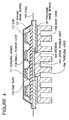
- FIG. 4 there is shown a sectional view of a first embodiment of the multi-chip module semiconductor device in accordance with the present invention.
- a package base board 101 is formed of ceramics, for example, and has a plurality of leads 102 outward projecting from a periphery of the base board 101.
- Tile base board 101 also includes a plurality of wirings (not shown) which are electrically connected to the leads 102 and which are exposed at a plurality of predetermined portions (not shown) in an upper surface of the package base board 101.
- a recess 103 is formed at a portion of the upper surface of the package base board 101, for example, at a center region of the upper surface of the package base board 101, and a through hole 104 is formed within the recess 103 to pass through the package base board 101.
- a large power semiconductor device chip 105 having a large consumed electric power is mounted within the recess 103.
- a heat sink 106 is fixed on a lower surface side of the package base board 101, in such a manner that the heat sink 106 is in direct contact with a lower surface of the large power chip 105 in the through hole 104.
- a wiring base board 107 having a multi-layer wiring structure is put on the package base board 101 assembled with the large power chip 105 as mentioned above, and the wiring base board 107 is fixed to the package base board 101 in such a manner that electrodes (not shown) exposed at a lower surface of the wiring base board 107 are electrically connected by use of an electrically conductive bonding agent (not shown) to the wirings (not shown) exposed at the upper surface of the package base board 101.
- a plurality of semiconductor device chips 108 having a small consumed electric power are mounted on an upper surface of the wiring base board 107.
- a so called TAB tape is used in order to mount the small power chips 108 on the wiring base board 107.
- the small power chips 108 are mechanically and electrically connected onto the wiring base board 107 by a TAB tape 109.
- a cap 110 is mounted to cover the wiring base board 107 and the small power chips 108 in such a manner that a periphery of the cap 110 is bonded to the upper surface of the package base board 101 by a bonding agent (not shown) so that the wiring base board 107 and the small power chips 108 are encapsulated by the cap 110 and the package base board 101.
- the small power chips 108 are bonded to an internal surface of the cap 110 by means of a bonding agent 111 having a high thermal conductivity.
- the heat sink 106 is mounted to the package base board 101 which has the recess 103 and the through hole 104 formed at the center region thereof and the leads 102 projecting from the periphery thereof. Then, the large power chip 105 is mounted on the heat sink 106 exposed within the recess 103 by a bonding agent (not shown) having a high thermal conductivity.
- the wiring base board 107 is put on the package base board 101, and the wiring base board 107 is fixed to die package base board 101 by such a manner that the electrodes (not shown) exposed at the lower surface of the wiring base board 107 are electrically connected by the electrically conductive bonding agent (not shown) to the wirings (not shown) exposed at the upper surface of the package base board 101.
- the wiring base board 107 is previously formed of the multi-layer wiring structure board, but can be formed by sequentially stacking a plurality of thin film wiring circuits.
- a plurality of small power chips 108 connected to the TAB tape 109 are connected onto the wiring base board 107.
- a bonding agent 111 having a high thermal conductivity is put on each of the small power chips 108, and the cap 110 is mounted on the package base board 101 so as to cover the wiring base board 107 and the small power chips 108.
- the small power chips 108 are bonded and thermally coupled to the cap 110 by means of the bonding agent 111.
- heat generated by the large power chip 105 is dissipated through the heat sink 106.
- a portion of the heat is transferred towards the wiring base board 107, but since almost all of the heat is dissipated through the heat sink 106, the heat transferred to the wiring base board 107 is very small.
- heat generated by the plurality of small power chips 108 is transferred through the bonding agent 111 of the high thermal conductivity to the cap 110 and dissipated from the surface of the cap 110. Since these small power chips 108 are mounted on the wiring base board 107 by the TAB tape 109, the chips 108 are not in direct contact with the wiring base board 107, and therefore, only an extremely small portion of the heat generated by each chip 108 is transferred to the wiring base board 107.
- the heat generated by the large power chip 105 scarcely influence the small power chips 108, and the heat generated by the small power chips 108 scarcely influence the large power ship 105. Accordingly, it is no longer necessary to make large the heat sink 106 for the large power chip 105, and therefore, it is possible to scale down the multi-chip module and to increase the integration density of the multi-chip module.
- the bonding agent 111 on the small power chips 108 may be omitted, and the upper surface of the chips 108 can be resiliently contacted with the inner surface of the cap 110 by means of a resilient force of the TAB tapes 109, so that the heat of the chips 108 is directly transferred to the cap 110.
- the bonding agent 111 since the bonding agent 111 is not intervened, a thermal resistance from the chips 108 to the cap 110 is reduced, and therefore, the heat dissipating effect can be elevated.
- FIG. 6 there is shown a sectional view illustrating the multi-chip module shown in Figure 4 mounted on a printed board.
- the leads 102 of the package base board 101 are electrically connected to a printed circuit board 112.
- the cap 110 of the multi-chip module is directed toward the printed circuit board 112 in alignment with a window 113 formed through the printed circuit board 112.
- a heat sink 114 is thermally coupled to the cap 110 through the window 113. With this arrangement, the heat dissipating effect through the cap 110 is enhanced by the heat sink 114.
- a discrete chip 115 are mounted on each of opposite surfaces of the printed circuit board 112.
- FIG. 7 there is shown a sectional view of a second embodiment of the multi-chip module semiconductor device in accordance with the present invention.
- a wiring base board 201 has a plurality of recesses 202 formed on an upper surface thereof separated from each other, and a plurality of small power chips 203 mounted on the upper surface of the board 201 in such a manner that each of the chips 203 is positioned to stride over a corresponding recess 202 and is mechanically and electrically connected to the wiring base board 201 by a flip-chip method which uses bumps 204.
- each chip 203 has a number of electrodes 205 along four side edges of the chip, but the bumps 204 are located along only two side edges opposite to each other, in two arrays in the shown embodiment. Accordingly, the bumps in an outer side array are connected directly to the electrodes positioned thereunder, and the bumps in an inner side array, excluding opposite end bumps of the bump array, are connected through a wiring conductor 206 to a corresponding electrode of the electrodes arranged along each of the remaining two side edges.
- a large power chip 208 is mounted by a thermally insulating material 207, and is mechanically and electrically connected to the wiring base board 201 by use of a TAB tape 209.
- a resin 210 is injected to cover only a periphery of each small power chip 203 where the bumps 204 are provided, and a resin 211 is also injected to cover the TAB tape 209 of the large power chip 208.
- a heat sink and a cap are contacted to the large power chip 208 and the small power chips 203, respectively.
- a heat sink 212 and a heat sink 213 can be contacted to the large power chip 208 and the small power chips 203, respectively.
- heat generated by the small power chips 203 are dissipated through the cap (not shown) or the heat sink 213 in contact with the small power chips 203. Since a space formed between the recess 202 of the wiring base board 201 and the lower surface of the small power chip 203, functions as a thermally insulating air layer, the transfer of the heat generated by the small power chips 203 towards the wiring base board 201 is effectively suppressed by the thermally insulating air layer. In this connection, since the recess 202 communicates with an external space through the gap formed between the wiring base board 201 and the lower surface of the chip 203 at two side edge regions on which the bumps are not located, the heat dissipating effect is enhanced by a flow of air through the gap.
- the thermally insulating material 207 provided for the large power chip 208 can be replaced by a space similar to the space formed in the recess 202 for the small power chip 203, and also, the space formed in the recess 202 for the small power chip 203 can be replaced with a thermally insulating material 207 similar to the thermally insulating material 207 provided for the large power chip 208.
- the thermally insulating material 207 provided for the large power chip 208 can be replaced by a space similar to the space formed in the recess 202 for the small power chip 203, and also, the space formed in the recess 202 for the small power chip 203 can be replaced with a thermally insulating material 207 similar to the thermally insulating material 207 provided for the large power chip 208.
- the thermally insulating structure formed between each surface of the wiring base board and the corresponding chips and therefore, the integrated density of the multi-chip module can be elevated.
- the chip(s) mounted on each one surface of the base board is heat-dissipated through the associated individual heat dissipating member, independent of the heat dissipating member provided for the chip(s) mounted on the other surface of the base board. Therefore, heat generated in the chip(s) mounted on each one surface of the base board will never adversely influence to the chip(s) mounted on the other surface of the base board. Accordingly, it is possible to overcome the problem occurring when the chips are mounted on opposite surfaces of the base board in the prior art, and also it is possible to increase the integration density of the multi-chip module.
- the thermally insulating structure is intervened between each of opposite surfaces of the base board and the chip(s) mounted on the same surface of the base board, heat generated in each chip is prevented from being transferred to the base board. Therefore, heat generated in each chip will never adversely influence to the other chips. Accordingly, it is possible to overcome the problem occurring when the chips are mounted on opposite surfaces of the base board in the prior art, and also it is possible to increase the integration density of the multi-chip module.
Landscapes
- Engineering & Computer Science (AREA)
- Microelectronics & Electronic Packaging (AREA)
- Cooling Or The Like Of Semiconductors Or Solid State Devices (AREA)
Applications Claiming Priority (2)
| Application Number | Priority Date | Filing Date | Title |
|---|---|---|---|
| JP193757/94 | 1994-07-26 | ||
| JP6193757A JP2611671B2 (ja) | 1994-07-26 | 1994-07-26 | 半導体装置 |
Publications (2)
| Publication Number | Publication Date |
|---|---|
| EP0694968A2 true EP0694968A2 (de) | 1996-01-31 |
| EP0694968A3 EP0694968A3 (de) | 1996-09-11 |
Family
ID=16313311
Family Applications (1)
| Application Number | Title | Priority Date | Filing Date |
|---|---|---|---|
| EP95111789A Withdrawn EP0694968A3 (de) | 1994-07-26 | 1995-07-26 | Halbleiter-Multichip-Baustein |
Country Status (3)
| Country | Link |
|---|---|
| EP (1) | EP0694968A3 (de) |
| JP (1) | JP2611671B2 (de) |
| CA (1) | CA2154719A1 (de) |
Cited By (6)
| Publication number | Priority date | Publication date | Assignee | Title |
|---|---|---|---|---|
| EP0996155A3 (de) * | 1998-10-23 | 2001-04-18 | Sony Corporation | Vorrichtung mit integrierter Schaltung für Hochfrequenz |
| EP1271649A3 (de) * | 2001-06-21 | 2004-04-28 | ATI Technologies Inc. | Mehrchip-Modul und zugehörige Methode |
| EP1827065A3 (de) * | 1997-02-03 | 2007-10-10 | Ibiden Co., Ltd. | Leiterplatte und Herstellungsverfahren dafür |
| CN103117275A (zh) * | 2013-01-31 | 2013-05-22 | 华为技术有限公司 | 一种芯片封装结构及芯片封装方法 |
| CN113097162A (zh) * | 2017-10-10 | 2021-07-09 | 北京比特大陆科技有限公司 | 散热片、芯片及电路板 |
| WO2024060786A1 (zh) * | 2022-09-20 | 2024-03-28 | 华为技术有限公司 | 光收发模块及通信设备 |
Families Citing this family (7)
| Publication number | Priority date | Publication date | Assignee | Title |
|---|---|---|---|---|
| KR100351925B1 (ko) * | 2000-10-25 | 2002-09-12 | 앰코 테크놀로지 코리아 주식회사 | 적층형 반도체 패키지 |
| JP5034143B2 (ja) * | 2001-04-27 | 2012-09-26 | パナソニック株式会社 | パワー変換装置 |
| KR100809701B1 (ko) * | 2006-09-05 | 2008-03-06 | 삼성전자주식회사 | 칩간 열전달 차단 스페이서를 포함하는 멀티칩 패키지 |
| JP2011023463A (ja) | 2009-07-14 | 2011-02-03 | Denso Corp | 半導体モジュール |
| JP5898906B2 (ja) * | 2011-10-06 | 2016-04-06 | 新電元工業株式会社 | 半導体素子の電気接続構造 |
| KR102218766B1 (ko) * | 2018-12-10 | 2021-02-22 | 주식회사 코스텍시스 | 반도체 디바이스 패키지 |
| CN119725237A (zh) * | 2023-09-28 | 2025-03-28 | 比亚迪股份有限公司 | 功率模块及具有其的车辆 |
Citations (3)
| Publication number | Priority date | Publication date | Assignee | Title |
|---|---|---|---|---|
| JPS5965457A (ja) | 1982-10-05 | 1984-04-13 | Mitsubishi Electric Corp | 半導体装置 |
| JPS6147653A (ja) | 1984-08-13 | 1986-03-08 | Hitachi Ltd | 半導体装置 |
| JPH05136323A (ja) | 1991-11-13 | 1993-06-01 | Nec Corp | 集積回路装置 |
Family Cites Families (6)
| Publication number | Priority date | Publication date | Assignee | Title |
|---|---|---|---|---|
| US4774632A (en) * | 1987-07-06 | 1988-09-27 | General Electric Company | Hybrid integrated circuit chip package |
| DE4015788C2 (de) * | 1990-05-16 | 1994-06-23 | Siemens Nixdorf Inf Syst | Baugruppe |
| JPH0548000A (ja) * | 1991-08-13 | 1993-02-26 | Fujitsu Ltd | 半導体装置 |
| JPH06125037A (ja) * | 1992-04-07 | 1994-05-06 | Megachitsupusu:Kk | 半導体装置 |
| JPH06188361A (ja) * | 1992-05-11 | 1994-07-08 | Nec Corp | マルチチップモジュール基板 |
| JP3521931B2 (ja) * | 1993-06-02 | 2004-04-26 | セイコーエプソン株式会社 | 半導体装置及びその製造方法 |
-
1994
- 1994-07-26 JP JP6193757A patent/JP2611671B2/ja not_active Expired - Lifetime
-
1995
- 1995-07-26 CA CA002154719A patent/CA2154719A1/en not_active Abandoned
- 1995-07-26 EP EP95111789A patent/EP0694968A3/de not_active Withdrawn
Patent Citations (3)
| Publication number | Priority date | Publication date | Assignee | Title |
|---|---|---|---|---|
| JPS5965457A (ja) | 1982-10-05 | 1984-04-13 | Mitsubishi Electric Corp | 半導体装置 |
| JPS6147653A (ja) | 1984-08-13 | 1986-03-08 | Hitachi Ltd | 半導体装置 |
| JPH05136323A (ja) | 1991-11-13 | 1993-06-01 | Nec Corp | 集積回路装置 |
Cited By (11)
| Publication number | Priority date | Publication date | Assignee | Title |
|---|---|---|---|---|
| EP1827065A3 (de) * | 1997-02-03 | 2007-10-10 | Ibiden Co., Ltd. | Leiterplatte und Herstellungsverfahren dafür |
| US7552531B2 (en) | 1997-02-03 | 2009-06-30 | Ibiden Co., Ltd. | Method of manufacturing a printed wiring board having a previously formed opening hole in an innerlayer conductor circuit |
| EP0996155A3 (de) * | 1998-10-23 | 2001-04-18 | Sony Corporation | Vorrichtung mit integrierter Schaltung für Hochfrequenz |
| EP1271649A3 (de) * | 2001-06-21 | 2004-04-28 | ATI Technologies Inc. | Mehrchip-Modul und zugehörige Methode |
| US7215022B2 (en) | 2001-06-21 | 2007-05-08 | Ati Technologies Inc. | Multi-die module |
| EP2362416A3 (de) * | 2001-06-21 | 2012-03-28 | ATI Technologies Inc. | Multichipmodul und zugehörige Methode |
| CN103117275A (zh) * | 2013-01-31 | 2013-05-22 | 华为技术有限公司 | 一种芯片封装结构及芯片封装方法 |
| CN103117275B (zh) * | 2013-01-31 | 2015-08-19 | 华为技术有限公司 | 一种芯片封装结构及芯片封装方法 |
| US9466597B2 (en) | 2013-01-31 | 2016-10-11 | Huawei Technologies Co., Ltd. | Chip package structure and chip packaging method |
| CN113097162A (zh) * | 2017-10-10 | 2021-07-09 | 北京比特大陆科技有限公司 | 散热片、芯片及电路板 |
| WO2024060786A1 (zh) * | 2022-09-20 | 2024-03-28 | 华为技术有限公司 | 光收发模块及通信设备 |
Also Published As
| Publication number | Publication date |
|---|---|
| JPH0846134A (ja) | 1996-02-16 |
| CA2154719A1 (en) | 1996-01-27 |
| EP0694968A3 (de) | 1996-09-11 |
| JP2611671B2 (ja) | 1997-05-21 |
Similar Documents
| Publication | Publication Date | Title |
|---|---|---|
| US5646831A (en) | Electrically enhanced power quad flat pack arrangement | |
| US6545351B1 (en) | Underside heat slug for ball grid array packages | |
| US6114761A (en) | Thermally-enhanced flip chip IC package with extruded heatspreader | |
| US5598031A (en) | Electrically and thermally enhanced package using a separate silicon substrate | |
| US6303997B1 (en) | Thin, stackable semiconductor packages | |
| US6657296B2 (en) | Semicondctor package | |
| KR100269528B1 (ko) | 고성능 멀티 칩 모듈 패키지 | |
| US5629561A (en) | Semiconductor package with integral heat dissipator | |
| US5067005A (en) | Semiconductor device | |
| US6271581B2 (en) | Semiconductor package structure having universal lead frame and heat sink | |
| US5796159A (en) | Thermally efficient integrated circuit package | |
| US5525835A (en) | Semiconductor chip module having an electrically insulative thermally conductive thermal dissipator directly in contact with the semiconductor element | |
| US5939781A (en) | Thermally enhanced integrated circuit packaging system | |
| CA2154719A1 (en) | Multi-chip module semiconductor device | |
| KR960000222B1 (ko) | 히트-싱크를 갖춘 반도체 패키지 | |
| JPH1056093A (ja) | 半導体装置およびその半導体装置を組み込んだ電子装置 | |
| US6008988A (en) | Integrated circuit package with a heat spreader coupled to a pair of electrical devices | |
| JP7551571B2 (ja) | 半導体モジュール | |
| GB2168533A (en) | Package for integrated circuits having improved heat sinking capabilities | |
| JP3253154B2 (ja) | 半導体装置用パッケージ及び半導体装置 | |
| KR100474193B1 (ko) | 비지에이패키지및그제조방법 | |
| KR100276858B1 (ko) | 향상된패드설계를갖는전자패키지 | |
| JPH09330994A (ja) | 半導体装置 | |
| KR20020039010A (ko) | 방열판을 갖는 이중 칩 패키지 | |
| KR0156513B1 (ko) | 반도체패키지 |
Legal Events
| Date | Code | Title | Description |
|---|---|---|---|
| PUAI | Public reference made under article 153(3) epc to a published international application that has entered the european phase |
Free format text: ORIGINAL CODE: 0009012 |
|
| AK | Designated contracting states |
Kind code of ref document: A2 Designated state(s): DE GB IT |
|
| PUAL | Search report despatched |
Free format text: ORIGINAL CODE: 0009013 |
|
| AK | Designated contracting states |
Kind code of ref document: A3 Designated state(s): DE GB IT |
|
| 17P | Request for examination filed |
Effective date: 19960801 |
|
| 17Q | First examination report despatched |
Effective date: 19970521 |
|
| STAA | Information on the status of an ep patent application or granted ep patent |
Free format text: STATUS: THE APPLICATION HAS BEEN WITHDRAWN |
|
| 18W | Application withdrawn |
Withdrawal date: 19971103 |