EP0694976A2 - Method of manufacturing an integrated circuit having p-MOSFETs with different channel widths - Google Patents
Method of manufacturing an integrated circuit having p-MOSFETs with different channel widths Download PDFInfo
- Publication number
- EP0694976A2 EP0694976A2 EP95480068A EP95480068A EP0694976A2 EP 0694976 A2 EP0694976 A2 EP 0694976A2 EP 95480068 A EP95480068 A EP 95480068A EP 95480068 A EP95480068 A EP 95480068A EP 0694976 A2 EP0694976 A2 EP 0694976A2
- Authority
- EP
- European Patent Office
- Prior art keywords
- fets
- latchup
- sites
- channel
- implant
- Prior art date
- Legal status (The legal status is an assumption and is not a legal conclusion. Google has not performed a legal analysis and makes no representation as to the accuracy of the status listed.)
- Withdrawn
Links
Images


Classifications
-
- H—ELECTRICITY
- H10—SEMICONDUCTOR DEVICES; ELECTRIC SOLID-STATE DEVICES NOT OTHERWISE PROVIDED FOR
- H10D—INORGANIC ELECTRIC SEMICONDUCTOR DEVICES
- H10D62/00—Semiconductor bodies, or regions thereof, of devices having potential barriers
- H10D62/10—Shapes, relative sizes or dispositions of the regions of the semiconductor bodies; Shapes of the semiconductor bodies
- H10D62/17—Semiconductor regions connected to electrodes not carrying current to be rectified, amplified or switched, e.g. channel regions
- H10D62/393—Body regions of DMOS transistors or IGBTs
-
- H—ELECTRICITY
- H10—SEMICONDUCTOR DEVICES; ELECTRIC SOLID-STATE DEVICES NOT OTHERWISE PROVIDED FOR
- H10D—INORGANIC ELECTRIC SEMICONDUCTOR DEVICES
- H10D30/00—Field-effect transistors [FET]
- H10D30/60—Insulated-gate field-effect transistors [IGFET]
- H10D30/637—Lateral IGFETs having no inversion channels, e.g. buried channel lateral IGFETs, normally-on lateral IGFETs or depletion-mode lateral IGFETs
-
- H—ELECTRICITY
- H10—SEMICONDUCTOR DEVICES; ELECTRIC SOLID-STATE DEVICES NOT OTHERWISE PROVIDED FOR
- H10D—INORGANIC ELECTRIC SEMICONDUCTOR DEVICES
- H10D62/00—Semiconductor bodies, or regions thereof, of devices having potential barriers
- H10D62/10—Shapes, relative sizes or dispositions of the regions of the semiconductor bodies; Shapes of the semiconductor bodies
- H10D62/113—Isolations within a component, i.e. internal isolations
-
- H—ELECTRICITY
- H10—SEMICONDUCTOR DEVICES; ELECTRIC SOLID-STATE DEVICES NOT OTHERWISE PROVIDED FOR
- H10D—INORGANIC ELECTRIC SEMICONDUCTOR DEVICES
- H10D62/00—Semiconductor bodies, or regions thereof, of devices having potential barriers
- H10D62/10—Shapes, relative sizes or dispositions of the regions of the semiconductor bodies; Shapes of the semiconductor bodies
- H10D62/17—Semiconductor regions connected to electrodes not carrying current to be rectified, amplified or switched, e.g. channel regions
- H10D62/213—Channel regions of field-effect devices
- H10D62/221—Channel regions of field-effect devices of FETs
- H10D62/235—Channel regions of field-effect devices of FETs of IGFETs
-
- H—ELECTRICITY
- H10—SEMICONDUCTOR DEVICES; ELECTRIC SOLID-STATE DEVICES NOT OTHERWISE PROVIDED FOR
- H10D—INORGANIC ELECTRIC SEMICONDUCTOR DEVICES
- H10D84/00—Integrated devices formed in or on semiconductor substrates that comprise only semiconducting layers, e.g. on Si wafers or on GaAs-on-Si wafers
- H10D84/80—Integrated devices formed in or on semiconductor substrates that comprise only semiconducting layers, e.g. on Si wafers or on GaAs-on-Si wafers characterised by the integration of at least one component covered by groups H10D12/00 or H10D30/00, e.g. integration of IGFETs
- H10D84/82—Integrated devices formed in or on semiconductor substrates that comprise only semiconducting layers, e.g. on Si wafers or on GaAs-on-Si wafers characterised by the integration of at least one component covered by groups H10D12/00 or H10D30/00, e.g. integration of IGFETs of only field-effect components
- H10D84/83—Integrated devices formed in or on semiconductor substrates that comprise only semiconducting layers, e.g. on Si wafers or on GaAs-on-Si wafers characterised by the integration of at least one component covered by groups H10D12/00 or H10D30/00, e.g. integration of IGFETs of only field-effect components of only insulated-gate FETs [IGFET]
- H10D84/85—Complementary IGFETs, e.g. CMOS
- H10D84/854—Complementary IGFETs, e.g. CMOS comprising arrangements for preventing bipolar actions between the different IGFET regions, e.g. arrangements for latchup prevention
Definitions
- the field of the invention in that of buried channel p-FET integrated circuit processing in which the transistors are isolated by trenches and in which the groundrules are in the range of about 0.25 ⁇ m.
- corner conduction in trench isolated n-MOSFETs may be a significant contributor to standby current in low standby power ULSI applications, as described in A. Bryant, et al "The current-carrying corner inherent to trench isolation", IEEE Electron Device Letters, vol 14, no. 8, pp. 412-414, 1993 and B. Davari, et al "A variable-size shallow trench isolation (STI) technology with diffused sidewall doping for submicron CMOS", 1988 IEDM Technical Digest, pp. 92-95, 1988.
- the invention relates to a CMOS integrated circuit in which a performance advantage for p-FETS is achieved by use of an anomalous narrow channel effect.
- a feature of the invention is the use of wide transistors having a V t chosen to meet off-current design objectives together with narrow transistors having a reduced V t for improved performance.
- Another feature of the invention is the use of improved performance high-current transistors comprising a number of narrow transistors connected in parallel.
- Figure 1 illustrates measured and predicted values of V t for different buried-channel transistor widths.
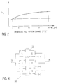
- Figure 2 illustrates the dependence of V t on channel width for buried-channel p-FET having channel widths in the range of 2 -20 ⁇ m.
- Figure 3 illustrates the distribution of Boron concentration in a buried-channel p-FET.
- Figure 4 illustrates a high-current low V t transistor set.
- Fig. 2 illustrates the relationship for a wider range of channel width. If the buried-channel boron dose is decreased to assure that the off current is less than or equal to the design objective off current over the entire range of design widths, as would be consistent with the prior art, the performance of the widest devices is compromised as a result of higher than desired V t . A loss of overdrive of 100mv on the widest devices is typical.
- a performance advantage based on the anomalous narrow channel effect can be realized by using relatively narrow (2 -10 ⁇ m) devices for the logic circuitry and wide (> 20 ⁇ m) devices for the inverters that drive large loads by setting the V t of the widest devices to meet the off-current objective, which permits a reduction in the magnitude of V t for the narrower devices, thus giving improved performance.
- the V t for the devices is initially set by the buried channel implant, conventionally done after the deep (or latchup) implant. The deep implant then raises V t for the wider devices. Since most of the standby current is contributed by the wide devices, this approach has little effect on total standby current.
- the anomalous narrow channel effect results from a "boron puddle” or localized increase in the boron concentration near the edge of the isolation trenches created by transient enhanced diffusion (TED) of the boron in the buried layer.
- TED transient enhanced diffusion
- the TED results from an excess interstitial (described in "Paint Defects and Diffusion in Silicon", P. M. Fahey, et al Reviews of Modern Physics, vol 61, no. 2, April 1989) distribution arising from damage caused by the 2.5x10¹³/cm2, 500 keV phosphorous implant used for latchup suppression, in conjunction with strong excess interstitial recombination on the top surface and trench sidewalls of the device.
- the anomalous narrow channel effect can be enhanced by increasing the implanted point defect concentration. These point defects provide the source of the excess interstitials that drive the formation of the boron puddle and therefore the anomalous narrow channel effect.
- the term “latchup dose” will be taken to mean an implant of 2.5x10¹³/cm2 at an energy of 500keV and the term “latchup-threshold dose” will be taken to mean a dose greater than 4x10¹³/cm at an energy of greater than 500keV. Also, the terms “narrow” and “wide” when applied to the p-FET channel width will be taken to mean less than about 10 ⁇ m and greater than about 10 ⁇ m, respectively.
- the energy of the deep implant can be increased (illustratively to 1MeV) for even greater enhancement by increasing the crystal damage caused by the implant. Additionally, the use of higher implant energies moves the tail far enough from the surface that even greater doses can be used without affecting the device doping. Implanting other species such as silicon or any other species that is not electrically active can also be used to increase the anomalous narrow channel effect without affecting the latchup effect of the deep implant.
- the addition of an annealing step between the deep implantation and the gate oxidation of 60 minutes at 800°C provides for rapid excess interstitial recombination on the Si/SiO2 interfaces, which greatly reduces the TED of boron during the 850°C gate oxidation.
- the gate oxide (illustratively about 10nm) may be formed at a higher temperature such as 1050°C for a correspondingly shorter time that reduces the TED.
- the boron diffusivity at the depth of maximum boron concentration increases and the boron distribution broadens from trench edge toward the middle of the area between the trenches (the active area).
- the minimum in the peak net p-type concentration of the buried layer occurs at mid-width and is accentuated by the compensation of boron by the n-well doping.
- the gradient in the excess interstitial concentration drives the boron towards the trench edge.
- segregation induced boron depletion and n-type dopant pile-up reduce the net p-type concentration.
- Modeling shows that the peak net p-type concentration in the "boron puddle" is approximately 32% greater than at mid-width, for a 2 ⁇ m wide device. As the device width is reduced down to approximately 0.4 ⁇ m, the peak net p-type concentration increases because of decreased interstitial concentration at the top surface resulting from recombination on the trench sidewall. For still narrower devices the effect of the n-type dopant pileup on the trench sidewall reduces the buried layer concentration.
- Figure 3 shows measured V t vs W characteristics compared with simulated results obtained from TSUPREM-4 and FIELDAY. It is noteworthy that evidence of a comparable boron puddle for the complementary n-MOSFET is neither observed experimentally, nor predicted by modeling. The use of the extra anneal results in a drastically reduced "boron puddle” and also results in a lower magnitude of wide device V t , since reduced TED of boron leaves a higher peak net p-type concentration in the buried layer.
- Fig 4 illustrates in partially schematic, partially pictorial form a set of transistors denoted generally with the numeral 100 having a source node 30, a drain node 40 and a common gate 20.
- Each of the N transistors in the set 10-1 to 10-N has a channel width Wn chosen to provide the desired V t .
- the total number N is chosen to provide the required current for the application in question.
- the phrase “preparing the substrate” will be used to indicate conventional steps such as growing an epitaxial layer (where used), performing a threshold implant, cutting and filling trenches for isolation, forming p-and n- wells etc.
- the phrase “completing the circuit” will be used to indicate the remaining steps after the deep implant such as completing the transistors p-FET and/or n-FETs and forming the interconnections, etc.
Landscapes
- Metal-Oxide And Bipolar Metal-Oxide Semiconductor Integrated Circuits (AREA)
- Element Separation (AREA)
- Insulated Gate Type Field-Effect Transistor (AREA)
Abstract
Description
- The field of the invention in that of buried channel p-FET integrated circuit processing in which the transistors are isolated by trenches and in which the groundrules are in the range of about 0.25µm.
- It has been known that corner conduction in trench isolated n-MOSFETs may be a significant contributor to standby current in low standby power ULSI applications, as described in A. Bryant, et al "The current-carrying corner inherent to trench isolation", IEEE Electron Device Letters, vol 14, no. 8, pp. 412-414, 1993 and B. Davari, et al "A variable-size shallow trench isolation (STI) technology with diffused sidewall doping for submicron CMOS", 1988 IEDM Technical Digest, pp. 92-95, 1988. A manifestation of corner conduction is inverse narrow channel effect when the standard current definition of Vt (IVt = 40x(Wdes/Ldes)nA) is applied. However, corner conduction in buried-channel p-MOSFETs has not, heretofore, been recognized as a concern. In buried-channel p-MOSFETs, the polarity of the work function difference between the N+ poly gate and the buried p-layer depletes the buried layer of carriers at low gate voltages. Due to the geometrically enhanced field at the silicon corner, it is expected that, when the doping is uniform across the device width, the magnitude of Vt at the corners of these devices is greater than at mid-channel. This leads to a normal narrow channel effect.
- The invention relates to a CMOS integrated circuit in which a performance advantage for p-FETS is achieved by use of an anomalous narrow channel effect.
- A feature of the invention is the use of wide transistors having a Vt chosen to meet off-current design objectives together with narrow transistors having a reduced Vt for improved performance.
- Another feature of the invention is the use of improved performance high-current transistors comprising a number of narrow transistors connected in parallel.
- Figure 1 illustrates measured and predicted values of Vt for different buried-channel transistor widths.
- Figure 2 illustrates the dependence of Vt on channel width for buried-channel p-FET having channel widths in the range of 2 -20µm.
- Figure 3 illustrates the distribution of Boron concentration in a buried-channel p-FET.
- Figure 4 illustrates a high-current low Vt transistor set.
- An anomalous narrow channel behavior has been observed on buried-channel p-MOSFETs based on a 0.25 µm CMOS process. The magnitude of the threshold voltage decreases when going from very wide devices to approximately 0.4 µm width (referred to as the inverse narrow channel effect). For devices narrower than 0.4 µm, the expected normal narrow channel effect is observed' as described in K. Ohe, et al "Narrow-width effects of shallow trench-isolated CMOS with n⁺ polysilicon gate!, IEEE Trans. Electron Devices, vol. 36, no. 6, pp. 1110-1116, 1989. Fig 1 shows the relationship between Vt and channel width for buried-channel p-FETs having gate oxide thickness of about 10nm and VDS of 0.1V. These characteristics are also typical of transistors of shorter channel length and higher drain-source voltage.
- Fig. 2 illustrates the relationship for a wider range of channel width. If the buried-channel boron dose is decreased to assure that the off current is less than or equal to the design objective off current over the entire range of design widths, as would be consistent with the prior art, the performance of the widest devices is compromised as a result of higher than desired Vt. A loss of overdrive of 100mv on the widest devices is typical.
- A performance advantage based on the anomalous narrow channel effect can be realized by using relatively narrow (2 -10µm) devices for the logic circuitry and wide (> 20µm) devices for the inverters that drive large loads by setting the Vt of the widest devices to meet the off-current objective, which permits a reduction in the magnitude of Vt for the narrower devices, thus giving improved performance. As is known, the Vt for the devices is initially set by the buried channel implant, conventionally done after the deep (or latchup) implant. The deep implant then raises Vt for the wider devices. Since most of the standby current is contributed by the wide devices, this approach has little effect on total standby current.
- It has been found that the anomalous narrow channel effect results from a "boron puddle" or localized increase in the boron concentration near the edge of the isolation trenches created by transient enhanced diffusion (TED) of the boron in the buried layer. The TED, in turn, results from an excess interstitial (described in "Paint Defects and Diffusion in Silicon", P. M. Fahey, et al Reviews of Modern Physics, vol 61, no. 2, April 1989) distribution arising from damage caused by the 2.5x10¹³/cm2, 500 keV phosphorous implant used for latchup suppression, in conjunction with strong excess interstitial recombination on the top surface and trench sidewalls of the device.
- The performance improvement due to the anomalous narrow channel effect has been modelled using SPICE and it has been found that, for a typical delta Vt of 100mV between devices having p-channel width Wp of Wp = 2µm and Wp = 20µm, there is a performance improvement of 4.7% using NAND logic. If the delta Vt is increased to 200mV by enhancing the anomalous narrow channel effect, the performance improvement increases to 9.3%. Even greater performance improvements can be obtained using NOR logic, without any increase in standby current.
- The anomalous narrow channel effect can be enhanced by increasing the implanted point defect concentration. These point defects provide the source of the excess interstitials that drive the formation of the boron puddle and therefore the anomalous narrow channel effect. One method of enhancement is that of increasing the dose of the deep phosphorous implant. Such an increase does not have an effect on device operation because the dopant provided by this implant is too deep ( ∼ 0.8µm) to affect the device. Indeed, the increase in dopant also improves latchup suppression. Doubling the deep implant dose at the same energy is shown in simulations to increase the delta Vt (between Wp = 2 to 20µm) from 100mV to 200mV.
- For purposes of the claims, the term "latchup dose" will be taken to mean an implant of 2.5x10¹³/cm2 at an energy of 500keV and the term "latchup-threshold dose" will be taken to mean a dose greater than 4x10¹³/cm at an energy of greater than 500keV. Also, the terms "narrow" and "wide" when applied to the p-FET channel width will be taken to mean less than about 10µm and greater than about 10µm, respectively.
- In addition, the energy of the deep implant can be increased (illustratively to 1MeV) for even greater enhancement by increasing the crystal damage caused by the implant. Additionally, the use of higher implant energies moves the tail far enough from the surface that even greater doses can be used without affecting the device doping. Implanting other species such as silicon or any other species that is not electrically active can also be used to increase the anomalous narrow channel effect without affecting the latchup effect of the deep implant.
- If, on the other hand, it is desired to reduce the anomalous narrow channel effect, the addition of an annealing step between the deep implantation and the gate oxidation of 60 minutes at 800°C provides for rapid excess interstitial recombination on the Si/SiO2 interfaces, which greatly reduces the TED of boron during the 850°C gate oxidation. Alternatively, the gate oxide (illustratively about 10nm) may be formed at a higher temperature such as 1050°C for a correspondingly shorter time that reduces the TED.
- In a conventional process, a 15 minute, 850°C dry gate oxidation immediately follows the n-well and boron buried-channel implants. An 800°C 60 minute anneal immediately following the deep phosphorus implant and prior to the gate oxidation results in rapid excess interstitial recombination on the Si/SiO2 interfaces. Thus, TED of boron is greatly reduced during the subsequent 850°C gate oxidation. Measurements and simulation confirm that the "boron puddle" and anomalous narrow channel effect are greatly reduced (net p-type concentration peaks only 3% above mid-width value for a device width of 2µm). The boron diffusivity at the depth of maximum boron concentration (∼ 30nm) increases and the boron distribution broadens from trench edge toward the middle of the area between the trenches ( the active area). The minimum in the peak net p-type concentration of the buried layer occurs at mid-width and is accentuated by the compensation of boron by the n-well doping. Furthermore, the gradient in the excess interstitial concentration drives the boron towards the trench edge. Within approximately 30 nm of the trench edge, segregation induced boron depletion and n-type dopant pile-up reduce the net p-type concentration.
- The overall effect of the excess interstitial distribution on the diffusion of boron during the 850°C gate oxidation is the creation of a "boron puddle" near the trench edge, as shown by the simulated net doping distribution at end of process in Figure 3 for a channel width of about 0.9µm.
- Modeling shows that the peak net p-type concentration in the "boron puddle" is approximately 32% greater than at mid-width, for a 2 µm wide device. As the device width is reduced down to approximately 0.4 µm, the peak net p-type concentration increases because of decreased interstitial concentration at the top surface resulting from recombination on the trench sidewall. For still narrower devices the effect of the n-type dopant pileup on the trench sidewall reduces the buried layer concentration. Figure 3 shows measured Vt vs W characteristics compared with simulated results obtained from TSUPREM-4 and FIELDAY. It is noteworthy that evidence of a comparable boron puddle for the complementary n-MOSFET is neither observed experimentally, nor predicted by modeling. The use of the extra anneal results in a drastically reduced "boron puddle" and also results in a lower magnitude of wide device Vt, since reduced TED of boron leaves a higher peak net p-type concentration in the buried layer.
- In addition to setting the deep implant parameters to provide low leakage for wide devices and enhance performance for logic devices, it is also possible to take advantage of the dependence of Vt on width to provide for low Vt where it is needed for high-current applications by connecting a number of narrow channel devices in parallel to provide the desired total current. Fig 4 illustrates in partially schematic, partially pictorial form a set of transistors denoted generally with the numeral 100 having a
source node 30, adrain node 40 and acommon gate 20. Each of the N transistors in the set 10-1 to 10-N has a channel width Wn chosen to provide the desired Vt. The total number N is chosen to provide the required current for the application in question. - Those skilled in the art are well aware that there are many steps in an integrated circuit process. For convenience in terminology, the phrase "preparing the substrate" will be used to indicate conventional steps such as growing an epitaxial layer (where used), performing a threshold implant, cutting and filling trenches for isolation, forming p-and n- wells etc. Similarly, the phrase "completing the circuit" will be used to indicate the remaining steps after the deep implant such as completing the transistors p-FET and/or n-FETs and forming the interconnections, etc.
Claims (7)
- A method of forming an integrated circuit having buried channel p-FETs isolated by trench isolation comprising the steps of:
preparing the substrate;
performing a deep implant in p-sites below the sites of p-FETs to suppress latchup in p-FETs, said deep implant having a latchup dose and latchup energy;
forming p-FETs above said p-sites including performing a buried channel implant to set a logic Vt; and
completing said circuit, characterized in that:
said deep implant is set to provide a delta Vt for a p-FET having a channel width greater than 10 µm relative to said logic Vt set by said buried channel implant for narrow p-FETs, whereby p-FETs in the circuit have different Vt dependent on the channel width of the p-FET. - A method according to claim 1, further characterized in that said latchup concentration is greater than 2.5x10¹³/cm.
- A method according to claim 1, further characterized in that said latchup energy is greater than 500 keV.
- A method according to claim 2, further characterized in that said latchup energy is greater than 500 keV.
- A method of forming an integrated circuit having buried channel p-FETs isolated by trench isolation comprising the steps of:
preparing the substrate;
performing a deep implant in p-sites below the sites of p-FETs to suppress latchup in p-FETs, said deep implant having a latchup concentration and latchup energy;
forming p-FETs above said p-sites; and
completing said circuit, characterized in that:
said step of performing a deep implant is followed by a step of annealing crystal damage before a step of gate oxidation, whereby TED is reduced and Vt of p-FETs having various channel widths is made more uniform. - A method of forming an integrated circuit having buried channel p-FETs isolated by trench isolation comprising the steps of:
preparing the substrate;
performing a deep implant in p-sites below the sites of p-FETs to suppress latchup in p-FETs, said deep implant having a latchup concentration and latchup energy;
forming p-FETs above said p-sites; and
completing said circuit, characterized in that:
said step of performing a deep implant is followed by a step of gate oxidation at a temperature greater than 1,000°C, whereby TED is reduced and Vt of p-FETs having various channel widths is made more uniform. - A method of forming an integrated circuit having buried channel p-FETs isolated by trench isolation comprising the steps of:
preparing the substrate;
performing a deep implant in p-sites below the sites of p-FETs to suppress latchup in p-FETs, said deep implant having a latchup concentration and latchup energy;
forming p-FETs above said p-sites; and
completing said circuit, characterized in that:
said deep implant is set to provide a first Vt for a p-FET having a channel width greater than 10 µm, thereby providing a logic Vt less than said first Vt for narrow p-FETs, whereby p-FETs in the circuit have different Vt dependent on the channel width of the p-FET; and
selected sets of transistors connected in parallel and having a common channel width set to produce a set Vt less than said first Vt, whereby said set of transistors passes high current and also has a Vt less than said first Vt.
Applications Claiming Priority (2)
| Application Number | Priority Date | Filing Date | Title |
|---|---|---|---|
| US269857 | 1994-06-30 | ||
| US08/269,857 US5559050A (en) | 1994-06-30 | 1994-06-30 | P-MOSFETS with enhanced anomalous narrow channel effect |
Publications (2)
| Publication Number | Publication Date |
|---|---|
| EP0694976A2 true EP0694976A2 (en) | 1996-01-31 |
| EP0694976A3 EP0694976A3 (en) | 1996-05-22 |
Family
ID=23028939
Family Applications (1)
| Application Number | Title | Priority Date | Filing Date |
|---|---|---|---|
| EP95480068A Withdrawn EP0694976A3 (en) | 1994-06-30 | 1995-06-09 | Method of manufacturing an integrated circuit comprising p-channel MOSFETs having different channel widths |
Country Status (3)
| Country | Link |
|---|---|
| US (1) | US5559050A (en) |
| EP (1) | EP0694976A3 (en) |
| JP (1) | JPH0846199A (en) |
Cited By (3)
| Publication number | Priority date | Publication date | Assignee | Title |
|---|---|---|---|---|
| EP0720218A3 (en) * | 1994-12-08 | 1998-12-16 | Siemens Aktiengesellschaft | Methods for reducing anomalous narrow channel effect in trench-bounded buried-channel p-MOSFETS |
| EP0889517A1 (en) * | 1997-06-30 | 1999-01-07 | Siemens Aktiengesellschaft | CMOS Integrated circuits with reduced substrate defects |
| US6611680B2 (en) | 1997-02-05 | 2003-08-26 | Telefonaktiebolaget Lm Ericsson (Publ) | Radio architecture |
Families Citing this family (12)
| Publication number | Priority date | Publication date | Assignee | Title |
|---|---|---|---|---|
| US6271093B1 (en) * | 1994-06-30 | 2001-08-07 | Siemens Aktiengesellschaft | Methods for reducing anomalous narrow channel effect in trench-bounded buried-channel p-MOSFETs |
| JP3313024B2 (en) * | 1996-05-27 | 2002-08-12 | 三菱電機株式会社 | Optimization method of trench isolation structure |
| CN1126150C (en) | 1996-06-24 | 2003-10-29 | 松下电器产业株式会社 | Method for manufacturing semiconductor device |
| KR19980055023A (en) * | 1996-12-27 | 1998-09-25 | 김광호 | Most transistor with trench in field area |
| US6069048A (en) * | 1998-09-30 | 2000-05-30 | Lsi Logic Corporation | Reduction of silicon defect induced failures as a result of implants in CMOS and other integrated circuits |
| US6121091A (en) * | 1999-01-19 | 2000-09-19 | Taiwan Semiconductor Manufacturing Company | Reduction of a hot carrier effect phenomena via use of transient enhanced diffusion processes |
| US6117737A (en) * | 1999-02-08 | 2000-09-12 | Taiwan Semiconductor Manufacturing Company | Reduction of a hot carrier effect by an additional furnace anneal increasing transient enhanced diffusion for devices comprised with low temperature spacers |
| US6337260B1 (en) | 1999-09-24 | 2002-01-08 | Advanced Micro Devices, Inc. | Use of knocked-on oxygen atoms for reduction of transient enhanced diffusion |
| JP2001185721A (en) | 1999-12-22 | 2001-07-06 | Nec Corp | Semiconductor device |
| FR2840887B1 (en) | 2002-06-17 | 2004-08-27 | Srct Ind | LOCKING DEVICE FOR CONTAINER HATCH (S) |
| US7200825B2 (en) | 2004-08-27 | 2007-04-03 | International Business Machines Corporation | Methodology of quantification of transmission probability for minority carrier collection in a semiconductor chip |
| JP2009182161A (en) * | 2008-01-31 | 2009-08-13 | Renesas Technology Corp | Semiconductor device |
Family Cites Families (11)
| Publication number | Priority date | Publication date | Assignee | Title |
|---|---|---|---|---|
| US4596068A (en) * | 1983-12-28 | 1986-06-24 | Harris Corporation | Process for minimizing boron depletion in N-channel FET at the silicon-silicon oxide interface |
| JPS60258958A (en) * | 1984-06-06 | 1985-12-20 | Hitachi Ltd | Charge transfer solid-state image sensor |
| JPS62239567A (en) * | 1986-04-11 | 1987-10-20 | Nec Corp | Semiconductor device and its manufacturing method |
| JP2666403B2 (en) * | 1988-01-06 | 1997-10-22 | セイコーエプソン株式会社 | Method of manufacturing MIS type semiconductor device |
| KR940003218B1 (en) * | 1988-03-24 | 1994-04-16 | 세이꼬 엡슨 가부시끼가이샤 | Semiconductor device and manufacturing method thereof |
| JPH02275645A (en) * | 1989-04-17 | 1990-11-09 | Nec Corp | Charge coupled device |
| US5073512A (en) * | 1989-04-21 | 1991-12-17 | Nec Corporation | Method of manufacturing insulated gate field effect transistor having a high impurity density region beneath the channel region |
| JPH04239760A (en) * | 1991-01-22 | 1992-08-27 | Sharp Corp | Manufacture of semiconductor device |
| EP0562207B1 (en) * | 1992-03-27 | 1996-06-05 | International Business Machines Corporation | Method of forming thin film pseudo-planar PFET devices and structures resulting therefrom |
| JP3435173B2 (en) * | 1992-07-10 | 2003-08-11 | 株式会社日立製作所 | Semiconductor device |
| US5395773A (en) * | 1994-03-31 | 1995-03-07 | Vlsi Technology, Inc. | MOSFET with gate-penetrating halo implant |
-
1994
- 1994-06-30 US US08/269,857 patent/US5559050A/en not_active Expired - Lifetime
-
1995
- 1995-06-09 EP EP95480068A patent/EP0694976A3/en not_active Withdrawn
- 1995-06-29 JP JP7164057A patent/JPH0846199A/en active Pending
Non-Patent Citations (3)
| Title |
|---|
| A. BRYANT, ET AL.: "The current-carrying corner inherent to trench isolation", IEEE ELECTRON DEVICE LETTERS, vol. 14, no. 8, 1993, pages 412 - 414, XP011409856, DOI: doi:10.1109/55.225596 |
| B. DAVARI, ET AL.: "A variable-size shallow trench isolation (STI) technology with diffused sidewall doping for submicron CMOS", IEDM TECHNICAL DIGEST, 1988, pages 92 - 95 |
| K. OHE, ET AL.: "Narrow-width effects of shallow trench-isolated CMOS with n+ polysilicon gate", IEEE TRANS. ELECTRON DEVICES, vol. 36, no. 6, 1989, pages 1110 - 1116, XP000003453, DOI: doi:10.1109/16.24355 |
Cited By (5)
| Publication number | Priority date | Publication date | Assignee | Title |
|---|---|---|---|---|
| EP0720218A3 (en) * | 1994-12-08 | 1998-12-16 | Siemens Aktiengesellschaft | Methods for reducing anomalous narrow channel effect in trench-bounded buried-channel p-MOSFETS |
| US6611680B2 (en) | 1997-02-05 | 2003-08-26 | Telefonaktiebolaget Lm Ericsson (Publ) | Radio architecture |
| US6973290B2 (en) | 1997-02-05 | 2005-12-06 | Telefonaktiebolaget L M Ericsson (Publ) | Radio architecture |
| EP0889517A1 (en) * | 1997-06-30 | 1999-01-07 | Siemens Aktiengesellschaft | CMOS Integrated circuits with reduced substrate defects |
| US5937288A (en) * | 1997-06-30 | 1999-08-10 | Siemens Aktiengesellschaft | CMOS integrated circuits with reduced substrate defects |
Also Published As
| Publication number | Publication date |
|---|---|
| US5559050A (en) | 1996-09-24 |
| EP0694976A3 (en) | 1996-05-22 |
| JPH0846199A (en) | 1996-02-16 |
Similar Documents
| Publication | Publication Date | Title |
|---|---|---|
| EP0661751B1 (en) | Method of making a CMOS device with high and low voltage transistors | |
| US5792679A (en) | Method for forming silicon-germanium/Si/silicon dioxide heterostructure using germanium implant | |
| US5559050A (en) | P-MOSFETS with enhanced anomalous narrow channel effect | |
| US4306916A (en) | CMOS P-Well selective implant method | |
| US5427964A (en) | Insulated gate field effect transistor and method for fabricating | |
| EP1225622B1 (en) | Semiconductor device | |
| US20030173591A1 (en) | Radiation-hardened silicon-on-insulator CMOS device, and method of making the same | |
| US10217838B2 (en) | Semiconductor structure with multiple transistors having various threshold voltages | |
| EP0357346B1 (en) | CMOS integrated circuit having improved isolation | |
| US5614433A (en) | Method of fabricating low leakage SOI integrated circuits | |
| WO1985001391A1 (en) | Latch-up immune, multiple retrograde well high density cmos fet | |
| US4701775A (en) | Buried n- channel implant for NMOS transistors | |
| US6103561A (en) | Depletion mode MOS capacitor with patterned VT implants | |
| HK1004351B (en) | Cmos integrated circuit having improved isolation | |
| US6268250B1 (en) | Efficient fabrication process for dual well type structures | |
| US5073509A (en) | Blanket CMOS channel-stop implant | |
| US4568957A (en) | GaAs Complementary enhancement mode junction field effect transistor structures and method of fabrication | |
| US5858826A (en) | Method of making a blanket N-well structure for SRAM data stability in P-type substrates | |
| US6271093B1 (en) | Methods for reducing anomalous narrow channel effect in trench-bounded buried-channel p-MOSFETs | |
| US4679298A (en) | Method of fabrication of GaAs complementary enhancement mode junction field effect transistor | |
| JP2546693B2 (en) | Field effect transistor structure | |
| Mandelman et al. | Anomalous narrow channel effect in trench-isolated buried-channel p-MOSFET's | |
| US20050006703A1 (en) | Radiation-hardened silicon-on-insulator CMOS device, and method of making the same | |
| Pfiester et al. | Improved CMOS field isolation using germanium/boron implantation | |
| EP0720218A2 (en) | Methods for reducing anomalous narrow channel effect in trench-bounded buried-channel p-MOSFETS |
Legal Events
| Date | Code | Title | Description |
|---|---|---|---|
| PUAI | Public reference made under article 153(3) epc to a published international application that has entered the european phase |
Free format text: ORIGINAL CODE: 0009012 |
|
| AK | Designated contracting states |
Kind code of ref document: A2 Designated state(s): AT DE FR GB IE IT NL |
|
| PUAL | Search report despatched |
Free format text: ORIGINAL CODE: 0009013 |
|
| RHK1 | Main classification (correction) |
Ipc: H01L 29/10 |
|
| AK | Designated contracting states |
Kind code of ref document: A3 Designated state(s): AT DE FR GB IE IT NL |
|
| 17P | Request for examination filed |
Effective date: 19960424 |
|
| STAA | Information on the status of an ep patent application or granted ep patent |
Free format text: STATUS: THE APPLICATION HAS BEEN WITHDRAWN |
|
| 18W | Application withdrawn |
Withdrawal date: 19970428 |