EP0696061A2 - Herstellungsverfahren für einen Kontakt in einer integrierten Schaltung - Google Patents
Herstellungsverfahren für einen Kontakt in einer integrierten Schaltung Download PDFInfo
- Publication number
- EP0696061A2 EP0696061A2 EP95304825A EP95304825A EP0696061A2 EP 0696061 A2 EP0696061 A2 EP 0696061A2 EP 95304825 A EP95304825 A EP 95304825A EP 95304825 A EP95304825 A EP 95304825A EP 0696061 A2 EP0696061 A2 EP 0696061A2
- Authority
- EP
- European Patent Office
- Prior art keywords
- layer
- conductive structure
- opening
- forming
- over
- Prior art date
- Legal status (The legal status is an assumption and is not a legal conclusion. Google has not performed a legal analysis and makes no representation as to the accuracy of the status listed.)
- Granted
Links
Images


Classifications
-
- H—ELECTRICITY
- H10—SEMICONDUCTOR DEVICES; ELECTRIC SOLID-STATE DEVICES NOT OTHERWISE PROVIDED FOR
- H10W—GENERIC PACKAGES, INTERCONNECTIONS, CONNECTORS OR OTHER CONSTRUCTIONAL DETAILS OF DEVICES COVERED BY CLASS H10
- H10W20/00—Interconnections in chips, wafers or substrates
- H10W20/01—Manufacture or treatment
- H10W20/071—Manufacture or treatment of dielectric parts thereof
- H10W20/081—Manufacture or treatment of dielectric parts thereof by forming openings in the dielectric parts
Definitions
- the present invention relates generally to semiconductor integrated circuit processing, and more specifically to an improved method of forming a contact in an integrated circuit.
- Enclosure requirements are not consistent with the continued shrinkage of devices. Enclosure is not related to device functionality, but is due primarily to limitations in photolithography alignment capability and is used to insure that misalignment errors do not cause problems with the device. When designing devices having minimum feature and device sizes, minimizing enclosure requirements can significantly impact the overall device size.
- Self-alignment techniques are generally known in the art, and it is known that their use helps minimize enclosure requirements. However, the use of self-alignment techniques has been somewhat limited by device designs in current use.
- MOS FET devices are typically comprised of a gate electrode overlying a channel region and separated therefrom by a gate oxide. Conductive regions are formed in the substrate on either side of the gate electrode and the associated channel to form the source and drain regions.
- the majority of the area required for the source and drain regions is a function of the design layout and the photolithographic steps required, for example, to align the various contact masks and the alignment tolerances.
- an MOS transistor is fabricated by first forming the gate electrode and then the source and drain regions, followed by depositing a layer of interlevel oxide over the substrate. Contact holes are then patterned and cut through the interlevel oxide to expose the underlying source and drain regions. A separate mask is required to pattern the contact holes. This separate mask step further requires an alignment step whereby the mask is aligned with the edge of the gate electrode which is also the edge of the channel region. There is, of course, a predefined alignment tolerance which determines how far from the edge of the gate electrode will be the minimum location of the edge of the contact.
- the alignment tolerance would result in a source and drain having a dimension of two microns plus the width of the contact.
- the overall width is therefore defined by alignment tolerances, the width of the conductive interconnection and the minimal separation from adjacent structures. A significant amount of surface area is thus dedicated primarily to mask alignment causing a substantial loss of real estate when designing densely packed integrated circuits.
- CMOS devices When MOS devices are utilized in a complementary configuration such as CMOS devices, the additional space required to account for alignment tolerances becomes even more of a problem. This space requirement is due to the fact that CMOS devices inherently require a greater amount of substrate and surface area than functionally equivalent P-channel FET devices.
- This size disadvantage is directly related to the amount of substrate surface area required for alignment and processing latitudes in the CMOS fabrication procedure to insure that the N- and P-channel transistors are suitably situated with respect to P-well formation. Additionally, it is necessary to isolate N- and P-channel transistors from each other with fixed oxide layers with an underlying channel stop region. As is well known, these channel stops are necessary to prevent the formation of parasitic channels or junction leakage between neighboring transistors. Typically, the channel stops are highly doped regions formed in the substrates surrounding each transistor and effectively block the formation of parasitic channels by substantially increasing the substrate surface inversion threshold voltage. Also, they are by necessity the opposite in conductivity type from the source and drain regions they are disposed adjacent to in order to prevent shorting.
- the invention may be incorporated into a method for forming a contact opening of a semiconductor device structure, and the semiconductor device structure formed thereby.
- the process includes in a first embodiment, forming a first conductive structure over a portion of the integrated circuit.
- a thin dielectric preferably an undoped oxide layer, is formed at least partially over the first conductive structure.
- a thick film is formed over the thin dielectric layer having a relatively high etch selectivity to the thin dielectric layer.
- the thick film is patterned and etched to form a stack over the first conductive structure.
- An insulation layer is formed over the thin dielectric layer and the stack wherein the stack has a relatively high etch selectivity to the insulation layer.
- the insulation layer is etched to expose an upper surface of the stack.
- the stack is then etched, isotropically or anisotropically, forming an opening in the insulation layer and exposing the thin dielectric layer in the opening.
- the thin dielectric layer is then etched in the opening exposing the underlying first conductive structure
- An alternative embodiment provides for a second conductive structure spaced a minimum distance away from the edge of the contact opening to meet design criteria and to insure proper electrical isolation.
- the second conductive structure is surrounded by a capping layer, preferably an oxide layer, to insure that the minimum distance between the edge of the second conductive structure and the edge of the contact in the opening is met.
- the thin dielectric layer and the capping layer will maintain the required distances between devices thus tolerating any misalignment of the contact openings.
- a method of forming a contact opening comprising the steps of forming a first conductive structure over a portion of a first body, forming a thin dielectric layer over the first conductive structure, forming a thick film having a relatively high etch selectivity to the thin dielectric layer, patterning and etching the thick film to form a stack at least partially over the first conductive structure, forming an insulation layer over the thin dielectric layer and stack wherein the stack has a relatively high etch selectivity to the insulation layer, etching the insulation layer to expose an upper surface of the stack, etching the stack to form an opening in the insulation layer exposing the thin dielectric layer in the opening, etching the exposed thin dielectric layer in the opening exposing the underlying first conductive structure.
- the first conductive structure may comprise an interconnect line and the first body may be a field oxide region.
- the thin dielectric layer may comprise an undoped oxide.
- the undoped oxide layer may be deposited to a thickness of about 1000 to 1500 angstroms.
- the thick film may comprise polysilicon.
- the thick film may be deposited to a thickness of about 10,000 to 15,000 angstroms.
- the insulation layer may comprise borophosphorous silicate glass (BPSG).
- the stack over the first conductive structure may be patterned having a width of about 4000 angstroms.
- the method may further comprise the step of reflowing the insulation layer before etching the insulation layer.
- the method may further comprise the step of reflowing the insulation layer after etching the insulation layer which exposes the upper surface of the stack.
- the method may further comprise the step of reflowing the insulation layer after the stack is etched away which exposes the thin dielectric layer in the opening.
- Etching the stack may comprise an isotropic etching step or an anisotropic etching step.
- Etching the stack may comprise chemical/mechanical polishing.
- Etching the thin dielectric layer may comprise an anisotropic etching step.
- Etching the stack may further comprise the steps of forming spin-on-glass over the insulation layer before etching, and etching the spin-on-glass and insulation layer at an approximately 1:1 etch ratio until the upper surface of the stack is exposed.
- the first conductive structure may be a source/drain region adjacent a field oxide region and wherein the first body may be a substrate. A portion of the field oxide region adjacent the source/drain region and in the opening may be etched when the thin dielectric layer is etched in the opening.
- the method may further comprise the step of forming a conductive contact in the opening and over the insulation layer.
- Forming the conductive contact may further comprise the steps of forming a thin polysilicon layer over the insulation layer and in the opening, doping the thin polysilicon layer, wherein doping the thin polysilicon layer further dopes a predetermined region underlying the polysilicon layer, and forming a conductor over the thin polysilicon layer.
- the thin polysilicon layer may be deposited to a thickkness of about 1000 angstroms.
- a method of forming a self-aligned contact opening comprising the steps of forming a first conductive structure on a first body having an insulating capping layer surrounding the first conductive structure, forming a second conductive structure adjacent the first conductive structure, forming a thin dielectric layer over the first and second conductive structures wherein the thin dielectric layer has a thickness less than the thickness of the capping layer, forming a thick film having a relatively high etch selectivity to the undoped oxide layer, patterning and etching the thick film to form a stack at least partially over the second conductive structure, forming an insulation layer over the thin dielectric layer and stack wherein the stack has a relatively high etch selectivity to the insulation layer, etching the insulation layer to expose an upper surface of the stack, etching the stack to form an opening in the insulation layer exposing the thin dielectric layer in the opening, etching the exposed thin dielectric layer in the opening exposing the underlying second conductive structure wherein
- Forming the first conductive structure may further comprise the steps of forming a gate oxide layer over the first body, forming a doped polysilicon layer over the gate oxide layer, forming the capping layer over the doped polysilicon layer, and patterning and etching the capping layer, doped polysilicon layer and gate oxide layer to form a gate electrode.
- the capping layer may be a first undoped oxide layer formed to a thickness of about 1500 to 2000 angstroms.
- the second conductive structure may be a source/drain region.
- the thin dielectric layer may be a second undoped oxide layer deposited to a thickness of about 1000 to 1500 angstroms.
- the method may further comprise the step of forming a conductive contact in the opening and over the insulation layer.
- Forming the conductive contact may further comprise the steps of forming a thin polysilicon layer over the insulation layer and in the opening, doping the thin polysilicon layer, and forming a conductor over the thin polysilicon layer. Doping the thin polysilicon layer may further dope the second conductive structure underlying the thin polysilicon layer.
- the thin polysilicon layer may be deposited to a thickness of about 1000 angstroms.
- a portion of a semiconductor integrated circuit comprising a first conductive structure over a portion of a first body, a thin dielectric layer over a portion of the first conductive structure having an opening therethrough exposing at least partially an upper surface of the first conductive structure, a substantially planar insulation layer over the thin dielectric layer having an opening therethrough exposing the first conductive structure, and a conductive contact in the opening electrically contacting the first conductive structure.
- the opening may have a width of about 4000 angstroms.
- the first conductive structure may comprise a polysilicon interconnect line.
- the first conductive structure may comprise a source/drain region adjacent a field oxide region.
- the field oxide region may have a reduced birds' beak adjacent the source/drain region and the opening.
- the thin dielectric may comprise an undoped oxide.
- the undoped oxide layer may have a thickness of about 500 to 1500 angstroms.
- the planar insulation layer may comprise BPSG.
- the conductive contact may further comprise a thin doped polysilicon layer over a portion of the insulation layer and in the opening, and a conductor over the doped polysilicon layer.
- the structure may further comprise a heavily doped region in the first conductive structure under the doped polysilicon layer.
- a self-aligned contact opening of a portion of a semiconductor integrated circuit comprising a first conductive structure on a first body having an insulating capping layer surrounding the first conductive structure, a second conductive structure adjacent the first conductive structure and in a portion of the first body, a thin dielectric layer over the first and second conductive structures having an opening therethrough exposing at least partially an upper surface of the second conductive structure wherein the thin dielectric layer has a thickness less than the thickness of the capping layer, an insulation layer over the thin dielectric layer having an opening therethrough exposing the second conductive structure, a conductive contact in the opening contacting the second conductive structure wherein the first conductive structure is electrically isolated by the capping layer from the conductive contact in the opening.
- the thin dielectric layer may comprise an undoped oxide.
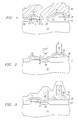
- Figures 1-7 are cross-sectional views of the fabrication of a semiconductor integrated circuit according to one embodiment of the present invention.
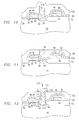
- Figures 8-12 are cross-sectional views of the fabrication of a semiconductor integrated circuit according to an alternative embodiment of the present invention.
- Figure 1 illustrates, in cross-section, a portion of an integrated circuit that has been partially fabricated.
- the present invention is directed to forming a contact opening which meets design criteria as such contacts are generally the most sensitive to the misalignment and design rules for spacing as described above.
- the present invention is further directed to increasing the planarity of the overall surface.
- Figure 1 illustrates a portion of a wafer which has a surface at which isolation structures and devices in adjacent active areas are to be formed.
- an integrated circuit is to be formed on a silicon substrate 10. It is contemplated, of course, that the present invention will also be applicable to the formation of other contacts, including, for example, contacts between metallization and polysilicon.
- the silicon substrate may be p- or n- doped silicon depending upon the location in the wafer where the isolation and active devices are to be formed.
- the structure of Figure 1 includes silicon substrate 10, into a surface of and above which is a field oxide region 12 for separating active regions or devices. Various active devices may be formed on or in the surface of the substrate as well as overlying the field oxide region 12.
- a gate electrode 14, formed from a first layer of polysilicon 18, is shown overlying a gate oxide 16.
- typically gate electrode 14 will have sidewall oxide spacers 20, lightly doped drain regions 22, 24 and source and drain or diffused regions 26, 28.
- an interconnect 30 having sidewall oxide spacers 32, 24 as is known in the art. Interconnect 30 typically will at least partially overlie field oxide region 12.
- the diffused or active region 28 is formed of opposite conductivity type from that of substrate 10.
- substrate 10 may be lightly doped p-type silicon and diffusion region 28 may be heavily doped n-type silicon.
- substrate 10 may instead be a well or tub region in a CMOS process, into which diffusion or active region 28 is formed.
- diffusion 28 is bounded by field oxide region 12, formed in the conventional manner.
- diffusion 28 is relatively shallow, such as on the order of 0.15 microns, as is conventional for modern integrated circuits having sub-micron feature sizes.
- diffusion 28 may be formed by ion implantation of the dopant followed by a high-temperature anneal to form the junction, as is well known in the art.
- the ion implantation may be performed prior to the formation of subsequent layers, with the drive-in anneal performed later in the process, if desired.
- a thin conformal dielectric layer 38 is deposited over the wafer surface overlying diffusion 28, field oxide region 12 and other already formed devices such as gate electrode 14 and interconnect 30.
- Layer 38 may be an undoped oxide layer preferably deposited at low temperatures, for example, between 250 to 700°C by chemical vapor deposition to a depth of about 500 to 1500 angstroms.
- a thick film 40 is deposited over the conformal dielectric layer 38. Thick film 40 is preferably polysilicon or other material having a relatively high etch selectivity over the underlying conformal dielectric layer 38. For purposes of illustration, thick film 40 will be referred to as polysilicon layer 40 and is preferably deposited to a thickness of about 10,000 to 15,000 angstroms.
- polysilicon layer 40 is patterned and etched to form polysilicon stacks 42, 44. These polysilicon stacks are formed at locations where contacts are to be made to underlying regions such as interconnect 30 and source/drain or diffused region 28.
- dielectric layer 46 is formed over the thin conformal dielectric layer 38 and over the polysilicon stacks 42, 44.
- Dielectric layer 46 is preferably borophosphorous silicate glass (BPSG) or other dielectric material which has a relatively high etch selectivity to the polysilicon stacks 42, 44 as well as the conformal dielectric layer 38.
- Dielectric layer 46 is formed for purposes of electrically isolating overlying conductive structures from all locations except where contacts are desired therebetween, for example where the polysilicon stacks are located over such regions as diffused area 28 and interconnect 30.
- Dielectric layer 46 preferably has a thickness of about 10,000 to 15,000 angstroms.
- dielectric layer 46 is etched to expose an upper surface of the polysilicon stacks 42, 44. If BPSG is used as dielectric layer 46, using a wet etch process with the etch rate of the BPSG over the polysilicon stacks of about 50:1 will allow an etch back of the dielectric layer 46 until the upper surface of the polysilicon stacks is reached or may allow for the BPSG layer to be etched below the upper surface of the polysilicon stacks to insure that the stacks are fully exposed.
- etch ratios and etch chemistries may be used to achieve a similar result, for example, chemical/mechanical polishing of dielectric layer 46 may result in a relatively planar etch back exposing the upper surface of the polysilicon stacks 42, 44.
- An additional alternative may be to form a composite dielectric layer 46 by forming spin-on-glass over the BPSG and partially etching the spin-on-glass and BPSG at a 1:1 etch ratio until the upper surfaces of the polysilicon stacks are exposed.
- Various etch back techniques known in the art such as those described above will accomplish the desired result of partially planarizing the structure and exposing the upper surface of the stacks.
- the polysilicon stacks 42, 44 are selectively etched by isotropic or anisotropic etching.
- the etch chemistry used will etch the polysilicon or other material used for the stacks at a high etch rate over the etch rate for the dielectric layer 46.
- Contact openings 48 and 50 will thus be formed through the dielectric layer 46 where the polysilicon stacks were formed, in this example, over diffused region 28 and interconnect 30.
- the thin conformed dielectric layer 38 acts as an etch stop during the polysilicon stack etch step to prevent the underlying active areas and devices from being etched away.
- conformal dielectric layer 38 helps to maintain the distance between the edge of the contact opening and the neighboring devices, thus maintaining required distances between devices and insuring device integrity as will be more fully described below with reference to an alternative embodiment.
- the thin conformal dielectric layer 38 is next etched from the contact openings 48, 50 exposing the active regions or devices in the contact openings.
- the conformal dielectric layer 38 is preferably removed by anisotropic etching to maintain the vertical dimensions or width of the contact opening.
- the dielectric or BPSG may be reflowed before or after etching the polysilicon stacks to increase the planarity of the dielectric layer.
- the polysilicon stacks were preferably patterned to have a width smaller than the width of the underlying active devices or regions, in this example, having a width of about 4000 angstroms.
- opening 50 is shown as misaligned over diffused region 28 toward the field oxide region 12. If this misalignment occurs over this active area, a portion of the field oxide region 12 at location 52 may be removed when the conformal dielectric layer 38 is removed from the contact opening 50 possibly reducing the area of contact between an overlying conductor and source/drain region 28.
- encroaching into the field oxide may also increase potential junction leakage problems.
- the stack may also be misaligned over the interconnect whereby it opens over one of the sidewall oxide spacers or it may open over the interconnect line and both sidewall oxide spacers.
- a thin layer of polysilicon 54 may be deposited on the dielectric layer 46 and in the openings 48 and 50.
- Polysilicon layer 54 is preferably deposited to a thickness which will permit filling the openings later with a conductive material to form an interconnect to the underlying active areas or devices, for example, if the opening is approximately 4000 angstroms, polysilicon layer 50 may be deposited to a thickness of about 1000 angstroms. Polysilicon layer 54 may then be doped to help prevent junction leakage if a misalignment occurs.
- Polysilicon layer 54 is doped with a similar dopant as the diffused region 24, such as by ion implantation or other suitable method. For example, if the source/drain region 28 has previously been doped with an N+ dopant such as arsenic, then polysilicon layer 54 may be doped with an N+ dopant such as phosphorous. As the polysilicon layer 54 is doped, dopants will diffuse into the substrate to some predetermined depth 56 based upon the dopant concentration and energy level. Doped region 56 will help to heal the junction region and prevent junction leakage.
- a conductive layer is formed over the polysilicon layer 54, patterned and etched as known in the art to form conductive contacts 58, 60 to the active areas and devices.
- Polysilicon layer 54 will typically be patterned and etched at the same time as the conductive contacts.
- Contacts 58, 60 may typically be aluminum, tungsten or other suitable contact material.
- the present invention provides for a contact opening which tolerates misalignment or oversized contact openings and insures device integrity by healing junction exposures.
- the thick film and polysilicon stacks provide for a more planar structure.
- Figure 8 illustrates, in cross-section, a portion of an integrated circuit that has been partially fabricated.
- the alternative embodiment of the present invention is also directed to forming a contact opening which meets design criteria but which is further capable of tolerating the sensitive misalignment problems and design rules for spacing as described above.
- Figure 8 illustrates a portion of a wafer which has a surface at which isolation structures and devices in adjacent active areas are to be formed.
- an integrated circuit is to be formed on a silicon substrate 70. It is again contemplated that the alternative embodiment will also be applicable to the formation of other contacts.
- the silicon substrate may be p- or n- doped silicon depending upon the location in the wafer where the isolation and active devices are to be formed.
- the structure of Figure 8 includes silicon substrate 70, into a surface of and above which is a field oxide region 72 for separating active regions or devices.
- Various active devices may be formed on or in the surface of the substrate as well as overlying the field oxide region 12.
- a gate oxide layer 74 is formed over the substrate and field oxide region.
- a doped polysilicon or polycide layer 76 is formed over the gate oxide layer as is known in the art.
- An undoped dielectric layer 78 such as oxide is formed over the polysilicon layer 76.
- these three layers 74, 76, 78 are patterned and etched to form interconnect 80 and gate electrode 88 as is known in the art.
- typically gate electrode 88 will have gate oxide 90, doped polysilicon layer 92, sidewall oxide spacers 96, lightly doped drain regions 97 and source and drain or diffused regions 98.
- gate electrode 88 will also have a capping layer 94 formed from the undoped oxide layer 78.
- interconnect 80 having a doped polysilicon layer 82 and sidewall oxide spacers 84 as is known in the art.
- a capping layer 86 formed from the undoped oxide layer 78.
- Interconnect 80 typically will at least partially overlie field oxide region 72.
- Capping layers 86, 94 will preferably have a thickness of about 1500 to 2000 angstroms.
- a thin conformal dielectric layer 100 is deposited over the wafer surface overlying diffusion region 98, field oxide region 72 and other already formed devices such as gate electrode 88 and interconnect 80.
- Conformal dielectric layer 100 is preferably an oxide layer deposited to a thickness of about 500 to 1500 angstroms. It is important, as will be discussed in detail below, that conformal dielectric layer 100 have a thickness less than the thickness of the capping layers 86, 94.
- a thick film 102 is deposited over the conformal dielectric layer 100. Thick film 102 is again preferably polysilicon or other material having a relatively high etch selectivity over the underlying conformal dielectric layer 100 and is preferably deposited to a thickness of about 10,000 to 15,000 angstroms.
- Dielectric layer 106 is formed over the thin conformal dielectric layer 100 and over the polysilicon stack 104. As described above, dielectric layer 106 is preferably borophosphorous silicate glass (BPSG) or other dielectric material which has a relatively high etch selectivity to the polysilicon stack 104 as well as the conformal dielectric layer 100. Dielectric layer 106 will electrically isolate the overlying conductive structures from all locations except where contacts are desired therebetween.
- BPSG borophosphorous silicate glass
- dielectric layer 106 is etched to expose an upper surface of the polysilicon stack 104.
- Various etch back techniques known in the art such as those described above will accomplish the desired result.
- the polysilicon stack 104 is etched by isotropic or anisotropic etching forming a contact opening 107 through the dielectric layer 106.
- Polysilicon stack in this example, is shown misaligned in the opposite direction over the source/drain region 98 and is partially aligned over the gate electrode 88.
- the thin conformal dielectric layer 100 is also etched from the contact opening 107 exposing the active area 98 in the contact opening.
- the conformal dielectric layer 100 is preferably removed by anisotropic etching to maintain the vertical dimensions or width of the contact opening. If misalignment of the gate electrode occurs in one direction and the contact opening is misaligned in the opposite direction, a cumulative error results.
- any misalignment of the contact opening 107 may decrease the contact space between the edge 109 of gate electrode 88 and the edge 111 of the contact opening 107. Due to the misalignment of the contact opening, in this example, effectively opening over the sidewall spacer 96, the distance between these active areas may be reduced enough such that the design rules for a metal contact space to gate cannot be tolerated to insure device integrity.
- the thickness of the capping layer 94 will insure that the required distance between the devices in order to maintain device integrity will be met.
- the thickness of the capping layer 94 must be greater than the thickness of the conformal dielectric layer 100 and thick enough that if the conformal dielectric layer 100 is overetched there will still remain enough capping layer to insure that design rules are met.
- the capping layer is about 1500 to 2000 angstroms while the conformal dielectric layer is about 1000 to 1500 angstroms.
- a polysilicon layer 108 may then be deposited to a thickness of about 1000 angstroms on the dielectric layer 106 and in the opening 107.
- Polysilicon layer 106 may then be doped to help prevent junction leakage.
- dopants will diffuse into the substrate to some predetermined depth 110.
- Doped region 110 will heal the junction region and prevent junction leakage.
- a conductive layer is then formed over the polysilicon layer 108, patterned and etched along with polysilicon layer 108 as known in the art to form a conductive contact 112 to the active area 98.
- opening the contact becomes a self-aligned feature such that the contact opening is now self-aligned to the gate.
- This self-aligned process can eliminate the conventional "dogbone” structure or larger enclosure needed, thereby increasing the density of devices on the integrated circuit. This process can also be used for other layers to eliminate the "dogbone” features and minimize the required design rules. As described above, in addition to the self-aligned benefit of the present invention, a more planar structure with high integrity junctions are achievable.
Landscapes
- Internal Circuitry In Semiconductor Integrated Circuit Devices (AREA)
- Electrodes Of Semiconductors (AREA)
Applications Claiming Priority (2)
| Application Number | Priority Date | Filing Date | Title |
|---|---|---|---|
| US282730 | 1994-07-29 | ||
| US08/282,730 US6297110B1 (en) | 1994-07-29 | 1994-07-29 | Method of forming a contact in an integrated circuit |
Publications (3)
| Publication Number | Publication Date |
|---|---|
| EP0696061A2 true EP0696061A2 (de) | 1996-02-07 |
| EP0696061A3 EP0696061A3 (de) | 1997-07-02 |
| EP0696061B1 EP0696061B1 (de) | 2005-10-26 |
Family
ID=23082878
Family Applications (1)
| Application Number | Title | Priority Date | Filing Date |
|---|---|---|---|
| EP95304825A Expired - Lifetime EP0696061B1 (de) | 1994-07-29 | 1995-07-11 | Herstellungsverfahren für einen Kontakt in einer integrierten Schaltung |
Country Status (4)
| Country | Link |
|---|---|
| US (2) | US6297110B1 (de) |
| EP (1) | EP0696061B1 (de) |
| JP (1) | JPH0878354A (de) |
| DE (1) | DE69534542D1 (de) |
Cited By (2)
| Publication number | Priority date | Publication date | Assignee | Title |
|---|---|---|---|---|
| EP0766301A3 (de) * | 1995-09-27 | 1998-04-15 | Siemens Aktiengesellschaft | Verfahren zur Herstellung von selbstausgerichteten Kontaktlöchern unter Verwendung einer Hilfsschicht aus Polysilizium |
| EP0890984A1 (de) * | 1997-06-30 | 1999-01-13 | Siemens Aktiengesellschaft | Doppel-damaszener Struktur und Verfahren zu ihrer Herstellung |
Families Citing this family (10)
| Publication number | Priority date | Publication date | Assignee | Title |
|---|---|---|---|---|
| US6730619B2 (en) * | 2000-06-15 | 2004-05-04 | Samsung Electronics Co., Ltd. | Method of manufacturing insulating layer and semiconductor device including insulating layer |
| JP2003297957A (ja) * | 2002-04-05 | 2003-10-17 | Mitsubishi Electric Corp | 半導体装置及び半導体装置の製造方法 |
| US20080096337A1 (en) * | 2006-10-06 | 2008-04-24 | Texas Instruments Incorporated | Disposable semiconductor device spacer with high selectivity to oxide |
| US7888252B2 (en) * | 2009-02-17 | 2011-02-15 | International Business Machines Corporation | Self-aligned contact |
| US8399183B2 (en) | 2009-05-13 | 2013-03-19 | Synopsys, Inc. | Patterning a single integrated circuit layer using automatically-generated masks and multiple masking layers |
| US8932911B2 (en) * | 2013-02-27 | 2015-01-13 | GlobalFoundries, Inc. | Integrated circuits and methods for fabricating integrated circuits with capping layers between metal contacts and interconnects |
| US9337094B1 (en) | 2015-01-05 | 2016-05-10 | International Business Machines Corporation | Method of forming contact useful in replacement metal gate processing and related semiconductor structure |
| US9685368B2 (en) * | 2015-06-26 | 2017-06-20 | Taiwan Semiconductor Manufacturing Company, Ltd. | Interconnect structure having an etch stop layer over conductive lines |
| US10157780B2 (en) * | 2016-11-29 | 2018-12-18 | Taiwan Semiconductor Manufacturing Company, Ltd. | Method of forming a device having a doping layer and device formed |
| TWI839046B (zh) * | 2022-12-26 | 2024-04-11 | 華邦電子股份有限公司 | 膜層中的縫隙的檢測方法 |
Family Cites Families (24)
| Publication number | Priority date | Publication date | Assignee | Title |
|---|---|---|---|---|
| DE453644C (de) | 1926-03-08 | 1927-12-13 | Friedrich Puppe | Verfahren zum Beschriften bildhafter Druckmuster unter Verwendung von abgedrucktem Letternsatz, den man in gewuenschter Groesse photographiert |
| US4888297A (en) * | 1982-09-20 | 1989-12-19 | International Business Machines Corporation | Process for making a contact structure including polysilicon and metal alloys |
| JPS6286853A (ja) * | 1985-10-14 | 1987-04-21 | Fujitsu Ltd | 半導体装置の製造方法 |
| US5236867A (en) * | 1987-11-13 | 1993-08-17 | Matsushita Electronics Corporation | Manufacturing method of contact hole arrangement of a semiconductor device |
| US4977108A (en) * | 1987-12-02 | 1990-12-11 | Advanced Micro Devices, Inc. | Method of making self-aligned, planarized contacts for semiconductor devices |
| US4868138A (en) | 1988-03-23 | 1989-09-19 | Sgs-Thomson Microelectronics, Inc. | Method for forming a self-aligned source/drain contact for an MOS transistor |
| US4966870A (en) * | 1988-04-14 | 1990-10-30 | International Business Machines Corporation | Method for making borderless contacts |
| US4986878A (en) * | 1988-07-19 | 1991-01-22 | Cypress Semiconductor Corp. | Process for improved planarization of the passivation layers for semiconductor devices |
| US4961822A (en) * | 1989-04-17 | 1990-10-09 | Liao Kuan Y | Fully recessed interconnection scheme with titanium-tungsten and selective CVD tungsten |
| US5026666A (en) * | 1989-12-28 | 1991-06-25 | At&T Bell Laboratories | Method of making integrated circuits having a planarized dielectric |
| EP0453644B1 (de) * | 1990-04-27 | 1995-05-10 | Siemens Aktiengesellschaft | Verfahren zur Herstellung einer Öffnung in einem Halbleiterschichtaufbau und dessen Verwendung zur Herstellung von Kontaktlöchern |
| JP2895167B2 (ja) * | 1990-05-31 | 1999-05-24 | キヤノン株式会社 | 半導体装置およびその製造方法 |
| US5022958A (en) * | 1990-06-27 | 1991-06-11 | At&T Bell Laboratories | Method of etching for integrated circuits with planarized dielectric |
| US5037777A (en) * | 1990-07-02 | 1991-08-06 | Motorola Inc. | Method for forming a multi-layer semiconductor device using selective planarization |
| KR920003461A (ko) * | 1990-07-30 | 1992-02-29 | 김광호 | 접촉영역 형성방법 및 그를 이용한 반도체장치의 제조방법 |
| US4997790A (en) * | 1990-08-13 | 1991-03-05 | Motorola, Inc. | Process for forming a self-aligned contact structure |
| US5158910A (en) * | 1990-08-13 | 1992-10-27 | Motorola Inc. | Process for forming a contact structure |
| JP2913918B2 (ja) * | 1991-08-26 | 1999-06-28 | 日本電気株式会社 | 半導体装置の製造方法 |
| US5268332A (en) * | 1992-11-12 | 1993-12-07 | At&T Bell Laboratories | Method of integrated circuit fabrication having planarized dielectrics |
| US5283208A (en) * | 1992-12-04 | 1994-02-01 | International Business Machines Corporation | Method of making a submicrometer local structure using an organic mandrel |
| US5359226A (en) * | 1993-02-02 | 1994-10-25 | Paradigm Technology, Inc. | Static memory with self aligned contacts and split word lines |
| US5854135A (en) * | 1997-04-09 | 1998-12-29 | Vanguard International Semiconductor Corporation | Optimized dry etching procedure, using an oxygen containing ambient, for small diameter contact holes |
| US6025255A (en) * | 1998-06-25 | 2000-02-15 | Vanguard International Semiconductor Corporation | Two-step etching process for forming self-aligned contacts |
| US6268281B1 (en) * | 1999-11-15 | 2001-07-31 | Taiwan Semiconductor Manufacturing Company | Method to form self-aligned contacts with polysilicon plugs |
-
1994
- 1994-07-29 US US08/282,730 patent/US6297110B1/en not_active Expired - Lifetime
-
1995
- 1995-07-11 DE DE69534542T patent/DE69534542D1/de not_active Expired - Lifetime
- 1995-07-11 EP EP95304825A patent/EP0696061B1/de not_active Expired - Lifetime
- 1995-07-28 JP JP7193742A patent/JPH0878354A/ja active Pending
-
2001
- 2001-08-07 US US09/923,746 patent/US6580133B2/en not_active Expired - Fee Related
Non-Patent Citations (1)
| Title |
|---|
| None |
Cited By (2)
| Publication number | Priority date | Publication date | Assignee | Title |
|---|---|---|---|---|
| EP0766301A3 (de) * | 1995-09-27 | 1998-04-15 | Siemens Aktiengesellschaft | Verfahren zur Herstellung von selbstausgerichteten Kontaktlöchern unter Verwendung einer Hilfsschicht aus Polysilizium |
| EP0890984A1 (de) * | 1997-06-30 | 1999-01-13 | Siemens Aktiengesellschaft | Doppel-damaszener Struktur und Verfahren zu ihrer Herstellung |
Also Published As
| Publication number | Publication date |
|---|---|
| DE69534542D1 (de) | 2005-12-01 |
| EP0696061A3 (de) | 1997-07-02 |
| US20020037622A1 (en) | 2002-03-28 |
| US6297110B1 (en) | 2001-10-02 |
| US6580133B2 (en) | 2003-06-17 |
| EP0696061B1 (de) | 2005-10-26 |
| JPH0878354A (ja) | 1996-03-22 |
Similar Documents
| Publication | Publication Date | Title |
|---|---|---|
| US5472897A (en) | Method for fabricating MOS device with reduced anti-punchthrough region | |
| EP0088922B1 (de) | Verfahren zum Herstellen von Elektroden und Verdrahtungsstreifen auf einer Halbleiteranordnung | |
| US6737308B2 (en) | Semiconductor device having LDD-type source/drain regions and fabrication method thereof | |
| US5406111A (en) | Protection device for an intergrated circuit and method of formation | |
| US5674760A (en) | Method of forming isolation regions in a MOS transistor device | |
| US5714393A (en) | Diode-connected semiconductor device and method of manufacture | |
| US6709950B2 (en) | Semiconductor device and method of manufacturing the same | |
| US6271065B1 (en) | Method directed to the manufacture of an SOI device | |
| US5874769A (en) | Mosfet isolation structure with planar surface | |
| US5612240A (en) | Method for making electrical connections to self-aligned contacts that extends beyond the photo-lithographic resolution limit | |
| KR20020011133A (ko) | 상감 세공 접촉 및 게이트 공정으로 제조된 자기-정렬소스 및 드레인 확장부 | |
| US5554554A (en) | Process for fabricating two loads having different resistance levels in a common layer of polysilicon | |
| US6297110B1 (en) | Method of forming a contact in an integrated circuit | |
| US5432105A (en) | Method for fabricating self-aligned polysilicon contacts on FET source/drain areas | |
| US5332913A (en) | Buried interconnect structure for semiconductor devices | |
| US5866459A (en) | Method of fabricating a contact structure for an MOS transistor entirely on isolation oxide | |
| EP0513639A2 (de) | Halbleiter-Feldeffekttransistoranordnung und ihr Herstellungsverfahren | |
| US6287911B1 (en) | Semiconductor device with silicide layers and fabrication method thereof | |
| US6034410A (en) | MOSFET structure with planar surface | |
| US5716886A (en) | Method of fabricating a high voltage metal-oxide semiconductor (MOS) device | |
| KR100293052B1 (ko) | 반도체 소자 제조 방법 | |
| US5707721A (en) | Methods of forming field effect transistors having oxidation-controlled gate lengths | |
| KR100333361B1 (ko) | 반도체장치의 제조방법 | |
| US5652160A (en) | Method of fabricating a buried contact structure with WSix sidewall spacers | |
| US20020033536A1 (en) | Semiconductor device and manufacturing method thereof |
Legal Events
| Date | Code | Title | Description |
|---|---|---|---|
| PUAI | Public reference made under article 153(3) epc to a published international application that has entered the european phase |
Free format text: ORIGINAL CODE: 0009012 |
|
| AK | Designated contracting states |
Kind code of ref document: A2 Designated state(s): DE FR GB IT |
|
| PUAL | Search report despatched |
Free format text: ORIGINAL CODE: 0009013 |
|
| AK | Designated contracting states |
Kind code of ref document: A3 Designated state(s): DE FR GB IT |
|
| 17P | Request for examination filed |
Effective date: 19971219 |
|
| RAP3 | Party data changed (applicant data changed or rights of an application transferred) |
Owner name: STMICROELECTRONICS, INC. |
|
| 17Q | First examination report despatched |
Effective date: 20020823 |
|
| GRAP | Despatch of communication of intention to grant a patent |
Free format text: ORIGINAL CODE: EPIDOSNIGR1 |
|
| GRAS | Grant fee paid |
Free format text: ORIGINAL CODE: EPIDOSNIGR3 |
|
| GRAA | (expected) grant |
Free format text: ORIGINAL CODE: 0009210 |
|
| AK | Designated contracting states |
Kind code of ref document: B1 Designated state(s): DE FR GB IT |
|
| PG25 | Lapsed in a contracting state [announced via postgrant information from national office to epo] |
Ref country code: IT Free format text: LAPSE BECAUSE OF FAILURE TO SUBMIT A TRANSLATION OF THE DESCRIPTION OR TO PAY THE FEE WITHIN THE PRESCRIBED TIME-LIMIT;WARNING: LAPSES OF ITALIAN PATENTS WITH EFFECTIVE DATE BEFORE 2007 MAY HAVE OCCURRED AT ANY TIME BEFORE 2007. THE CORRECT EFFECTIVE DATE MAY BE DIFFERENT FROM THE ONE RECORDED. Effective date: 20051026 |
|
| REG | Reference to a national code |
Ref country code: GB Ref legal event code: FG4D |
|
| REF | Corresponds to: |
Ref document number: 69534542 Country of ref document: DE Date of ref document: 20051201 Kind code of ref document: P |
|
| PG25 | Lapsed in a contracting state [announced via postgrant information from national office to epo] |
Ref country code: DE Free format text: LAPSE BECAUSE OF FAILURE TO SUBMIT A TRANSLATION OF THE DESCRIPTION OR TO PAY THE FEE WITHIN THE PRESCRIBED TIME-LIMIT Effective date: 20060127 |
|
| ET | Fr: translation filed | ||
| PLBE | No opposition filed within time limit |
Free format text: ORIGINAL CODE: 0009261 |
|
| STAA | Information on the status of an ep patent application or granted ep patent |
Free format text: STATUS: NO OPPOSITION FILED WITHIN TIME LIMIT |
|
| 26N | No opposition filed |
Effective date: 20060727 |
|
| PGFP | Annual fee paid to national office [announced via postgrant information from national office to epo] |
Ref country code: GB Payment date: 20070711 Year of fee payment: 13 |
|
| PGFP | Annual fee paid to national office [announced via postgrant information from national office to epo] |
Ref country code: FR Payment date: 20070710 Year of fee payment: 13 |
|
| GBPC | Gb: european patent ceased through non-payment of renewal fee |
Effective date: 20080711 |
|
| REG | Reference to a national code |
Ref country code: FR Ref legal event code: ST Effective date: 20090331 |
|
| PG25 | Lapsed in a contracting state [announced via postgrant information from national office to epo] |
Ref country code: GB Free format text: LAPSE BECAUSE OF NON-PAYMENT OF DUE FEES Effective date: 20080711 |
|
| PG25 | Lapsed in a contracting state [announced via postgrant information from national office to epo] |
Ref country code: FR Free format text: LAPSE BECAUSE OF NON-PAYMENT OF DUE FEES Effective date: 20080731 |