EP0513639A2 - Halbleiter-Feldeffekttransistoranordnung und ihr Herstellungsverfahren - Google Patents
Halbleiter-Feldeffekttransistoranordnung und ihr Herstellungsverfahren Download PDFInfo
- Publication number
- EP0513639A2 EP0513639A2 EP92107591A EP92107591A EP0513639A2 EP 0513639 A2 EP0513639 A2 EP 0513639A2 EP 92107591 A EP92107591 A EP 92107591A EP 92107591 A EP92107591 A EP 92107591A EP 0513639 A2 EP0513639 A2 EP 0513639A2
- Authority
- EP
- European Patent Office
- Prior art keywords
- gate electrodes
- isolation
- gate
- regions
- trenches
- Prior art date
- Legal status (The legal status is an assumption and is not a legal conclusion. Google has not performed a legal analysis and makes no representation as to the accuracy of the status listed.)
- Ceased
Links
Images



Classifications
-
- H—ELECTRICITY
- H10—SEMICONDUCTOR DEVICES; ELECTRIC SOLID-STATE DEVICES NOT OTHERWISE PROVIDED FOR
- H10D—INORGANIC ELECTRIC SEMICONDUCTOR DEVICES
- H10D30/00—Field-effect transistors [FET]
- H10D30/01—Manufacture or treatment
- H10D30/021—Manufacture or treatment of FETs having insulated gates [IGFET]
- H10D30/0223—Manufacture or treatment of FETs having insulated gates [IGFET] having source and drain regions or source and drain extensions self-aligned to sides of the gate
- H10D30/0227—Manufacture or treatment of FETs having insulated gates [IGFET] having source and drain regions or source and drain extensions self-aligned to sides of the gate having both lightly-doped source and drain extensions and source and drain regions self-aligned to the sides of the gate, e.g. lightly-doped drain [LDD] MOSFET or double-diffused drain [DDD] MOSFET
-
- H—ELECTRICITY
- H10—SEMICONDUCTOR DEVICES; ELECTRIC SOLID-STATE DEVICES NOT OTHERWISE PROVIDED FOR
- H10D—INORGANIC ELECTRIC SEMICONDUCTOR DEVICES
- H10D64/00—Electrodes of devices having potential barriers
- H10D64/20—Electrodes characterised by their shapes, relative sizes or dispositions
- H10D64/27—Electrodes not carrying the current to be rectified, amplified, oscillated or switched, e.g. gates
- H10D64/311—Gate electrodes for field-effect devices
- H10D64/411—Gate electrodes for field-effect devices for FETs
- H10D64/511—Gate electrodes for field-effect devices for FETs for IGFETs
-
- H—ELECTRICITY
- H10—SEMICONDUCTOR DEVICES; ELECTRIC SOLID-STATE DEVICES NOT OTHERWISE PROVIDED FOR
- H10D—INORGANIC ELECTRIC SEMICONDUCTOR DEVICES
- H10D84/00—Integrated devices formed in or on semiconductor substrates that comprise only semiconducting layers, e.g. on Si wafers or on GaAs-on-Si wafers
- H10D84/01—Manufacture or treatment
- H10D84/0123—Integrating together multiple components covered by H10D12/00 or H10D30/00, e.g. integrating multiple IGBTs
- H10D84/0126—Integrating together multiple components covered by H10D12/00 or H10D30/00, e.g. integrating multiple IGBTs the components including insulated gates, e.g. IGFETs
- H10D84/0165—Integrating together multiple components covered by H10D12/00 or H10D30/00, e.g. integrating multiple IGBTs the components including insulated gates, e.g. IGFETs the components including complementary IGFETs, e.g. CMOS devices
- H10D84/0186—Manufacturing their interconnections or electrodes, e.g. source or drain electrodes
-
- H—ELECTRICITY
- H10—SEMICONDUCTOR DEVICES; ELECTRIC SOLID-STATE DEVICES NOT OTHERWISE PROVIDED FOR
- H10D—INORGANIC ELECTRIC SEMICONDUCTOR DEVICES
- H10D84/00—Integrated devices formed in or on semiconductor substrates that comprise only semiconducting layers, e.g. on Si wafers or on GaAs-on-Si wafers
- H10D84/01—Manufacture or treatment
- H10D84/0123—Integrating together multiple components covered by H10D12/00 or H10D30/00, e.g. integrating multiple IGBTs
- H10D84/0126—Integrating together multiple components covered by H10D12/00 or H10D30/00, e.g. integrating multiple IGBTs the components including insulated gates, e.g. IGFETs
- H10D84/0165—Integrating together multiple components covered by H10D12/00 or H10D30/00, e.g. integrating multiple IGBTs the components including insulated gates, e.g. IGFETs the components including complementary IGFETs, e.g. CMOS devices
- H10D84/0188—Manufacturing their isolation regions
-
- H—ELECTRICITY
- H10—SEMICONDUCTOR DEVICES; ELECTRIC SOLID-STATE DEVICES NOT OTHERWISE PROVIDED FOR
- H10D—INORGANIC ELECTRIC SEMICONDUCTOR DEVICES
- H10D84/00—Integrated devices formed in or on semiconductor substrates that comprise only semiconducting layers, e.g. on Si wafers or on GaAs-on-Si wafers
- H10D84/01—Manufacture or treatment
- H10D84/02—Manufacture or treatment characterised by using material-based technologies
- H10D84/03—Manufacture or treatment characterised by using material-based technologies using Group IV technology, e.g. silicon technology or silicon-carbide [SiC] technology
- H10D84/038—Manufacture or treatment characterised by using material-based technologies using Group IV technology, e.g. silicon technology or silicon-carbide [SiC] technology using silicon technology, e.g. SiGe
-
- H—ELECTRICITY
- H10—SEMICONDUCTOR DEVICES; ELECTRIC SOLID-STATE DEVICES NOT OTHERWISE PROVIDED FOR
- H10W—GENERIC PACKAGES, INTERCONNECTIONS, CONNECTORS OR OTHER CONSTRUCTIONAL DETAILS OF DEVICES COVERED BY CLASS H10
- H10W10/00—Isolation regions in semiconductor bodies between components of integrated devices
- H10W10/01—Manufacture or treatment
- H10W10/011—Manufacture or treatment of isolation regions comprising dielectric materials
- H10W10/014—Manufacture or treatment of isolation regions comprising dielectric materials using trench refilling with dielectric materials, e.g. shallow trench isolations
- H10W10/0145—Manufacture or treatment of isolation regions comprising dielectric materials using trench refilling with dielectric materials, e.g. shallow trench isolations of trenches having shapes other than rectangular or V-shape
-
- H—ELECTRICITY
- H10—SEMICONDUCTOR DEVICES; ELECTRIC SOLID-STATE DEVICES NOT OTHERWISE PROVIDED FOR
- H10W—GENERIC PACKAGES, INTERCONNECTIONS, CONNECTORS OR OTHER CONSTRUCTIONAL DETAILS OF DEVICES COVERED BY CLASS H10
- H10W10/00—Isolation regions in semiconductor bodies between components of integrated devices
- H10W10/10—Isolation regions comprising dielectric materials
- H10W10/17—Isolation regions comprising dielectric materials formed using trench refilling with dielectric materials, e.g. shallow trench isolations
-
- H—ELECTRICITY
- H10—SEMICONDUCTOR DEVICES; ELECTRIC SOLID-STATE DEVICES NOT OTHERWISE PROVIDED FOR
- H10P—GENERIC PROCESSES OR APPARATUS FOR THE MANUFACTURE OR TREATMENT OF DEVICES COVERED BY CLASS H10
- H10P30/00—Ion implantation into wafers, substrates or parts of devices
- H10P30/20—Ion implantation into wafers, substrates or parts of devices into semiconductor materials, e.g. for doping
- H10P30/202—Ion implantation into wafers, substrates or parts of devices into semiconductor materials, e.g. for doping characterised by the semiconductor materials
- H10P30/204—Ion implantation into wafers, substrates or parts of devices into semiconductor materials, e.g. for doping characterised by the semiconductor materials into Group IV semiconductors
-
- H—ELECTRICITY
- H10—SEMICONDUCTOR DEVICES; ELECTRIC SOLID-STATE DEVICES NOT OTHERWISE PROVIDED FOR
- H10P—GENERIC PROCESSES OR APPARATUS FOR THE MANUFACTURE OR TREATMENT OF DEVICES COVERED BY CLASS H10
- H10P30/00—Ion implantation into wafers, substrates or parts of devices
- H10P30/20—Ion implantation into wafers, substrates or parts of devices into semiconductor materials, e.g. for doping
- H10P30/21—Ion implantation into wafers, substrates or parts of devices into semiconductor materials, e.g. for doping of electrically active species
-
- H—ELECTRICITY
- H10—SEMICONDUCTOR DEVICES; ELECTRIC SOLID-STATE DEVICES NOT OTHERWISE PROVIDED FOR
- H10P—GENERIC PROCESSES OR APPARATUS FOR THE MANUFACTURE OR TREATMENT OF DEVICES COVERED BY CLASS H10
- H10P30/00—Ion implantation into wafers, substrates or parts of devices
- H10P30/20—Ion implantation into wafers, substrates or parts of devices into semiconductor materials, e.g. for doping
- H10P30/28—Ion implantation into wafers, substrates or parts of devices into semiconductor materials, e.g. for doping characterised by an annealing step, e.g. for activation of dopants
Definitions
- the present invention is concerned with semiconductor field effect transistor devices and a method for fabricating the devices, and is especially concerned with devices wherein the gate is self-aligned and butted against the trench isolation.
- the present invention is particularly advantageous in obtaining ultra-compact and high performance devices.
- the field effect transistor is an important electrical switching device in large scale integrated circuits. Such circuits may contain as many as one million or more FETs on a single semiconductor chip. Such chips typically measure, today, approximately one-half of one inch on each side.
- the physical size (i.e., the lateral dimensions) of the FET is an important factor in determining how closely, devices may be packed into a given chip area.
- the speed of operation of a circuit is determined in part by the size of the individual FET elements, especially the length of the gate electrode. Accordingly, continuing work is being carried out to provide new procedures which will yield smaller and faster FET structures.
- Object of the present invention as claimed is to provide a technique capable of fabricating ultra-compact FET devices whereby the gate electrode is self-aligned and butted against the trench isolation.
- the present invention provides for achieving contacts which fully overlap the gate at the same time as providing contacts which overlap fully the source and drain regions.
- the present invention is concerned with a semiconductor device that comprises a semiconductor substrate having therein channel regions that contain active impurities of a first conductive type. Located over the channel regions is a dielectric layer and over the dielectric layer are patterned gate electrodes. Doped source and drain regions of a second and opposite conductivity type are self-aligned with respect to the ends of the gate electrode in the length direction. Isolation trenches containing isolating material are provided as well as isolation to the sidewalls of the gate electrodes. The gate electrodes are self-aligned in the width direction to the isolation trenches such that the gates are butted against the isolation trenches without overlap. An insulating layer is present over the entire substrate except where contact windows to the gate electrodes and source and drain regions are provided. Metallic-type high conductivity electrical interconnection tracks are also provided which contact through the contact windows to the gate electrodes and source and drain regions.
- the process aspect of the present invention is concerned with a method for fabricating a semiconductor device which comprises the following steps:
- An advantage of the present invention is that it overcomes the problems inherent to conventional isolation techniques which occur as the device width approaches 0.1 micron dimensions.
- the technique of local oxidation of silicon (LOCOS) gives rise to a well-known "bird's beak" profile around the perimeter of the device (see Figure 1), which due to charge sharing effects leads to a well-known but undesirable variation in threshold voltage as the device width is reduced.
- Conventional trench isolation techniques solve this problem by providing an abrupt interface between device and isolation but are susceptible to parasitic FET operation at the abrupt corners of the device where the threshold voltage is effectively lowered due to increased electric field strength associated with the gate-to-trench overlap (see Figure 2).
- the present invention uses a similar approach to conventional trench isolation, in that it avoids formation of a "bird's beak,” but differs in that there is no overlap between the gate and the trench thereby avoiding parasitic FET operation (see Figure 3).
- gate contacts are made directly to the active gate electrode. Whilst the concept of a direct metallic-type contact to the active gate electrode is known to the art, the structure and suitable mode of fabrication of such contacts are unique to the present invention. Such direct gate contacts provide further advantage for ultra-small FETs in that a gate electrode RC time constant associated with current flow along the gate, in the width direction of the device, is eliminated and, additionally, the area required for a gate contact pad is eliminated which leads to improved packing density.
- a further advantage of the present invention over conventional trench isolated devices is that the well-known difficulties associated with substrate planarization which normally follow deposition of the trench insulation material can be eliminated. Such planarization is usually required prior to deposition and delineation of the gate electrodes since they are required to traverse onto the trench isolation where a gate contact pad is provided for connection to the interconnect metalization.
- the discussion of the fabrication steps is directed to the aspects of using a P-type silicon substrate as the semiconductor substrate and N-type impurities in the source and drain regions leading to N-channel FET technology. Accordingly, it is understood that an N-type substrate and P-type impurities in the source and drain regions could be employed pursuant to the present invention leading to P-channel FET technology.
- N-channel and P-channel devices could be combined onto a N-well, P-well or twin-well substrate using well-established techniques as described in the prior art, to obtain Complementary FET technology.
- complementary FET technology applied at 0.25 micron ground rules, see Davari et al., "A High Performance 0.25 ⁇ m CMOS Technology," IEDM Technical Digest, December 1988, page 56.
- the process steps are applicable to P-type impurities and vice versa.
- the present invention is applicable to substrates other than silicon and to gate structures other than polycrystalline silicon.
- the terms “polysilicon” and “polycrystalline silicon” are used here interchangeably as in the prior art.
- the terms “metallic-type interconnection” or “high electrical conductivity interconnection” refer to tracks or lines of a metal, such as aluminum or tungsten, as well as to nonmetallic materials such as highly doped polysilicon or intermetallic silicides which nevertheless can have conductivities of the magnitude generally possessed by metals.
- first type refers to N or P-type impurities
- second type refers to the opposite conductivity type. That is, if the "first type” is P, then the “second type” is N. If the "first type” is N, then the “second type” is P.
- gate and “gate electrode” are interchangeable.
- the “length direction” of the device it is understood to refer to the direction from the source region to the drain region or visa versa.
- the “width direction” is understood to be that direction which is orthogonal to the "length direction” and in the plane of the initial substrate interface.
- a fragment of a semiconductor substrate 1 which can typically be a silicon substrate having any desired crystal orientation but more normally ( ⁇ 100>) orientation.
- a gate dielectric layer 2 is provided on the substrate 1, typically an ultrathin silicon dioxide layer of about 2.5 to about 5 nanometers. Such can be formed by thermal oxidation of the silicon substrate for example at about 800°C in the presence of dry oxygen.
- the desired channel impurity profiles are provided by ion implantation, either before or after formation of the ultra-thin dielectric layer.
- ion implantation either before or after formation of the ultra-thin dielectric layer.
- P-type dopant for the channel region of the device boron, aluminum, gallium, or indium could be used.
- a boron implant of about 1 X 10¹² to 5 x 10¹² atoms/cm2 at an energy of about 15 to about 30 keV is required for a device with a 0.1 micron gate electrode.
- the gate material 3 is deposited and patterned.
- a layer of polycrystalline silicon is deposited.
- the polysilicon layer is typically about 100 to 150 nanometers thick, and may be deposited by low pressure chemical-vapor deposition.
- the polysilicon layer is typically doped with an N-type dopant such as arsenic or phosphorus using ion implantation.
- the polysilicon is patterned using lithographic and etching techniques. In view of the process of the present invention, the polysilicon can be patterned with ultrasmall gate structures with dimensions as small as 0.1 microns or less.
- a gate pattern determining layer such as a layer of photoresist material of the type employed in known lithographic masking and etching techniques can be placed over the polysilicon gate material.
- a gate pattern determining layer such as a layer of photoresist material of the type employed in known lithographic masking and etching techniques can be placed over the polysilicon gate material.
- Any of the well-known photosensitive resist materials known to the art may be used.
- Application of the photoresist and appropriate lithographic procedures are well-known and described in the prior art. Such procedures are likely to be based on Gaussian or shaped electron beam lithography, X-ray printing, phase-shift optical printing or any other technique capable of resolving 0.1 micron images.
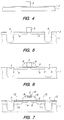
- Patterning of the gate electrodes into the polysilicon layer can be performed by well-known dry etching techniques such as reactive ion etching or electron-cyclotron resonance etching. Such techniques employ conditions that selectively and anisotropically etch the polysilicon without etching the underlying gate dielectric layer. Also, a wide variety of process gases and etch conditions are suitable, but typically a process with chlorine, bromine or fluorine containing gases is used. This results in delineation of the polysilicon gate 3 as illustrated in figure 4. After the gate is defined, the photoresist material above the patterned gate is then removed, typically by oxygen plasma ashing.
- the source and drain regions are formed, self-aligned to the gate structures 3, by thermal diffusion or ion implantation into the substrate or well region in the case of complementary FET technology.
- N-type impurities for silicon arsenic, phosphorus, or antimony can be employed.
- P-type impurities for silicon boron, aluminum, gallium, or indium can be employed.
- the source and drain regions are preferably ion implanted to provide ultra shallow junction profiles such as to a depth of about 50 to about 75 nanometers.
- an ultra shallow N-type region can be formed by an antimony implant of about 1 X 10¹⁴ to about 5 x 10¹⁴ atoms/cm2 at an energy typically in the range of about 5 to about 25 keV.
- the source 4 and drain 5 regions are illustrated in figure 5.
- isolation trenches are formed to provide electrical isolation between devices. These are formed by lithographically masking the active areas of the devices and then etching trenches 6 into the substrate (see Figure 6).
- the trench images are defined into a photoresist layer, aligned with respect to the gate level to within a given misregistration tolerance.
- the resist image can be used directly as etch mask during the trench etching procedure; however, there are certain advantages in using an intermediate pattern transfer mask of, for example, silicon nitride.
- Such a mask provides superior etch masking properties compared to photoresist since mask erosion and faceting effects are reduced and, in addition, it can be used as an oxidation mask for a selective trench sidewall oxidation as discussed later.
- Such a mask can be formed by low pressure chemical vapor deposition of silicon nitride prior to application of the photoresist.
- the transfer mask would be formed by reactive ion etching in a well-known methyl-trifluoride process.
- the isolation trenches 6 are etched using the nitride pattern transfer layer as a mask. This is achieved using a multiple step reactive ion etching process whereby the process first cuts through the gate electrodes where they overlap the trench regions. This is an essential feature of the device process in that it provides self-alignment of the gate electrode, in the width direction, so that it butts against the isolation trench without overlap.
- the trench reactive ion etching process is required to etch polysilicon, gate dielectric and substrate silicon and a bromine or chlorine based process can be used. If the process exhibits high etch selectivity with respect to the gate dielectric then it is necessary to interrupt the trench etching process after the gate polysilicon gate electrode has been etched, in order to etch the underlying gate dielectric using a short methyl-trifluoride etch, after which the trench etch can be continued to completion.
- the resulting trenches have substantially vertical surfaces in the silicon substrate 1.
- the trenches are likely to be of fixed width although variable width trenches could be employed. In the case of fixed width trenches, the trench width is likely to be about 0.1 to 0.15 microns and the depth in the range 0.25 to 0.5 microns.
- a passivating layer such as silicon dioxide, is grown on at least the vertical sidewalls of the trench.
- a passivating layer such as silicon dioxide, is grown on at least the vertical sidewalls of the trench.
- nitride is used as an intermediate trench etch mask, it provides protection for the horizontal surfaces of the device during this oxidation step.
- the thickness of such an oxide passivation is likely to be about 10 nanometers, preferably formed by dry oxidation at about 700 to 750°C. A relatively low oxidation temperature is chosen to avoid significant redistribution of the source and drain region impurities.
- the silicon nitride, if present, is then stripped using a phosphoric acid wet etching step.
- the trenches are filled with insulating material 7 using a well-known conformal deposition technique such as low pressure chemical vapor deposition in a tetra-ethoxy-silane ambient.
- oxide will form over the entire substrate and the gate structures.
- the insulating layer is then etched back, using an anisotropic oxide reactive ion etching process, to leave the trenches filled with insulating material and insulating layers 8 on the sidewalls of the gates (Fig. 6).
- the thickness of the sidewall is likely to be approximately 0.1 microns. This insulating material on the sidewalls of the gate acts to compensate for possible misalignment of masks when producing contact windows in the subsequent steps to provide for metallic-type interconnection to the gate electrode.
- a second source 10 and drain 11 can be provided by thermal diffusion or preferably by ion implantation to a depth of about 100 nanometers. Such is not necessary but preferred in order to improve the structure by lowering the resistance between the contacts and channel region and thereby increasing the performance of the device. Typically such can be provided by ion implantation of arsenic with a dose of about 5 x 10¹⁵ atom/cm2 at an energy of approximately 25 keV.
- a self-aligned silicidation of the gate, source and drain regions can be carried out to provide silicide layer 12. Such is not essential but could be used to reduce the contact resistance between the subsequently to be applied metallic-type interconnection to the gate electrode and the source and drain.
- the silicidation can be performed by well known techniques based upon metal deposition, reaction at elevated temperature and selective wet etching of non-reacted metal. The process is self-aligned in that silicide does not form over the trench isolation and gate sidewalls. See Figure 7. Metals such as titanium, tungsten, tantalum, platinum or cobalt may be used but more typically titanium is used. Typically, a silicide thickness, after reaction, of approximately 10 to 15 nanometers would be used.
- titanium silicide this could be formed by first sputter depositing a layer of titanium which is rapid thermal annealed to form silicide at the silicon source and drain regions and also over the polysilicon gate electrodes. Typically, this might be a 30 second anneal at 600°C in a nitrogen ambient. Next, a selective wet etch, such as a solution of hydrogen peroxide and sulfuric acid, is used to remove the unreacted titanium leaving only the required titanium silicide. Finally, the silicidation process is completed with a second rapid thermal annealing step which serves to reduce the sheet resistivity of the silicide regions. Typical conditions for this second anneal are 60 seconds at 800°C again in the presence of nitrogen.
- an insulating layer 13 is deposited to provide isolation from the subsequently to be deposited metallic-type interconnects (Fig. 8).
- the material used for this layer is preferably one which has different reactive ion etching properties to insulating materials 7 and 8.
- insulating materials 7 and 8 are silicon dioxide
- insulating material 13 can be silicon nitride.
- the silicon nitride can be provided by chemical vapor deposition using one of several well known processes. Typically, such a layer is about 0.1 to 0.2 microns thick.
- Contact windows to the gate electrodes and source and drain regions are delineated, again using lithographic techniques to define a photoresist image which is used as a reactive ion etch mask.
- the contact windows are defined such that they are designed with a finite overlap to the gate sidewalls (in the case of the gate contact) and the trench isolation (in the case of the source and drain contacts). This finite overlap is designed to be equal to the maximum allowed level to level misregistration and is likely to be ⁇ 0.025 microns for 0.1 micron lithography. This ensures that the gate, source and drain contact windows overlap the maximum available area of the regions to be contacted by the subsequently to be deposited metallic type interconnection. This is of particular importance for ultra-small devices as pursuant to the present invention since specific contact resistance is potentially a significant device parasitic.
- layer 13 is etched under conditions which provide selectivity with respect to the material of 7 and 8 so that the necessary contact windows to the gate, source and drain regions can be defined to overlap such material without risk of etching into the gate sidewalls, in the case of the gate contact, or the isolation trenches in the case of the source and drain contacts.
- this overlap provides compensation for misregistration between the contact lithography level and previous levels and is chosen to be equal to the maximum misregistration.
- Such an approach leads to gate, source and drain contacts which overlap fully the respective regions to be contacted. Whilst such approaches are known in the art for source and drain regions only, the present invention makes use of the gate sidewalls 8 to extend the technique to include gate contacts.
- a thin layer beneath 13 of a different material such as aluminum oxide, as known in the art, can be provided as an etch stop.
- the aluminum oxide would protect the isolation in the trenches and on the sidewalls of the gate since etching would stop once the thin layer was reached. The aluminum oxide would then be removed by known wet etching techniques without effecting the materials 7 and 8.
- the metallic-type high conductivity electrical interconnection 14 to the gate structure and, source and drain regions is formed.
- An example of a highly-conductive material commonly used for such interconnections is aluminum which may contain relatively small amounts of impurities to reduce electromigration effects or reduce chemical reactions between the aluminum and the semiconductor to be contacted.
- the interconnect material will be a refractory metal such as tungsten or possibly a stack of materials with a refractory metal closest to the semiconducting material.
- Such refractory materials provide superior contact reliability which is of particular importance to the present invention in that direct contact is made to the gate electrode.
- Such interconnect materials can be deposited by sputtering, chemical vapor deposition or by evaporation. Once deposited, the interconnect patterns are delineated using a patterned photoresist image as mask for a reactive ion etching step designed to etch the unmasked interconnect material. See Figure 8.
- FIG 9 illustrates a plan view of a field effect transistor pursuant to the present invention demonstrating the ultra small dimensions which may be achieved.
- Like numerals represent the same features as discussed above in figures 4 and 8. For instance, assuming the above desire for a fully scaled 0.1 micron device, the device has an active area with dimensions of 0.7 x 0.15 microns, separated from adjacent devices by a 0.15 micron wide isolation trench. At these dimensions, the device requires misregistrations to be less than or equal to ⁇ 0.025 microns for consecutive lithographic levels.
- Figures 10 and 11 illustrate the gate contact region of the device in cross-section, clarifying the approach used in the present invention to achieve fully overlapped gate contacts which are capable of accommodating misregistration.
- Figure 10 shows perfect registration between the gate contact and the gate electrode.
- Figure 11 shows the maximum misregistration which can be tolerated whilst still maintaining full overlap of the gate electrode.
Landscapes
- Insulated Gate Type Field-Effect Transistor (AREA)
- Element Separation (AREA)
- Metal-Oxide And Bipolar Metal-Oxide Semiconductor Integrated Circuits (AREA)
Applications Claiming Priority (2)
| Application Number | Priority Date | Filing Date | Title |
|---|---|---|---|
| US70124891A | 1991-05-16 | 1991-05-16 | |
| US701248 | 1991-05-16 |
Publications (2)
| Publication Number | Publication Date |
|---|---|
| EP0513639A2 true EP0513639A2 (de) | 1992-11-19 |
| EP0513639A3 EP0513639A3 (en) | 1992-12-23 |
Family
ID=24816586
Family Applications (1)
| Application Number | Title | Priority Date | Filing Date |
|---|---|---|---|
| EP19920107591 Ceased EP0513639A3 (en) | 1991-05-16 | 1992-05-06 | Semiconductor field effect transistor device and fabrication thereof |
Country Status (2)
| Country | Link |
|---|---|
| EP (1) | EP0513639A3 (de) |
| JP (1) | JPH05109762A (de) |
Cited By (11)
| Publication number | Priority date | Publication date | Assignee | Title |
|---|---|---|---|---|
| EP0615282A3 (de) * | 1993-03-10 | 1996-12-11 | Samsung Electronics Co Ltd | Verfahren zur Herstellung von MOSFET's mit von der Wanne gescheidenem Kanal. |
| EP0756320A3 (de) * | 1995-07-27 | 1998-04-01 | Matsushita Electric Industrial Co., Ltd. | Halbleiteranordnung und Verfahren zu ihrer Herstellung |
| WO1998032176A1 (en) * | 1997-01-21 | 1998-07-23 | Advanced Micro Devices, Inc. | As/P HYBRID nLDD JUNCTION AND MEDIUM Vdd OPERATION FOR HIGH SPEED MICROPROCESSORS |
| US5804862A (en) * | 1995-02-21 | 1998-09-08 | Nec Corporation | Semiconductor device having contact hole open to impurity region coplanar with buried isolating region |
| WO1998053497A1 (en) * | 1997-05-22 | 1998-11-26 | Advanced Micro Devices, Inc. | Method for mos transistor isolation |
| WO1999035685A1 (en) * | 1998-01-05 | 1999-07-15 | Advanced Micro Devices, Inc. | Integrated cmos transistor formation |
| EP0977265A1 (de) * | 1998-07-30 | 2000-02-02 | STMicroelectronics S.r.l. | Schaltkreis mit einem parasitären Transistor hoher Einsatzspannung |
| EP1787318A4 (de) * | 2004-08-10 | 2008-10-01 | Wafermasters Inc | Verfahren zur bildung von ultraflachen verbindungen |
| JP2014131073A (ja) * | 2001-07-17 | 2014-07-10 | Renesas Electronics Corp | 半導体装置及びその製造方法 |
| KR20230174699A (ko) * | 2022-06-21 | 2023-12-28 | 넥스칩 세미컨덕터 코퍼레이션 | 반도체 소자 및 그 제조 방법 |
| US12635486B2 (en) | 2022-06-21 | 2026-05-19 | Nexchip Semiconductor Corporation | Semiconductor device and manufacturing method thereof |
Families Citing this family (2)
| Publication number | Priority date | Publication date | Assignee | Title |
|---|---|---|---|---|
| JPH09252049A (ja) * | 1996-03-15 | 1997-09-22 | Mitsubishi Electric Corp | 多層埋め込みトレンチアイソレーション |
| US6617226B1 (en) | 1999-06-30 | 2003-09-09 | Kabushiki Kaisha Toshiba | Semiconductor device and method for manufacturing the same |
Family Cites Families (9)
| Publication number | Priority date | Publication date | Assignee | Title |
|---|---|---|---|---|
| US4394196A (en) * | 1980-07-16 | 1983-07-19 | Tokyo Shibaura Denki Kabushiki Kaisha | Method of etching, refilling and etching dielectric grooves for isolating micron size device regions |
| JPS59178772A (ja) * | 1983-03-30 | 1984-10-11 | Toshiba Corp | 半導体装置及びその製造方法 |
| JPS6053080A (ja) * | 1983-09-02 | 1985-03-26 | Hitachi Ltd | 半導体集積回路装置 |
| JPS6068655A (ja) * | 1983-09-26 | 1985-04-19 | Oki Electric Ind Co Ltd | Mos型トランジスタの製造方法 |
| IT1189143B (it) * | 1986-05-16 | 1988-01-28 | Sgs Microelettronica Spa | Procedimento per la realizzazione dell'isolamento di circuiti integrati a elevatissima scala d'integrazione,in particolare in tecnologia mos e cmos |
| JPS6454764A (en) * | 1987-06-11 | 1989-03-02 | Gen Electric | Manufacture of metal oxde semiconductor device |
| JPH01185936A (ja) * | 1988-01-21 | 1989-07-25 | Fujitsu Ltd | 半導体装置 |
| IT1225614B (it) * | 1988-08-04 | 1990-11-22 | Sgs Thomson Microelectronics | Processo per la fabbricazione di dispositivi integrati cmos con lunghezze di gate ridotte e drain leggermente drogato |
| US4927777A (en) * | 1989-01-24 | 1990-05-22 | Harris Corporation | Method of making a MOS transistor |
-
1992
- 1992-03-11 JP JP4086634A patent/JPH05109762A/ja active Pending
- 1992-05-06 EP EP19920107591 patent/EP0513639A3/en not_active Ceased
Cited By (18)
| Publication number | Priority date | Publication date | Assignee | Title |
|---|---|---|---|---|
| EP0615282A3 (de) * | 1993-03-10 | 1996-12-11 | Samsung Electronics Co Ltd | Verfahren zur Herstellung von MOSFET's mit von der Wanne gescheidenem Kanal. |
| US5804862A (en) * | 1995-02-21 | 1998-09-08 | Nec Corporation | Semiconductor device having contact hole open to impurity region coplanar with buried isolating region |
| CN1087492C (zh) * | 1995-02-21 | 2002-07-10 | 日本电气株式会社 | 一种半导体器件及其制造工艺 |
| US6967409B2 (en) | 1995-07-27 | 2005-11-22 | Matsushita Electric Industrial Co., Ltd. | Semiconductor device and method of manufacturing the same |
| US7126174B2 (en) | 1995-07-27 | 2006-10-24 | Matsushita Electric Industrial Co., Ltd. | Semiconductor device and method of manufacturing the same |
| EP0756320A3 (de) * | 1995-07-27 | 1998-04-01 | Matsushita Electric Industrial Co., Ltd. | Halbleiteranordnung und Verfahren zu ihrer Herstellung |
| US6709950B2 (en) | 1995-07-27 | 2004-03-23 | Matsushita Electric Industrial Co., Ltd. | Semiconductor device and method of manufacturing the same |
| US6281562B1 (en) | 1995-07-27 | 2001-08-28 | Matsushita Electric Industrial Co., Ltd. | Semiconductor device which reduces the minimum distance requirements between active areas |
| WO1998032176A1 (en) * | 1997-01-21 | 1998-07-23 | Advanced Micro Devices, Inc. | As/P HYBRID nLDD JUNCTION AND MEDIUM Vdd OPERATION FOR HIGH SPEED MICROPROCESSORS |
| US6184105B1 (en) * | 1997-05-22 | 2001-02-06 | Advanced Micro Devices | Method for post transistor isolation |
| WO1998053497A1 (en) * | 1997-05-22 | 1998-11-26 | Advanced Micro Devices, Inc. | Method for mos transistor isolation |
| WO1999035685A1 (en) * | 1998-01-05 | 1999-07-15 | Advanced Micro Devices, Inc. | Integrated cmos transistor formation |
| US6642582B1 (en) | 1998-07-30 | 2003-11-04 | Stmicroelectronics S.R.L. | Circuit structure with a parasitic transistor having high threshold voltage |
| EP0977265A1 (de) * | 1998-07-30 | 2000-02-02 | STMicroelectronics S.r.l. | Schaltkreis mit einem parasitären Transistor hoher Einsatzspannung |
| JP2014131073A (ja) * | 2001-07-17 | 2014-07-10 | Renesas Electronics Corp | 半導体装置及びその製造方法 |
| EP1787318A4 (de) * | 2004-08-10 | 2008-10-01 | Wafermasters Inc | Verfahren zur bildung von ultraflachen verbindungen |
| KR20230174699A (ko) * | 2022-06-21 | 2023-12-28 | 넥스칩 세미컨덕터 코퍼레이션 | 반도체 소자 및 그 제조 방법 |
| US12635486B2 (en) | 2022-06-21 | 2026-05-19 | Nexchip Semiconductor Corporation | Semiconductor device and manufacturing method thereof |
Also Published As
| Publication number | Publication date |
|---|---|
| JPH05109762A (ja) | 1993-04-30 |
| EP0513639A3 (en) | 1992-12-23 |
Similar Documents
| Publication | Publication Date | Title |
|---|---|---|
| US6388296B1 (en) | CMOS self-aligned strapped interconnection | |
| EP0088922B1 (de) | Verfahren zum Herstellen von Elektroden und Verdrahtungsstreifen auf einer Halbleiteranordnung | |
| US6737308B2 (en) | Semiconductor device having LDD-type source/drain regions and fabrication method thereof | |
| US5472897A (en) | Method for fabricating MOS device with reduced anti-punchthrough region | |
| US4319395A (en) | Method of making self-aligned device | |
| EP0127725B1 (de) | Verfahren zum Herstellen einer Halbleiteranordnung mit schwach dotierten Gebieten | |
| US4912061A (en) | Method of forming a salicided self-aligned metal oxide semiconductor device using a disposable silicon nitride spacer | |
| US5283455A (en) | Thin film field effect element having an LDD structure | |
| US5912188A (en) | Method of forming a contact hole in an interlevel dielectric layer using dual etch stops | |
| JPH11224949A (ja) | サブミクロン金属ゲートmosトランジスタおよびその形成方法 | |
| JPH045265B2 (de) | ||
| EP0810647A2 (de) | Verfahren zur Herstellung eins MOS-Bauelements mit selbstausgerichteten erhöhten Source- und Drain-Zonen und dadurch hergestelltes Bauelement | |
| KR20020011133A (ko) | 상감 세공 접촉 및 게이트 공정으로 제조된 자기-정렬소스 및 드레인 확장부 | |
| KR20010102168A (ko) | 반도체 장치 제조 방법 | |
| US5612240A (en) | Method for making electrical connections to self-aligned contacts that extends beyond the photo-lithographic resolution limit | |
| US6326251B1 (en) | Method of making salicidation of source and drain regions with metal gate MOSFET | |
| KR100307123B1 (ko) | 반도체 장치 및 그 제조 방법 | |
| JPS6249750B2 (de) | ||
| US5904529A (en) | Method of making an asymmetrical IGFET and providing a field dielectric between active regions of a semiconductor substrate | |
| EP0054259A2 (de) | Verfahren zur Herstellung einer Halbleiteranordnung vom MIS-Typ | |
| US6146978A (en) | Integrated circuit having an interlevel interconnect coupled to a source/drain region(s) with source/drain region(s) boundary overlap and reduced parasitic capacitance | |
| US6297110B1 (en) | Method of forming a contact in an integrated circuit | |
| JPH05109762A (ja) | 半導体装置及びその製造方法 | |
| US6093629A (en) | Method of simplified contact etching and ion implantation for CMOS technology | |
| KR20010023944A (ko) | 반도체장치의 제조방법 |
Legal Events
| Date | Code | Title | Description |
|---|---|---|---|
| PUAI | Public reference made under article 153(3) epc to a published international application that has entered the european phase |
Free format text: ORIGINAL CODE: 0009012 |
|
| PUAL | Search report despatched |
Free format text: ORIGINAL CODE: 0009013 |
|
| AK | Designated contracting states |
Kind code of ref document: A2 Designated state(s): DE FR GB |
|
| AK | Designated contracting states |
Kind code of ref document: A3 Designated state(s): DE FR GB |
|
| 17P | Request for examination filed |
Effective date: 19930331 |
|
| 17Q | First examination report despatched |
Effective date: 19950317 |
|
| STAA | Information on the status of an ep patent application or granted ep patent |
Free format text: STATUS: THE APPLICATION HAS BEEN REFUSED |
|
| 18R | Application refused |
Effective date: 19950904 |