EP0696104A1 - Filtre passe-bande actif - Google Patents
Filtre passe-bande actif Download PDFInfo
- Publication number
- EP0696104A1 EP0696104A1 EP95112084A EP95112084A EP0696104A1 EP 0696104 A1 EP0696104 A1 EP 0696104A1 EP 95112084 A EP95112084 A EP 95112084A EP 95112084 A EP95112084 A EP 95112084A EP 0696104 A1 EP0696104 A1 EP 0696104A1
- Authority
- EP
- European Patent Office
- Prior art keywords
- transistor
- bandpass filter
- emitter
- constant current
- base
- Prior art date
- Legal status (The legal status is an assumption and is not a legal conclusion. Google has not performed a legal analysis and makes no representation as to the accuracy of the status listed.)
- Granted
Links
- 239000003990 capacitor Substances 0.000 description 6
- 238000010586 diagram Methods 0.000 description 6
- 238000006467 substitution reaction Methods 0.000 description 1
Images
Classifications
-
- H—ELECTRICITY
- H03—ELECTRONIC CIRCUITRY
- H03H—IMPEDANCE NETWORKS, e.g. RESONANT CIRCUITS; RESONATORS
- H03H11/00—Networks using active elements
- H03H11/02—Multiple-port networks
- H03H11/04—Frequency selective two-port networks
- H03H11/12—Frequency selective two-port networks using amplifiers with feedback
- H03H11/1213—Frequency selective two-port networks using amplifiers with feedback using transistor amplifiers
Definitions
- the present invention relates to a bandpass filter which uses active elements, that is, to an active bandpass filter, and more particularly to an active bandpass filter with improved degree of freedom in setting quality factor Q and peak gain.
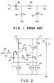
- FIG. 1 is a schematic circuit diagram an example of the configuration of a conventional bandpass filter.
- an input terminal 31 which accepts an input signal v i is connected to one end of a capacitor 32, which has a capacitance value of C31.
- the other end of the capacitor 32 is connected to one end of a resistor 33 which has a resistance value of R31, and also to one end of a resistor 34 which has a resistance value of R32.
- the other end of the resistor 33 is grounded.
- the other end of the resistor 34 is grounded through a capacitor 35 which has a capacitance value of C 32, and is also connected to an output terminal 36 used to output an output signal v o .
- the transfer function G(b/a) is given by equation (1).
- the cutoff frequency ⁇ 0 is expressed by equation (2).
- the quality factor Q and the peak gain H are expressed by equation (3) and equation (4), respectively.
- the quality factor Q cannot be set to a value of 0.5 or higher.
- Another shortcoming is that it is not possible to have a peak gain H of 1 or higher.
- Equation (4) can be rewritten in the form of equation (9). Since C31, C32, R31, and R32 are all larger than zero, it is impossible for the peak gain H to be 1 or higher. To achieve superior filter characteristics, it is desirable to have a waveform as the output signal v o that changes sharply with respect to frequency, that is, it is desirable that the value of Q be made large. Enabling the setting of the peak gain H to a value of 1 or higher is also advantageous from the standpoint of circuit design.
- Japanese laid-open patent No. 1989-067015 discloses a filter in that the values of quality factor Q and peak gain can be made larger than those of the conventional filter described above.
- This filter includes complicated transformer-conductance amplifiers (variable voltage-current converters).
- Japanese laid-open patent No. 1994-283965 discloses an active filter without variable voltage-current converters. This filter, however, is not an active bandpass filter but an active lowpass filter.
- the present invention has as an object the provision of an active bandpass filter of simple circuit configuration which offers free setting of the value of quality factor Q and peak gain.
- the present invention provides an active bandpass filter having an input terminal and an output terminal, comprising: a first transistor having an emitter, a base connected to an input terminal via a first resistance element, a collector connected both to a constant voltage source via a second resistance element and to the output terminal; first means for supplying a first constant current to the emitter of the first transistor; a second transistor having a base connected to the emitter of the first transistor via a third resistance element, a collector connected to the constant voltage source via a fourth resistance element and an emitter connected to the base of the first transistor via a first capacitance element; second means for supplying a second constant current to the emitter of the second transistor; a third transistor having a base connected to the collector of the second transistor, a collector connected to the constant voltage source and an emitter connected to the base of the second transistor via a second capacitance element; and third means for supplying a third constant current to the emitter of the third transistor.
- the first, second and third means may include a constant current source or a resistance element.
- FIG. 2 is a circuit diagram which shows the configuration of a preferred embodiment of an active bandpass filter according to the present invention.
- the base of a first bipolar transistor 11 is connected to an input terminal 24 via a first resistor 14 having a resistance value of R1.
- the collector of the transistor 11 is connected to a voltage regulator 20 for supplying a constant voltage V1 to the filter via a second resistor 15 having a resistance value of R2 and is also connected to an output terminal 25.
- the emitter of the transistor 11 is connected to a first constant current source 21 for supplying a first constant current I1 to the transistor 11.
- the base of a second bipolar transistor 12 is connected to the emitter of the transistor 11 via a third resistor 16 having a resistance value of R3.
- the collector of transistor 12 is connected to the voltage regulator 20 via a fourth resistor 17 having a resistance value of R4.
- the emitter of the transistor 12 is connected to the base of the transistor 11 via a first capacitor 18 having a capacitance value of C1 and is also connected to a second constant current source 22 for supplying a second constant current I2 to the transistor 12.
- the base of a third bipolar transistor 13 is connected to the collector of the transistor 12.
- the collector of the transistor 13 is connected to the voltage regulator 20.
- the emitter of the transistor 13 is connected to the base of the transistor 12 via a second capacitor 19 having a capacitance value of C2, and is also connected to a third constant current source 23 for supplying a third constant current I3 to the transistor 13.
- an input signal voltage V a at the input terminal 24, a base voltage V b of the transistor 11, a base voltage V c of the transistor 12, a base voltage V d of the transistor 13, and an output signal voltage V e at the output terminal 25 are expressed by equations (10) through (13). Additionally, by virtue of equations (10) through (13), the overall transfer function G(e/a) of the active bandpass filter is given by equation (14). The cutoff frequency ⁇ 0 is expressed by equation (15). The quality factor Q and peak gain H are given by equation (16) and equation (17), respectively.
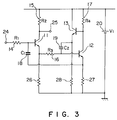
- FIG. 3 is a schematic circuit diagram which shows another preferred embodiment of an active bandpass filter according to the present invention.
- elements which are the same as shown in FIG. 2 are assigned the same reference numerals.
- the configuration differs from the configuration shown in FIG. 2 in that resistors 26, 27, and 28 are used instead of the first through third constant current sources 21, 22 and 23. Combination of resistors and constant current sources is also available, such as, the current sources 21 and 22 and the resistor 28.
- an active bandpass filter offering free setting of the values of quality factor Q and peak gain is provided.
Landscapes
- Networks Using Active Elements (AREA)
Applications Claiming Priority (2)
| Application Number | Priority Date | Filing Date | Title |
|---|---|---|---|
| JP6180309A JP3072002B2 (ja) | 1994-08-01 | 1994-08-01 | アクティブバンドパスフィルタ |
| JP180309/94 | 1994-08-01 |
Publications (2)
| Publication Number | Publication Date |
|---|---|
| EP0696104A1 true EP0696104A1 (fr) | 1996-02-07 |
| EP0696104B1 EP0696104B1 (fr) | 1999-03-31 |
Family
ID=16080965
Family Applications (1)
| Application Number | Title | Priority Date | Filing Date |
|---|---|---|---|
| EP95112084A Expired - Lifetime EP0696104B1 (fr) | 1994-08-01 | 1995-08-01 | Filtre passe-bande actif |
Country Status (6)
| Country | Link |
|---|---|
| US (1) | US5561394A (fr) |
| EP (1) | EP0696104B1 (fr) |
| JP (1) | JP3072002B2 (fr) |
| KR (1) | KR100201037B1 (fr) |
| CN (1) | CN1075686C (fr) |
| DE (1) | DE69508672T2 (fr) |
Cited By (2)
| Publication number | Priority date | Publication date | Assignee | Title |
|---|---|---|---|---|
| GB2329537A (en) * | 1997-09-12 | 1999-03-24 | Siemens Ag | Integrated low-pass filter |
| US9246453B2 (en) | 2007-09-20 | 2016-01-26 | Nxp, B.V. | Tunable RF filter |
Families Citing this family (4)
| Publication number | Priority date | Publication date | Assignee | Title |
|---|---|---|---|---|
| GB2295932B (en) * | 1994-12-08 | 1999-04-14 | Motorola Inc | Two-stage operational amplifier circuit |
| DK0772359T3 (da) * | 1995-10-31 | 2002-05-06 | Koninkl Philips Electronics Nv | Filtreringsindretning til behandling af en flerhed af kanaler i et kabelfjernsynsfordelingssystem |
| CN101877576B (zh) * | 2009-04-30 | 2012-10-03 | 华为技术有限公司 | 一种滤波电路以及具有该滤波电路的通信设备 |
| JP2014083210A (ja) * | 2012-10-23 | 2014-05-12 | Heiwa Mannequin Co Ltd | 表示器 |
Citations (4)
| Publication number | Priority date | Publication date | Assignee | Title |
|---|---|---|---|---|
| GB1603530A (en) * | 1977-07-18 | 1981-11-25 | Westinghouse Air Brake Co | Filtering circuit |
| EP0086026A2 (fr) * | 1982-02-10 | 1983-08-17 | Motorola, Inc. | Filtre intégré réjecteur de fréquence à bande étroite |
| JPS6467015A (en) | 1987-09-07 | 1989-03-13 | Toshiba Corp | Filter circuit |
| JPH06283965A (ja) | 1993-03-30 | 1994-10-07 | Toshiba Corp | アクティブ型ローパスフィルタ |
Family Cites Families (2)
| Publication number | Priority date | Publication date | Assignee | Title |
|---|---|---|---|---|
| JPS5732509B2 (fr) * | 1974-04-05 | 1982-07-12 | ||
| US3974399A (en) * | 1974-05-09 | 1976-08-10 | Yagi Antenna Co., Ltd. | Active high Q filter using transistor |
-
1994
- 1994-08-01 JP JP6180309A patent/JP3072002B2/ja not_active Expired - Fee Related
-
1995
- 1995-06-07 US US08/487,535 patent/US5561394A/en not_active Expired - Lifetime
- 1995-08-01 DE DE69508672T patent/DE69508672T2/de not_active Expired - Fee Related
- 1995-08-01 EP EP95112084A patent/EP0696104B1/fr not_active Expired - Lifetime
- 1995-08-01 CN CN95108681A patent/CN1075686C/zh not_active Expired - Fee Related
- 1995-08-01 KR KR1019950023642A patent/KR100201037B1/ko not_active Expired - Fee Related
Patent Citations (4)
| Publication number | Priority date | Publication date | Assignee | Title |
|---|---|---|---|---|
| GB1603530A (en) * | 1977-07-18 | 1981-11-25 | Westinghouse Air Brake Co | Filtering circuit |
| EP0086026A2 (fr) * | 1982-02-10 | 1983-08-17 | Motorola, Inc. | Filtre intégré réjecteur de fréquence à bande étroite |
| JPS6467015A (en) | 1987-09-07 | 1989-03-13 | Toshiba Corp | Filter circuit |
| JPH06283965A (ja) | 1993-03-30 | 1994-10-07 | Toshiba Corp | アクティブ型ローパスフィルタ |
Cited By (3)
| Publication number | Priority date | Publication date | Assignee | Title |
|---|---|---|---|---|
| GB2329537A (en) * | 1997-09-12 | 1999-03-24 | Siemens Ag | Integrated low-pass filter |
| GB2329537B (en) * | 1997-09-12 | 2001-09-26 | Siemens Ag | Integrated low-pass filter |
| US9246453B2 (en) | 2007-09-20 | 2016-01-26 | Nxp, B.V. | Tunable RF filter |
Also Published As
| Publication number | Publication date |
|---|---|
| KR960009384A (ko) | 1996-03-22 |
| CN1122971A (zh) | 1996-05-22 |
| CN1075686C (zh) | 2001-11-28 |
| US5561394A (en) | 1996-10-01 |
| DE69508672T2 (de) | 1999-09-09 |
| EP0696104B1 (fr) | 1999-03-31 |
| JP3072002B2 (ja) | 2000-07-31 |
| DE69508672D1 (de) | 1999-05-06 |
| KR100201037B1 (ko) | 1999-06-15 |
| JPH0846477A (ja) | 1996-02-16 |
Similar Documents
| Publication | Publication Date | Title |
|---|---|---|
| EP0435472B1 (fr) | Filtre actif | |
| EP0610066A1 (fr) | Multiplicateur de capacitance pour la compensation interne de fréquence de circuits intégrés régulateurs à découpage | |
| JPH0716142B2 (ja) | フィルター回路 | |
| EP0696104A1 (fr) | Filtre passe-bande actif | |
| JPS60254815A (ja) | フイルタ装置 | |
| US5574398A (en) | Active bandpass filter | |
| US4982422A (en) | Terminating circuit in a battery feed circuit of an electronic exchange system | |
| EP0049997A2 (fr) | Circuit de filtre apte à être construit comme circuit intégré | |
| EP0322379B1 (fr) | Filtre passe-bas actif intégré de premier degré | |
| JPH04148388A (ja) | 時定数可変形の微分器 | |
| US5229734A (en) | Filter with adjustable edge steepness | |
| EP0829959A2 (fr) | Circuit de filtrage | |
| US6529068B1 (en) | Area-efficient reconstruction filters, particularly for current-driven D/A converters | |
| EP0602723A1 (fr) | Circuit intégré comportant un paramètre ajustable électriquement | |
| EP0190469A1 (fr) | Amplificateur de transconductance | |
| JP3025718B2 (ja) | ラグリードフィルタ | |
| JPH06283965A (ja) | アクティブ型ローパスフィルタ | |
| SU1418679A2 (ru) | Импульсный стабилизатор посто нного тока | |
| JPH02309805A (ja) | 減衰回路 | |
| JP2730107B2 (ja) | カレントミラー回路 | |
| JPH08256040A (ja) | 容量装置およびそれを用いたフィルタ装置 | |
| JPH1079642A (ja) | フィルタ回路 | |
| SU1201820A1 (ru) | Стабилизатор двухпол рного напр жени | |
| GB2220092A (en) | Integrating circuit | |
| JPH0585083B2 (fr) |
Legal Events
| Date | Code | Title | Description |
|---|---|---|---|
| PUAI | Public reference made under article 153(3) epc to a published international application that has entered the european phase |
Free format text: ORIGINAL CODE: 0009012 |
|
| 17P | Request for examination filed |
Effective date: 19950801 |
|
| AK | Designated contracting states |
Kind code of ref document: A1 Designated state(s): DE FR GB |
|
| GRAG | Despatch of communication of intention to grant |
Free format text: ORIGINAL CODE: EPIDOS AGRA |
|
| 17Q | First examination report despatched |
Effective date: 19980703 |
|
| GRAG | Despatch of communication of intention to grant |
Free format text: ORIGINAL CODE: EPIDOS AGRA |
|
| GRAH | Despatch of communication of intention to grant a patent |
Free format text: ORIGINAL CODE: EPIDOS IGRA |
|
| GRAH | Despatch of communication of intention to grant a patent |
Free format text: ORIGINAL CODE: EPIDOS IGRA |
|
| GRAA | (expected) grant |
Free format text: ORIGINAL CODE: 0009210 |
|
| AK | Designated contracting states |
Kind code of ref document: B1 Designated state(s): DE FR GB |
|
| REF | Corresponds to: |
Ref document number: 69508672 Country of ref document: DE Date of ref document: 19990506 |
|
| ET | Fr: translation filed | ||
| PLBE | No opposition filed within time limit |
Free format text: ORIGINAL CODE: 0009261 |
|
| STAA | Information on the status of an ep patent application or granted ep patent |
Free format text: STATUS: NO OPPOSITION FILED WITHIN TIME LIMIT |
|
| 26N | No opposition filed | ||
| REG | Reference to a national code |
Ref country code: GB Ref legal event code: IF02 |
|
| PGFP | Annual fee paid to national office [announced via postgrant information from national office to epo] |
Ref country code: DE Payment date: 20080814 Year of fee payment: 14 |
|
| PGFP | Annual fee paid to national office [announced via postgrant information from national office to epo] |
Ref country code: FR Payment date: 20080818 Year of fee payment: 14 |
|
| PGFP | Annual fee paid to national office [announced via postgrant information from national office to epo] |
Ref country code: GB Payment date: 20080813 Year of fee payment: 14 |
|
| GBPC | Gb: european patent ceased through non-payment of renewal fee |
Effective date: 20090801 |
|
| REG | Reference to a national code |
Ref country code: FR Ref legal event code: ST Effective date: 20100430 |
|
| PG25 | Lapsed in a contracting state [announced via postgrant information from national office to epo] |
Ref country code: FR Free format text: LAPSE BECAUSE OF NON-PAYMENT OF DUE FEES Effective date: 20090831 Ref country code: DE Free format text: LAPSE BECAUSE OF NON-PAYMENT OF DUE FEES Effective date: 20100302 |
|
| PG25 | Lapsed in a contracting state [announced via postgrant information from national office to epo] |
Ref country code: GB Free format text: LAPSE BECAUSE OF NON-PAYMENT OF DUE FEES Effective date: 20090801 |