EP0696116A1 - Verfahren zum Abtasten eines digitalen Signals - Google Patents
Verfahren zum Abtasten eines digitalen Signals Download PDFInfo
- Publication number
- EP0696116A1 EP0696116A1 EP95401730A EP95401730A EP0696116A1 EP 0696116 A1 EP0696116 A1 EP 0696116A1 EP 95401730 A EP95401730 A EP 95401730A EP 95401730 A EP95401730 A EP 95401730A EP 0696116 A1 EP0696116 A1 EP 0696116A1
- Authority
- EP
- European Patent Office
- Prior art keywords
- sampling
- digital signal
- instants
- signal
- delay
- Prior art date
- Legal status (The legal status is an assumption and is not a legal conclusion. Google has not performed a legal analysis and makes no representation as to the accuracy of the status listed.)
- Granted
Links
Images


Classifications
-
- H—ELECTRICITY
- H04—ELECTRIC COMMUNICATION TECHNIQUE
- H04L—TRANSMISSION OF DIGITAL INFORMATION, e.g. TELEGRAPHIC COMMUNICATION
- H04L7/00—Arrangements for synchronising receiver with transmitter
- H04L7/02—Speed or phase control by the received code signals, the signals containing no special synchronisation information
- H04L7/033—Speed or phase control by the received code signals, the signals containing no special synchronisation information using the transitions of the received signal to control the phase of the synchronising-signal-generating means, e.g. using a phase-locked loop
- H04L7/0337—Selecting between two or more discretely delayed clocks or selecting between two or more discretely delayed received code signals
-
- H—ELECTRICITY
- H04—ELECTRIC COMMUNICATION TECHNIQUE
- H04L—TRANSMISSION OF DIGITAL INFORMATION, e.g. TELEGRAPHIC COMMUNICATION
- H04L7/00—Arrangements for synchronising receiver with transmitter
- H04L7/0016—Arrangements for synchronising receiver with transmitter correction of synchronization errors
- H04L7/002—Arrangements for synchronising receiver with transmitter correction of synchronization errors correction by interpolation
- H04L7/0029—Arrangements for synchronising receiver with transmitter correction of synchronization errors correction by interpolation interpolation of received data signal
Definitions
- the invention relates to methods for sampling a digital signal in series. It is more particularly suitable for high speed digital transmission, greater than one gigabit per second, and applies in particular to receivers of a digital serial transmission system, to computer systems, for example for the transmission of data between a processor and a memory or a cache memory, to long-distance telecommunications systems and private communication systems, such as local area networks and large networks (Wide Area Networks), as well as to data-processing systems.
- the subject of the invention is a method of sampling a signal in series, comprising beforehand the phase setting of the digital signal on a clock signal. Its corollary object is the integrated circuit and the system implementing this method.
- the documents EP-A-0441684, EP-A-0466591, EP-A-0466592 and EP-A-0466593 relate to a serial digital data transmission system.
- the first document describes a phase locked circuit and a frequency multiplier serving as a basis for the structure of the transmission system described in the other three documents.
- This system has essentially the double advantage of being particularly suitable for high speed digital transmission since it avoids the conventional use of a phase locked oscillator (VCO), and of having a simple structure for reliable operation.
- the second of the cited documents relates to a transmission method consisting in adding to the transmitted words (usually bytes) respective edges serving both as a synchronization signal and as a clock signal. In the receiver, these edges are used to reconstruct the clock signal which was used for transmission.
- the technique using these edges in the digital signal has the advantage of not imposing any constraint on the operating mode of the two remote stations which communicate by means of this signal via a serial link.
- Stations can work and transmit on the link at different frequencies.
- Multiprocessor computer systems can integrate processors from various origins and from different generations. In this case, this heterogeneity can be managed using this technique and protocols developed at a higher level.
- each station is sequenced by an internal clock of high precision and known frequency, fixed by the standard. The transmitter and the receiver therefore operate at this frequency. Under these conditions, the receiver knows the clock frequency which was used for transmission and no longer has to reconstruct the clock signal. The only task left to the receiver is to phase-phase the digital signal received on the internal clock signal.
- Edges are chosen as a reference in the received signal, for example the synchronization and clock edges in the receiver of the system described in the aforementioned documents, and are brought into phase with corresponding edges of the clock signal.
- the receiver performs the sampling of the digital signal after a predetermined delay with respect to the reference edges. Sampling takes place in a zone of maximum signal stability following each reference edge so as to have an optimal determination of the logical value of each bit.
- R the recurrence period of the bits transmitted in series by means of the digital signal
- the delay between an edge of the received signal and the best sampling instant is usually equal to R / 2 or R / 2 + nR where n is a positive integer.
- This conventional sampling method has several drawbacks.
- clocks have a very precise frequency to ensure a perfect correspondence between the clock which was used for transmission and the clock which is used for reception.
- clocks are usually made from quartz, which exhibit certain technological dispersions and certain drifts depending on the conditions of use (temperature, etc.).
- a difference between the transmit and receive clocks accumulates and disturbs the phase timing.
- the signal undergoes a delay which depends on the length of the transmission line. This length is usually very variable and unknown.
- the timing in phase must therefore be very effective. Sampling can therefore occur outside a stability zone of the received signal and thus provide a false value of the bits read.
- a clock accuracy of the order of 10 ⁇ 6 is currently required.
- the invention aims to remedy the shortcomings of conventional sampling and to adapt the transmission system described in the aforementioned documents to market standards, in order to associate the advantages of this system with those of standards.
- the subject of the invention is a sampling method which can tolerate less precision of the clocks while allowing simple, effective phase calibration and ensuring reliable reconstruction of the data received.
- the subject of the invention is a method for sampling a digital signal in series, comprising a phase setting of the digital signal on a clock signal and a sampling of the digital signal at delayed times, characterized in that that the phase setting is made with reference to the sampling instants.
- the invention also relates to a digital serial transmission system implementing the method of the invention and an integrated circuit incorporating a digital receiver in series implementing the method.
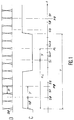
- FIG. 1 schematically represents a digital data signal in series D and a clock signal C.
- FIG. 1 also represents the sampling instants S0-S9 recurrent at the period R of ten successive bits of the data signal so as to determine the logic value thereof.
- the ten sampling instants Si (S0-S9) refer to the same edge of the clock signal C in period T, the rising edge in FIG. 1, and are determined with respect to this edge by ten respective delays Xi (X0-X9).
- the delays Xi are variable values around a mean value verifying the previous relationship.
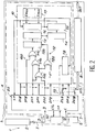
- FIG. 2 illustrates in block diagram a digital serial transmission system 1 comprising a transmitter 2 connected via a serial transmission line 3 to a receiver 4.
- the receiver 4 is incorporated in an integrated circuit 5 and comprises a clock 6 generating the clock signal C, setting and sampling means 7 receiving the clock signal C and the digital signal D, and an output circuit 8 shaping the digital signal sampled so that the signal output signal from the receiver corresponds to the digital signal applied to the transmitter.
- the calibration and sampling means 7 comprise a calibration test circuit 10 and a sampling circuit 20 which implement the method which has just been described with reference to FIG. 1.
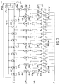
- FIG. 3 illustrates a first example of a sampling circuit 20 according to the invention, based on the structure used in the aforementioned documents to obtain all the advantages thereof.
- Circuit 20 is a phase locked circuit comprising: four inputs for, respectively, the clock signal C, the digital signal D, a control signal XP from the timing test circuit 10 and a control signal YP from 'a circuit 30; a phase comparator 21 having a first input 21a directly receiving the clock signal, a second input receiving the clock signal C via a first group, ten in the example illustrated, of delay elements 22 connected in cascade and each provided with a control terminal to adjust the delay, and an output providing a phase error signal which can be made for example of two respective increment (+) and decrement (- ) or of a single binary signal, the two states of which have the respective functions of incrementation and decrementation; and a digital control device such as an up-down counter 23 having an input receiving the phase error signal from the phase comparator and supplying a digital control signal CTL to the respective
- the ten output signals Ci (C0-C9) of the delay elements 22 are applied to the respective inputs of a second group of ten delay elements 24 whose respective delays are set to a same value X by the control signal XP.
- the output signals Si (S0-S9) of the delay elements 24 are applied to the respective control terminals of ten sampling flip-flops 25 sampling the digital signal D at the instants Si to supply the desired sampling signals DSi (DS0-DS9) representative of the logical values of ten successive bits of signal D.
- the set DS of sampling signals DSi is applied to the input of the output circuit 8, as shown in the figure 2.
- the output signals Si (S0-S9) of the delay elements 24 are also applied to the respective inputs of a third group of ten delay elements 26 whose respective delays are set to the same value Y by the control signal YP.
- the output signals Pi (P0-P9) of the delay elements 26 are applied to the respective control terminals of ten test flip-flops 27 sampling the digital signal D at the instants Pi to provide the corresponding test samples DPi (DP0-DP9).
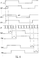
- the delays Xi (X0-X9) which refer in FIG. 1 to the rising edge of the clock signal C are determined from ten auxiliary clock signals Ci (C0-C9) originating from the clock signal C by the equal and successive delays of the delay elements 22 (see FIG. 4).
- the period T of the clock signal is divided into ten equal delays which, when the digital signal D is exactly set to the clock signal C, correspond to the recurrence period R of the bits of the digital signal D, as shown in FIGS. 3 and 4.
- the transitions of the digital signal D are ahead of the rising edges of the clock signal C by the same value since the timing is assumed to be perfect.
- the duration 3R / 2 is therefore an average value of X.
- the samples DPi and DSi obtained from the digital signal D at the respective times Pi and Si are supplied as input signals to the timing test circuit 10.
- FIG. 5 illustrates one of the possible variants of the sampling circuit 20.
- the components common to the circuits 20 of FIGS. 3 and 5 are designated by the same reference numbers.
- the group of delay elements 24 in FIG. 2 is reduced to a single element 24 and the group of delay elements 22 in FIG. 3 is split into two groups 22 and 22 ′ connected in series via the element 24 and controlled by the output signal CTL of the up-down counter 23.
- the delay elements 22 are connected between the input terminal of the clock signal C and an input of the phase comparator 21 while the delay elements 22 'provide at their respective inputs the signals S0-S9 applied to the delay elements 26 and to the sampling flip-flops 25 and 27.
- the last element of the group 22' could be eliminated but it constitutes a load similar to the other elements and contributes to obtaining equal delays between signals S0-S9.
- FIG. 2 illustrates the structure of the timing test circuit 10.
- each cell 10i of the circuit 10 comprises three logic OR-Exclusive gates (XOR gates) 11a, 11b and 11c with two inputs.
- the gate 11a receives the bit samples DSi + 1 and DSi + 2 (DS1 and DS2 in the cell 100) and checks the value of Si + 1 ⁇ If + 2.
- the second gate 11b receives the sample DSi + 1 (DS 1) and the result provided by the gate 11a to check whether the edge is rising or falling.
- DSi + 2 1
- the output of gate 11b has the value 1 indicating a rising edge.
- the selection device 12 comprises a door XOR 12a having an input connected to the output of the door 11a and a second input receiving the logic value 1, and a holding circuit (a flip-flop, for example) 12b having a control terminal connected to the output of the door 12a, an input connected to the output of the door 11c, and output. If an edge is detected by gate 11a, the output of gate 12a has the value 0 and commands the holding circuit 12b to provide an equal or inverse output to its input.
- the output of the gate 12a has the logic value 1 and controls the holding circuit 12b to keep the input value at the output. Under these conditions, the output of the holding circuit 12b is only representative of a phase advance or delay when a transition is detected.
- the result provided by all the flip-flops 12b of cells 10i of circuit 10 can be used as a control signal XP to adjust the delays X of FIG. 3 or Xi in FIG. 1.
- the detection of a phase advance then increases the delay Xi and a phase delay decreases it.
- the circuit 10 of the example illustrated can only detect a phase advance and a delay, so that a perfect phase setting results in a succession of alternating advances and delays. Consequently, the direct adjustment of the delays X would result in an oscillation state of the circuit 10 and would produce an instability of the adjustment loop. In order to avoid this state, the adjustment of the delays X is controlled after a delay of the results provided by the flip-flop 12b.
- this time delay is made by counting bits 1 and 0 obtained at the output of the flip-flop 12b in a predetermined duration, 4T for example.
- the circuit 10 therefore comprises an up-down counter 13 connected to the output of the flip-flop 12b for for example adding the bits 1 and subtracting the bits 0 for four periods T from the clock signal C and supplying the sampling control signal XP to the sampling circuit 20 to adjust the delays X.
- the output of the up-down counter 13 is connected to a threshold device 14 provided for trigger a second up-down counter 15 so as to activate the setting only if the counting result exceeds a predetermined value.
- FIG. 6 illustrates an example of generation of the control signal YP of the delays Y in the sampling circuit 20.
- the control signal YP is produced by a control circuit 30 represented in the form of a block in FIG. 2 and in schematic form in FIG. 6.
- the control circuit 30 comprises: an input terminal for the clock signal C and an input terminal for the control signal CTL produced by the up-down counter 23 of the sampling circuit 20; a phase comparator 31 with two inputs; a first branch made of an odd number 21 + 1 of delay elements 32, three in the example illustrated, each effecting a delay of the bit period R, controlled by the signal CTL and connected in cascade between the terminal d input of the clock signal C and an input of the phase comparator 31; and a second branch made of an even number 2m of delay elements 33, two in the example illustrated, each effecting a delay Y, connected in cascade between the input terminal of the clock signal C and the other input of the phase comparator 31, controlled by the output of the phase comparator and supplying the adjustment signal YP
- the invention therefore offers the advantage of reacting the phase timing and the sampling on each other.
- the resulting adjustment is therefore much more effective than that which can be obtained from the prior art and allows, for the same bit rate, to tolerate greater margins in the precision of the clocks between transmitters and receivers.
- the system can compensate for variations in clock frequency 50 ps (picoseconds ) every 40 ns (nanoseconds), that is to say variations of the order of 10 ⁇ 3, which are approximately a thousand times greater than those which can be compensated in the prior art.
- the system is less influenced by technological dispersions and functional drifts. But it also means that the method of the invention is very suitable for higher flow rates without being subject to constraints in the precision of the clocks.
- the invention can be applied in very diverse transmission systems, it is particularly well suited to the system described in the aforementioned documents.
- delay X has a limited range of variation to ensure efficient and reliable sampling.
- the digital signal D is perfectly calibrated on the clock signal C, that the delays X are then all equal and that their value depends on the advance or the delay between the two signals C and D.
- the value X is less than 3R / 2 to take account of the phase advance of the signal D.
- the digital signal D has a succession of periods equal to R - ⁇ R, i.e. slightly shorter by the same value ⁇ R as the period R supplied by the auxiliary clock signals C0-C9 of the clock signal C, the advance that the signal D on the signal C in FIG.
- Xmin can have a zero value, but the realization of very short adjustable delays poses many problems which make that the chosen average value of X is 3R / 2, and not R / 2 if the frequency of the signal D is very high, for example of the order of a gigahertz. If X becomes negative, this means that the clock is too slow and that a bit of the digital signal D cannot be sampled. Conversely, a gradual increase in the period R would increase the value of X up to a theoretical value of 5R / 2, beyond which the sampling circuit 20 would read the same bit twice.
- the invention also offers the advantage of compensating for the extraperiodic drifts between the two signals D and C. Compensation consists in adding or subtracting a recurrence period R according to whether the clock is too fast or too slow compared to the period of recurrence of the bits of the digital signal D, so that the variation of the value of X remains included in a period of recurrence R while allowing the detection and the correct restitution of all the bits of the digital signal D. According to the example illustrated in FIG.
- the compensation means include in the timing test circuit 10 a period switch 16 receiving the adjustment signal XP and supplying a control signal to an input of the second up-down counter 15.
- FIG. 7 represents an exemplary embodiment of the control circuit 17, comprising: two input terminals for the clock signal C and the control signal CTL coming from the sampling circuit 20; a block providing a signal representative of the minimum value Xmin of X; and a phase comparator 41 with two inputs connected by two respective branches to the clock signal C, the first branch comprising a delay element 42 representative of the period R and consequently controlled by the signal CTL and a delay element 43 producing a delay having the value Xmin which is supplied to it, and the second branch comprising only a delay element delay 44 controlled by the phase error signal leaving the phase comparator 41.
- the balance of the two branches therefore leads the delay element 44 to have the value Xmax. It is clear that the value Xmax could be chosen as a reference, so that the control circuit 17 would then supply the value Xmin.
- the period switch 16 performs a shift of a recurrence period R of the bits, in advance or in phase delay if the delay XP becomes respectively less than Xmin or greater than Xmax.
- FIG. 8 is a timing diagram illustrating the clock signal C and the ten sampling signals Si (S0-S9) of FIG. 4.
- a signal S10 is added, represented by a broken line in FIG. 8, delayed by the period R relative to the signal S9.
- FIGS. 2 and 3 An exemplary embodiment of the invention is given in FIGS. 2 and 3.
- the additional sampling signal S10 is obtained, like the signals Si, from an additional delay element 22 receiving the signal C9 and controlled by the signal CTL and a second delay element 24 receiving the output signal from the first delay element 22 and controlled by the signal XP.
- the signal S10 leaving the element 24 controls an additional sampling flip-flop 25 receiving the signal D and providing the sample DS10.
- the output signal from the switch 16 is also applied to a multiplexer 18.
- the function of the multiplexer 18 is symbolized by the switch 19 indicated in FIG. 2.
- the switch 19 makes it possible to disconnect the signal S9 or to add signal S10.
- the delimitation of the words for reconstructing the transmitted data signal does not pose any particular problem.
- the words are separated from one another by a synchronization and clock transition which serves to delimit them.
- Conventional codes define a sequence of word reconstruction, usually a series of bits that can never be found in normal transmission, which the transmitter sends cyclically.
- the receiver determines the position of the words in the data received in series and counts the bits to form the words.
- the receiver determines the position of the words in the data received in series and counts the bits to form the words.
- the method which has just been described has the fundamental characteristic of referring to the sampling instants Si to make the phase setting.
- the presently preferred form of the invention for making this calibration consists in determining instants of phase calibration test Pi referring to the sampling instants Si in order to verify whether the transitions of the digital signal are ahead or behind in phase with respect to at the timing test instants If.
- this form is not necessary, other shapes being able to avoid the determination of timing test instants, for example by producing a reference signal referring to sampling times. and to compare this signal with the digital signal D.
- a complementary delay Y kR / 2 where k is an integer non-zero positive odd and R denotes the period of recurrence of the bits of the digital signal D.
- the signals Si are obtained from auxiliary clock signals Ci and it is understood that other forms of obtaining are possible.
- the timing test consists in detecting the presence and the direction of a transition of the digital signal and in checking whether the value of the digital signal analyzed at the test instant is that corresponding to an advance or a delay of phase with respect to the detected transition.
- Many variants are within the reach of those skilled in the art. For example, instead of doing it on all transitions, only some can be chosen, for example rising transitions and / or one transition in four.
- the timing test can be independent of the direction.
- the method consists in assigning limit values to the delays X of the sampling instants and, when these limit values are exceeded, shifting the sampling of the digital signal by a period R of recurrence of the bits of this signal and compensating for the shift so as to restore all the bits of the digital signal.
- compensation is made by selective addition of an additional sampling signal S10 or by selective suppression of the first or last sampling signal S0 or S9.
- the corollary object of the invention is therefore a digital transmission system in series 1 comprising a transmitter 2 connected by a transmission link 3 of a digital signal in series D to a receiver 4 referring to a internal clock 6 delivering a clock signal C and setting and sampling means 7 implementing the method of the invention.
- the internal clock can be external to the receiver.
- the calibration and sampling means 7 comprising a calibration test circuit 10, where the doors 11a and 11b and the selection device 12 form detection means of a transition of the digital signal D, the sampling circuit 20 forms means receiving the clock signal C for the generation of a predetermined timing test, the gate 11c forms phase comparison means connected to the means detection 11a, 11b, 12 and of generation 20 to determine the phase difference between the timing test Pi and the transition, and the up-down counter 13 and the threshold device 14 connected to the output of the comparison means 11c form means for controlling the generation means 20 so as to tend towards phase matching between the digital signal D and the clock signal C.
- the detection of a transition can be accompanied by the detection of the direction of the transition.
- the generation means 20 comprise a phase locked circuit composed of a phase comparator 21 with two inputs receiving respectively the direct clock signal and the signal of the clock delayed by a first group of delay elements 22 in cascade representative of the recurrence period R of the bits of the digital signal D, a second group of delay elements 24 representative of the delays X of the sampling instants and a third group of delay elements 26 representative of the delays Y of the setting instants, the respective delay elements of the first, second and third groups being connected in series.
- the generation means 20 comprise a phase locked circuit composed of a phase comparator 21 with two inputs receiving respectively the direct clock signal and the clock signal delayed by a first group delay elements 22 in cascade representative of the recurrence period R of the bits of the digital signal D, an additional delay element 24 representative of the delay X of the sampling instants, receiving the clock signal and connected in series with a second group of delay elements 22 ′ representative of the recurrence period R of the bits of the digital signal D and connected in cascade, and a third group of delay elements 26 representative of the delays Y of the setting times and connected to the respective outputs of the additional delay element and delay elements of the second group.
- the setting and sampling means 7 also comprise means for determining limit values for the delay of the sampling instants, means for shifting the sampling instants of a period R if the delay of the sampling instants reaches one of the limit values and means for compensating the offset for the restitution of all the bits. Compensation includes the addition of a sampling signal. Deletion of a sampling signal is not necessary, since double sampling could occur and be taken into account for the correct reproduction of the output signal.
- the invention also has as a corollary object an integrated circuit 5 incorporating a receiver 4 of a digital signal in series D, the receiver comprising means for setting and sampling 7 of the digital signal which implement the method defined above and / or are made as indicated with reference to the transmission system.
Landscapes
- Engineering & Computer Science (AREA)
- Computer Networks & Wireless Communication (AREA)
- Signal Processing (AREA)
- Synchronisation In Digital Transmission Systems (AREA)
- Ultra Sonic Daignosis Equipment (AREA)
Applications Claiming Priority (2)
| Application Number | Priority Date | Filing Date | Title |
|---|---|---|---|
| FR9409683 | 1994-08-04 | ||
| FR9409683A FR2723494B1 (fr) | 1994-08-04 | 1994-08-04 | Procede d'echantillonnage d'un signal numerique en serie |
Publications (2)
| Publication Number | Publication Date |
|---|---|
| EP0696116A1 true EP0696116A1 (de) | 1996-02-07 |
| EP0696116B1 EP0696116B1 (de) | 2003-09-24 |
Family
ID=9466079
Family Applications (1)
| Application Number | Title | Priority Date | Filing Date |
|---|---|---|---|
| EP95401730A Expired - Lifetime EP0696116B1 (de) | 1994-08-04 | 1995-07-21 | Verfahren zum Abtasten eines seriellen digitalen Signals |
Country Status (6)
| Country | Link |
|---|---|
| US (1) | US5848109A (de) |
| EP (1) | EP0696116B1 (de) |
| JP (1) | JP2848800B2 (de) |
| CA (1) | CA2154545A1 (de) |
| DE (1) | DE69531810T2 (de) |
| FR (1) | FR2723494B1 (de) |
Families Citing this family (8)
| Publication number | Priority date | Publication date | Assignee | Title |
|---|---|---|---|---|
| US5978379A (en) | 1997-01-23 | 1999-11-02 | Gadzoox Networks, Inc. | Fiber channel learning bridge, learning half bridge, and protocol |
| US7430171B2 (en) | 1998-11-19 | 2008-09-30 | Broadcom Corporation | Fibre channel arbitrated loop bufferless switch circuitry to increase bandwidth without significant increase in cost |
| US6467043B1 (en) * | 1999-07-29 | 2002-10-15 | Micron Technology, Inc. | Adjusting and measuring the timing of a data strobe signal with a first delay line and through additional delay line adapted to receive pulse signal |
| DE60139121D1 (de) | 2000-04-28 | 2009-08-13 | Broadcom Corp | Sende- und empfangssysteme und zugehörige verfahren für serielle hochgeschwindigkeitsdaten |
| JP2003218847A (ja) * | 2002-01-28 | 2003-07-31 | Nec Corp | データ受信方式 |
| CN100379233C (zh) * | 2004-09-03 | 2008-04-02 | 杭州国芯科技有限公司 | 改进定时锁定检测的方法 |
| US7450039B2 (en) | 2006-07-05 | 2008-11-11 | Silicon Library Inc. | Transmission device and electronic apparatus with self-diagnostic function, and self-diagnostic method for use therein |
| US10367667B2 (en) * | 2017-09-29 | 2019-07-30 | Nxp B.V. | Joint ad-hoc signal and collision detection method |
Citations (7)
| Publication number | Priority date | Publication date | Assignee | Title |
|---|---|---|---|---|
| JPS58204651A (ja) * | 1982-05-24 | 1983-11-29 | Nec Corp | クロツク再生回路 |
| JPH01223887A (ja) * | 1988-03-03 | 1989-09-06 | Matsushita Electric Ind Co Ltd | ディスクおよびその記録装置およびその再生装置 |
| US5001729A (en) * | 1987-05-26 | 1991-03-19 | Hayes Microcomputer Products, Inc. | High speed half duplex modem with fast turnaround protocol |
| EP0441684A1 (de) | 1990-02-06 | 1991-08-14 | Bull S.A. | Phasenregelschaltung und dadurch entstandener Frequenzvervielfacher |
| EP0466591A1 (de) | 1990-07-11 | 1992-01-15 | Bull S.A. | Verfahren und Anordnung für digitale serielle Datenübertragung |
| EP0466593A1 (de) | 1990-07-11 | 1992-01-15 | Bull S.A. | Datenabtastschaltung und ein digitales Datenübertragungssystem dazu |
| EP0466592A1 (de) | 1990-07-11 | 1992-01-15 | Bull S.A. | Vorrichtung zu Parallelserien und zur Serienparallelwandlung von Daten und dadurch entstandenes serielles digitales Nachrichtenübertragungssystem |
Family Cites Families (4)
| Publication number | Priority date | Publication date | Assignee | Title |
|---|---|---|---|---|
| FR2309089A1 (fr) * | 1975-04-25 | 1976-11-19 | Ibm France | Procede pour synchroniser l'horloge du recepteur d'un systeme de transmission de donnees et dispositif pour mettre en oeuvre le procede |
| DE2632165B2 (de) * | 1976-07-16 | 1978-06-01 | Siemens Ag, 1000 Berlin Und 8000 Muenchen | Schaltungsanordnung zum Regeln der Folgefrequenz von Taktimpulsen |
| US4881059A (en) * | 1987-04-30 | 1989-11-14 | American Telephone And Telegraph Company | Manchester code receiver |
| US4972443A (en) * | 1987-11-24 | 1990-11-20 | Siemens Aktiengesellschaft | Method and arrangement for generating a correction signal for a digital clock recovery means |
-
1994
- 1994-08-04 FR FR9409683A patent/FR2723494B1/fr not_active Expired - Fee Related
-
1995
- 1995-07-21 DE DE69531810T patent/DE69531810T2/de not_active Expired - Lifetime
- 1995-07-21 EP EP95401730A patent/EP0696116B1/de not_active Expired - Lifetime
- 1995-07-24 CA CA002154545A patent/CA2154545A1/fr not_active Abandoned
- 1995-08-01 JP JP19673995A patent/JP2848800B2/ja not_active Expired - Lifetime
- 1995-08-02 US US08/510,458 patent/US5848109A/en not_active Expired - Lifetime
Patent Citations (7)
| Publication number | Priority date | Publication date | Assignee | Title |
|---|---|---|---|---|
| JPS58204651A (ja) * | 1982-05-24 | 1983-11-29 | Nec Corp | クロツク再生回路 |
| US5001729A (en) * | 1987-05-26 | 1991-03-19 | Hayes Microcomputer Products, Inc. | High speed half duplex modem with fast turnaround protocol |
| JPH01223887A (ja) * | 1988-03-03 | 1989-09-06 | Matsushita Electric Ind Co Ltd | ディスクおよびその記録装置およびその再生装置 |
| EP0441684A1 (de) | 1990-02-06 | 1991-08-14 | Bull S.A. | Phasenregelschaltung und dadurch entstandener Frequenzvervielfacher |
| EP0466591A1 (de) | 1990-07-11 | 1992-01-15 | Bull S.A. | Verfahren und Anordnung für digitale serielle Datenübertragung |
| EP0466593A1 (de) | 1990-07-11 | 1992-01-15 | Bull S.A. | Datenabtastschaltung und ein digitales Datenübertragungssystem dazu |
| EP0466592A1 (de) | 1990-07-11 | 1992-01-15 | Bull S.A. | Vorrichtung zu Parallelserien und zur Serienparallelwandlung von Daten und dadurch entstandenes serielles digitales Nachrichtenübertragungssystem |
Non-Patent Citations (2)
| Title |
|---|
| PATENT ABSTRACTS OF JAPAN vol. 13, no. 544 (E - 855) 6 December 1989 (1989-12-06) * |
| PATENT ABSTRACTS OF JAPAN vol. 8, no. 49 (E - 230) 6 March 1984 (1984-03-06) * |
Also Published As
| Publication number | Publication date |
|---|---|
| US5848109A (en) | 1998-12-08 |
| DE69531810T2 (de) | 2004-07-15 |
| CA2154545A1 (fr) | 1996-02-05 |
| EP0696116B1 (de) | 2003-09-24 |
| DE69531810D1 (de) | 2003-10-30 |
| FR2723494A1 (fr) | 1996-02-09 |
| FR2723494B1 (fr) | 1996-09-06 |
| JPH0888624A (ja) | 1996-04-02 |
| JP2848800B2 (ja) | 1999-01-20 |
Similar Documents
| Publication | Publication Date | Title |
|---|---|---|
| JP4064630B2 (ja) | スキューの影響を受けない低電圧差動受信器 | |
| EP0466591B1 (de) | Verfahren und Anordnung für digitale serielle Datenübertragung | |
| EP2137873B1 (de) | Vorrichtung zur rückgewinnung des taktsignales zur digitalen regelung der phase ohne externe regelung | |
| US6538475B1 (en) | Phase detector | |
| US7869544B2 (en) | System for measuring an eyewidth of a data signal in an asynchronous system | |
| FR2590425A1 (fr) | Appareillage pour regler les phases de signaux de donnees appliques a un circuit d'utilisation de donnees | |
| US7602869B2 (en) | Methods and apparatus for clock synchronization and data recovery in a receiver | |
| EP0645888A1 (de) | Digitale Verzögerungsleitung | |
| EP0696116B1 (de) | Verfahren zum Abtasten eines seriellen digitalen Signals | |
| EP0716501B1 (de) | Phasenvergleicher für ein digitales Signal und ein Taktsignal, und entsprechender Phasenregelkreis | |
| WO2017080925A1 (fr) | Procede de synchronisation de convertisseurs de donnees par un signal transmis de proche en proche | |
| EP0466593B1 (de) | Datenabtastschaltung und ein digitales Datenübertragungssystem dazu | |
| JP3109587B2 (ja) | オーバーサンプリング型クロックリカバリ回路 | |
| EP0396461B1 (de) | Anordnung zur Synchronisation eines pseudobinären Signals mit einem durch Phasensprung regenerierten Taktsignal | |
| JP3278621B2 (ja) | データ伝送装置 | |
| CN110557195B (zh) | 一种基于相干光通信的定时误差检测方法及装置 | |
| EP0526359B1 (de) | Verfahren und Schaltungsanordnung zur Synchronisierung eines Signals | |
| EP0689315B1 (de) | Phasenkomparator | |
| FR2770704A1 (fr) | Circuit verrouille en phase | |
| EP0373067B1 (de) | Sende-Empfangssynchronisationsvorrichtung einer Station eines Kommunikationsnetzes, insbesondere für ein Kraftfahrzeug | |
| EP0174880B1 (de) | Schaltungsanordnung zum Feststellen der Übergänge eines Datensignals in Bezug auf ein Taktsignal und diese Anordnung enthaltende Synchronisationseinrichtung | |
| EP3716523A1 (de) | Synchronisierungsverfahren von in serie gesendeten digitalen daten | |
| EP2143231B1 (de) | Vorrichtung zur rückgewinnung des taktes und digitaler daten ohne extenre regelung | |
| EP1131915B1 (de) | Ein verfahren und eine schaltung zur wiedergewinnung eines digitalen signales und taktes aus einem empfangenen datensignal | |
| FR2785751A1 (fr) | Procede de synchronisation d'une horloge locale d'un appareil sur l'horloge d'un reseau de communication sans fil et dispositif de synchronisation associe |
Legal Events
| Date | Code | Title | Description |
|---|---|---|---|
| PUAI | Public reference made under article 153(3) epc to a published international application that has entered the european phase |
Free format text: ORIGINAL CODE: 0009012 |
|
| AK | Designated contracting states |
Kind code of ref document: A1 Designated state(s): BE CH DE ES FR GB IT LI NL SE |
|
| 17P | Request for examination filed |
Effective date: 19960807 |
|
| 17Q | First examination report despatched |
Effective date: 20000920 |
|
| RTI1 | Title (correction) |
Free format text: METHOD FOR SAMPLING A SERIAL DIGITAL SIGNAL |
|
| GRAH | Despatch of communication of intention to grant a patent |
Free format text: ORIGINAL CODE: EPIDOS IGRA |
|
| GRAS | Grant fee paid |
Free format text: ORIGINAL CODE: EPIDOSNIGR3 |
|
| GRAA | (expected) grant |
Free format text: ORIGINAL CODE: 0009210 |
|
| AK | Designated contracting states |
Kind code of ref document: B1 Designated state(s): BE CH DE ES FR GB IT LI NL SE |
|
| PG25 | Lapsed in a contracting state [announced via postgrant information from national office to epo] |
Ref country code: NL Free format text: LAPSE BECAUSE OF FAILURE TO SUBMIT A TRANSLATION OF THE DESCRIPTION OR TO PAY THE FEE WITHIN THE PRESCRIBED TIME-LIMIT Effective date: 20030924 Ref country code: ES Free format text: LAPSE BECAUSE OF FAILURE TO SUBMIT A TRANSLATION OF THE DESCRIPTION OR TO PAY THE FEE WITHIN THE PRESCRIBED TIME-LIMIT Effective date: 20030924 |
|
| REG | Reference to a national code |
Ref country code: GB Ref legal event code: FG4D Free format text: NOT ENGLISH |
|
| REG | Reference to a national code |
Ref country code: CH Ref legal event code: EP |
|
| GBT | Gb: translation of ep patent filed (gb section 77(6)(a)/1977) | ||
| REF | Corresponds to: |
Ref document number: 69531810 Country of ref document: DE Date of ref document: 20031030 Kind code of ref document: P |
|
| PG25 | Lapsed in a contracting state [announced via postgrant information from national office to epo] |
Ref country code: SE Free format text: LAPSE BECAUSE OF FAILURE TO SUBMIT A TRANSLATION OF THE DESCRIPTION OR TO PAY THE FEE WITHIN THE PRESCRIBED TIME-LIMIT Effective date: 20031224 |
|
| NLV1 | Nl: lapsed or annulled due to failure to fulfill the requirements of art. 29p and 29m of the patents act | ||
| PLBE | No opposition filed within time limit |
Free format text: ORIGINAL CODE: 0009261 |
|
| STAA | Information on the status of an ep patent application or granted ep patent |
Free format text: STATUS: NO OPPOSITION FILED WITHIN TIME LIMIT |
|
| PG25 | Lapsed in a contracting state [announced via postgrant information from national office to epo] |
Ref country code: LI Free format text: LAPSE BECAUSE OF NON-PAYMENT OF DUE FEES Effective date: 20040731 Ref country code: CH Free format text: LAPSE BECAUSE OF NON-PAYMENT OF DUE FEES Effective date: 20040731 Ref country code: BE Free format text: LAPSE BECAUSE OF NON-PAYMENT OF DUE FEES Effective date: 20040731 |
|
| 26N | No opposition filed |
Effective date: 20040625 |
|
| BERE | Be: lapsed |
Owner name: S.A. *BULL Effective date: 20040731 |
|
| REG | Reference to a national code |
Ref country code: CH Ref legal event code: PL |
|
| BERE | Be: lapsed |
Owner name: S.A. *BULL Effective date: 20040731 |
|
| PGFP | Annual fee paid to national office [announced via postgrant information from national office to epo] |
Ref country code: GB Payment date: 20140624 Year of fee payment: 20 |
|
| PGFP | Annual fee paid to national office [announced via postgrant information from national office to epo] |
Ref country code: IT Payment date: 20140624 Year of fee payment: 20 |
|
| PGFP | Annual fee paid to national office [announced via postgrant information from national office to epo] |
Ref country code: DE Payment date: 20140620 Year of fee payment: 20 |
|
| PGFP | Annual fee paid to national office [announced via postgrant information from national office to epo] |
Ref country code: FR Payment date: 20140721 Year of fee payment: 20 |
|
| REG | Reference to a national code |
Ref country code: DE Ref legal event code: R071 Ref document number: 69531810 Country of ref document: DE |
|
| REG | Reference to a national code |
Ref country code: GB Ref legal event code: PE20 Expiry date: 20150720 |
|
| PG25 | Lapsed in a contracting state [announced via postgrant information from national office to epo] |
Ref country code: GB Free format text: LAPSE BECAUSE OF EXPIRATION OF PROTECTION Effective date: 20150720 |