EP0696743A2 - Méthode et dispositif auxiliaire pour l'accord d'une bobine de détection RMN - Google Patents
Méthode et dispositif auxiliaire pour l'accord d'une bobine de détection RMN Download PDFInfo
- Publication number
- EP0696743A2 EP0696743A2 EP95108822A EP95108822A EP0696743A2 EP 0696743 A2 EP0696743 A2 EP 0696743A2 EP 95108822 A EP95108822 A EP 95108822A EP 95108822 A EP95108822 A EP 95108822A EP 0696743 A2 EP0696743 A2 EP 0696743A2
- Authority
- EP
- European Patent Office
- Prior art keywords
- impedance
- signal
- tuning
- nmr
- path
- Prior art date
- Legal status (The legal status is an assumption and is not a legal conclusion. Google has not performed a legal analysis and makes no representation as to the accuracy of the status listed.)
- Granted
Links
Images


Classifications
-
- G—PHYSICS
- G01—MEASURING; TESTING
- G01R—MEASURING ELECTRIC VARIABLES; MEASURING MAGNETIC VARIABLES
- G01R33/00—Arrangements or instruments for measuring magnetic variables
- G01R33/20—Arrangements or instruments for measuring magnetic variables involving magnetic resonance
- G01R33/28—Details of apparatus provided for in groups G01R33/44 - G01R33/64
- G01R33/32—Excitation or detection systems, e.g. using radio frequency signals
- G01R33/36—Electrical details, e.g. matching or coupling of the coil to the receiver
- G01R33/3628—Tuning/matching of the transmit/receive coil
Definitions
- the invention relates to a method for tuning the probe head impedance of an NMR receiving coil with a receiver circuit for an NMR signal, in which method the probe head impedance is tuned by means of an RF tuning signal via a first reference signal generated with a real reference resistor at a location M2 within the receiver circuit .
- Such a voting method has become known, for example, from DE 38 38 252 A1.
- the probe head is not separated from the existing NMR receiver by hand and tuned by separate measuring instruments, but the NMR receiver is already provided with suitable devices with which this process can be carried out automatically under software control.
- the signal-to-noise ratio (S / N ratio) of the NMR receiver should not deteriorate in the normal operating state if possible.
- the known method essentially uses an RF tuning source, which supplies the signal for the tuning process, a reference resistor and various switches in order to automatically switch from the normal operating state to the "probe head tuning" operating mode and vice versa.
- the reference resistor represents the desired probe head impedance and is switched to the point where the probe head impedance is to be matched to the value of the reference resistor. This reference resistance therefore represents the desired real resistance that the probe head impedance should assume.
- the S / N ratio of the entire receiving system strongly depends on the network in the path of the NMR signal at the input of the preamplifier. Therefore, this network should contain as few lossy components as possible, such as diodes and chokes. Since this network is generally low-resistance (in the range of 50 ⁇ ), any type of series resistance, for example diodes that are switched on, should be avoided there will. Even a series resistance of 1 ⁇ can lead to a noticeable deterioration in the S / N ratio.
- pin diodes By using pin diodes as switches, usually better HF properties can be achieved than with other diodes. Nevertheless, a switched-through pin diode still has a series resistance of approx. 1 ⁇ and thereby causes not to be neglected RF losses in the conductive state, for example 0.1 dB, which is already too much for today's conditions.
- a pin diode In the blocking state, a pin diode also generates RF losses, but they are somewhat smaller than in the conducting state. In the blocking area, it behaves like a small capacitance of approx.0.5pF with a loss resistance of approx.8k ⁇ in parallel. A pin diode at the input of the preamplifier should therefore be blocked rather than conductive in the normal operating state of the receiving system.
- An RF choke as used in the prior art, is also not an ideal component, because it has an RF impedance similar to that of a blocking pin diode, namely a capacitance of approx. 0.5pF with a parallel resistance of approx. 5k ⁇ .
- the present invention is therefore based on the object of developing a method of the type mentioned at the outset such that as few diodes, RF chokes and other components which can cause signal losses as possible are used in the path of the NMR signal at the input of the preamplifier.
- a reference impedance is matched at any point in the path of the RF tuning signal in the receiver circuit so that a second reference signal corresponding to the first reference signal at location M2 is generated at location M2, and then that the probe head impedance to the second Reference signal is tuned at location M2.
- the reference resistor no longer has to be connected to the reference point M2. This can reduce the number of components in the receiver circuit, which leads to an improvement in the S / N ratio.
- the only thing that matters when generating the reference signal is that when the input is disconnected, a signal curve results at reference point M2 that is practically identical in the desired frequency range to the signal curve at reference point M2 if the input is not disconnected and at the desired tuning location the reference resistor would be connected instead of the probe head impedance.
- the amplitude and phase of the RF tuning signal need only be changed at a suitable location with the aid of an adjustable reference impedance in such a way that a second reference signal according to the above definition appears at reference point M2 when the input is disconnected.
- the first reference signal is determined and stored at least once and that at Matching process of the reference impedance, the second reference signal is generated periodically. This is because a variable image appears on the screen during the tuning of the reference impedance, and the reference impedance is varied until the difference between the two reference signals shown on the screen is as close to zero as possible in the desired frequency range. Then the second reference signal is practically identical to the first reference signal, and thus the second reference signal can be used instead of the first reference signal for matching the probe head impedance.
- the second reference signal has the great advantage that it can be measured with a switching arrangement that does not cause a noticeable deterioration in the S / N ratio.
- the second reference signal is determined at least once and the signal determined with the aid of the probe head impedance is generated periodically during the tuning process of the probe head impedance. Then, during the tuning of the probe head impedance, a variable image appears on the screen, which has the shape of a vertically mirrored resonance curve. The tuning process is complete when the minimum of this resonance curve is approximately zero and at the desired frequency point.
- the second reference signal is redetermined at least once at the beginning of the tuning process of the probe head impedance.
- a particularly preferred embodiment of the invention is characterized in that, by means of a switchable direct current from a voltage source, a changeover switch takes over the function of an HF series switch. In this way, additional components at the input of the preamplifier that would otherwise have been required for the switch S1 can be avoided.
- the scope of the invention also includes a circuit device for carrying out the tuning method according to the invention with an RF generator for generating the RF tuning signal and with switching elements in the path of the NMR signal.
- both the reference resistor and the HF generator are switched on or off via relay or pin diode switches. Using the switches, the probe impedance is replaced by the reference resistor, which represents the desired real resistance that the probe impedance should assume.
- the reference impedance is arranged at a location within the receiver circuit which is separated from the path of the NMR signal by a high-impedance coupling impedance or a plurality of high-impedance impedances.
- the high-impedance coupling impedance can be arranged on the side facing the HF generator. This prevents the reference impedance and the associated switch from coupling losses into the path of the NMR signal.
- a plurality of adjustable impedances or tunable reactances are arranged at different locations at a suitable location between the RF generator and the coupling impedance, e.g. B. at the input and output of a four-pole, which is in the path of the RF tuning signal.
- the four-pole can e.g. be a ⁇ / 8 line.
- the amplitude and phase of the RF tuning signal can thus be set within a sufficiently large range. Because with only a single reference impedance, this impedance must have both active and reactive components so that the amplitude and phase of the RF tuning signal can be set correctly.
- an adjustable active component for example an HF potentiometer, is always a critical component in HF technology. It is therefore advantageous if several adjustable reactances are used at different locations within the receiver circuit in order to set the amplitude and phase of the RF tuning signal in a sufficiently large range.
- the reactances are capacitive trimmers, for example at the beginning and at the end of a ⁇ / 8 line.
- capacitive trimmers for example at the beginning and at the end of a ⁇ / 8 line.
- the reference impedance is separated from the RF generator by an attenuator. It is thereby achieved that the HF generator and the associated connecting line are always matched in terms of impedance, ie always see the correct load resistance, regardless of the coordination of the reference impedance.
- the reference impedance is present directly on the path of the NMR signal and the HF generator is separated from the path of the NMR signal via a coupling impedance.
- the reference impedance is designed as a variable resistor arranged in parallel with a trimmer.
- the trimmer takes into account the parasitic reactances still present within the receiver circuit.
- One or more switching elements are preferably arranged in the path of the NMR signal, as a result of which the connection to the probe head impedance can advantageously be switched on and off periodically.
- the direct current can be switched on via the coupling impedance.
- One or more diodes in the path of the NMR signal can be put into the conductive or blocking state particularly easily via this direct current.
- FIG. 5 shows the basic mode of operation of a receiver circuit 1 for tuning the probe head impedance Z x of an NMR spectrometer (not shown) in the prior art.
- the switches S1, S2 and S3 are in position 1, ie both the reference resistor R0 and the RF tuning source, e.g. B. an RF generator 2 are turned off.
- the switch S0 is brought to position 1 and the RF excitation pulse 12 is fed in for NMR excitation.
- the changeover switch S0 is set to position 2, so that the probe head impedance Z x is connected to the preamplifier 4 and the receiving system is ready to receive the RF signal 5 amplified in this way at location M3.
- the changeover switch S0 consists, among other things, of a diode chain D K , which is brought directly into the conductive state by the RF transmit pulse 12 and thereby conducts the RF transmit pulse 12 to the point M0.
- the large amplitude (over 100 V) of this excitation pulse switches through the pin diode D3, so that a first ⁇ / 4 line 6 is short-circuited on one side and represents a high-impedance impedance at the input M0 of the NMR spectrometer (not shown).
- the RF transmit pulse 12 will therefore choose the path into the sample head or into the sample head impedance Z x and only transmit very little energy (approx.
- the capacitances C1, C3 and C4 and the choke Z Dr are necessary for switching the pin diodes D1 and D2 on and off. They serve to direct the direct current generated by the switching voltage U S into the desired paths.
- the three capacitances approximately mean short circuits and the choke Z Dr a high-impedance impedance, consisting of a small, lossy capacitance.
- VP1, VP2 and VP3 are arbitrary four poles, which are normally made up of passive switching elements, but can also contain active switching elements.
- VP1 is an arbitrary four-pole, which is intended to show that in the method according to the invention the two points M0 and M2 no longer have the switch S1 must be connected directly to each other.
- VP1 can be an impedance transformer with a complex transformation ratio.
- VP2 can contain a high-impedance coupling impedance Z K (eg a choke) to separate path 9 of the NMR signal from Z0, but can also be regarded as any four-pole.
- VP3 can contain an attenuator 8 to separate Z0 from the HF generator 2, as well as other switching elements.
- the new reference generation no longer uses a reference resistance R0 of 50 ⁇ in path 9 of the NMR signal, but a reference impedance Z0 (or several at different points) separately from path 9 of the NMR signal.
- Z0 can be calculated mathematically (see below), whereby only an approximate value can result, since the parameters required by calculation are not exactly known. In order to set Z0 exactly to the correct value, a manual reference adjustment is therefore necessary. However, this only needs to be repeated (if at all) at larger intervals (weeks, months, years), since only the aging effects of the switching elements can cause a change in the correct adjustment.
- a precise and stable resistor is used as a reference variable (reference resistor R0), which is attached at the desired voting location.
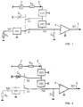
- the reference adjustment is in Figs. 1 and 2 shown.
- the reference resistor R0 is connected to the input M0.
- a first step (switches S1 and S2 in position 1), R0 is connected to reference point M2 via VP1 and switch S1 and Z abg is separated using switch S2. (Fig. 1).
- This corresponds to the normal operating state, except that the desired resistance R0 is at the input M0 instead of the actual probe head impedance Z x and the HF generator 2 is switched on.
- the RF tuning signal 3 whose frequency is periodically varied linearly between two values, generates a signal at the reference point M2, which reaches the computer via the preamplifier 4, receiver, quadrature detector and AD converter (not shown). An entire period of this signal is stored vectorially and is referred to as the first reference signal.
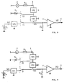
- a second step switching S1 and S2 in position 2
- R0 is separated from point M2 using switch S1 and the reference impedance Z captive is switched on via switch S2 (FIG. 2).
- the next period of the RF tuning signal 3 generates a new signal at point M2, which is measured analogously to the first step and stored vectorially.
- This signal hereinafter referred to as the second reference signal, is vectorially subtracted from the reference signal 1 and the absolute value is formed therefrom.
- This gives the difference signal A which is displayed on the screen as a y signal.
- the x signal is defined by the frequency variation.
- the probe head impedance Z x must be at input M0.
- the voting process is shown in FIGS. 3 and 4. Two steps are also required.
- the second reference signal is measured during a period of the linear frequency variation and stored vectorially (FIG. 3).
- a second step switching S1 and S2 in position 1
- the signal dependent on the probe head impedance Z x is measured at point M2 during the next period of the linear frequency variation (FIG. 4), stored vectorially, vectorially subtracted from the second reference signal and of that Absolute value formed.
- This signal is referred to as difference signal B. It is displayed on the screen as a y signal.
- the x signal is in turn defined by the frequency variation.
- step 1 The two steps are repeated periodically, so that during the tuning of the probe head impedance Z x a variable image appears on the screen, which has the shape of a vertically mirrored resonance curve.
- step 1 the repetition of step 1 must not be omitted. This is because slow fluctuations in the signal level of the HF generator 2 must be expected during the duration of the tuning process, and these change the second reference signal.
- the tuning process is complete when the minimum of the curve is approximately zero and at the desired frequency point.
- connection to the probe head or to the probe head impedance Z x must also be switched on and off periodically.
- a series switch for example in the form of the ideal series switch S1 shown in FIG. 7 in path 9 of the NMR signal, is therefore unavoidable.
- a low-loss series switch which manages in the closed state with a blocked diode D3. If U S is negative, then the pin diode D3 blocks, and the point M1 is connected via the two ⁇ / 4 lines 6, 7 to point M2 directly and with little loss. This corresponds to the closed state of the series switch. This state prevails in the normal operating state of the receiving system, and small signal losses should be realized here.
- a blocking diode is therefore better than a conductive one because the former causes somewhat smaller losses.
- This type of series switch has the property that the switching diode blocks in the closed state and conducts in the open state. This is just the opposite of the behavior compared to the known arrangement (Fig. 8) where the switching diode is in series with path 9 of the NMR signal.
- the switch S0 already has all the RF components required for the series switch S1, but also additionally the diode chain Dk and the diode D4, which do not interfere with the functioning of S1. It is thus possible to implement the series switch S1 without the introduction of additional components, and this at least saves a diode (D 1), a choke (Z Dr ) and a capacitance (C 1) compared to the prior art shown in FIG. 6.
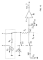
- FIGS. 5 and 6 show a first circuit arrangement according to the invention, in which the reference impedance Z0 is separated from the path 9 of the NMR signal by the high-impedance coupling impedance Z k .
- the areas outlined with dashed lines refer to the areas shown in FIGS. 5 and 6 used function blocks.
- VP1 does not appear in FIG. 10.
- VP1 can mean, for example, an impedance transformer with which an additional impedance transformation from point M0 to point M2 is achieved in the normal operating state. But since this transformation is only used in very special cases 10, it is omitted.
- the circuit in Fig. 10 uses the variant with only one tunable reference impedance Z0. This can be achieved by a variable resistor R ZO of approx. 100 ⁇ in parallel with a trimmer C ZO of approx. 15 pF. C ZO mainly takes into account the parasitic reactances still present within the circuit.
- the attenuator 8 in the four-pole VP3 separates the HF generator 2 from the reference impedance Z0. This ensures that the HF generator 2 and the associated connecting line are always matched impedance, i.e. always see the correct load resistance, regardless of the tuning of Z0.
- Fig. 11 shows a second circuit arrangement according to the invention, in which the reference impedance Z0 is present directly on the path 9 of the NMR signal.
- the four-pin VP2 is degenerated into a direct connection.
- VP3 contains the coupling impedance Z k .
- the attenuator 8 is no longer required, since Z0 is separated from the HF generator 2 by Z k and therefore cannot act on the HF generator 2.
- the switch S2 was supplemented by a second pin diode D5, which is open when switch S2 is open (ie, D2 blocked) and thereby short-circuits Z0. This prevents the active component of Z0 from being transformed into the path 9 of the NMR signal via the parasitic capacitance of the blocking diode D2 and there leading to a deterioration in the S / N ratio.
- the circuit arrangement shown in Fig. 11 is somewhat disadvantageous compared to the circuit shown in Fig. 10 because it contains one more diode (D2) on path 9 of the NMR signal. However, this locks in the normal operating state and thus introduces slightly less losses than if it were to conduct. In addition, the diode D5 prevents an additional deterioration in the S / N ratio due to the influence of Z0.
- the lengths of the two ⁇ / 4 lines 6, 7 of the changeover switch S0 do not have to be exactly a length of ⁇ / 4.
- the second ⁇ / 4 line 7 can have deviations of up to ⁇ 40% and still suppress the remaining portion of the RF transmission pulse 12 sufficiently with the aid of the diode D4. Maintaining the length of the first ⁇ / 4 line 6 is, however, more critical.
- an inaccurate length leads to a mismatch and power reflection of the RF transmission pulse 12 at point M0, which must not be too large.
- tolerances of ⁇ 5% are also permitted here.
- the lengths of the ⁇ / 4 lines 6, 7 of the HF series switch in FIG. 9 also need not be exactly ⁇ / 4. Deviations of up to ⁇ 40% are tolerable here too, because they primarily only cause (capacitive and inductive) reactive loads at the input and output of the switch.
Landscapes
- Physics & Mathematics (AREA)
- Condensed Matter Physics & Semiconductors (AREA)
- General Physics & Mathematics (AREA)
- Magnetic Resonance Imaging Apparatus (AREA)
Applications Claiming Priority (2)
| Application Number | Priority Date | Filing Date | Title |
|---|---|---|---|
| DE4428579 | 1994-08-12 | ||
| DE4428579A DE4428579C1 (de) | 1994-08-12 | 1994-08-12 | Verfahren und automatische Hilfsvorrichtung zur Abstimmung einer NMR-Empfangsspule |
Publications (3)
| Publication Number | Publication Date |
|---|---|
| EP0696743A2 true EP0696743A2 (fr) | 1996-02-14 |
| EP0696743A3 EP0696743A3 (fr) | 1996-06-26 |
| EP0696743B1 EP0696743B1 (fr) | 1999-12-15 |
Family
ID=6525534
Family Applications (1)
| Application Number | Title | Priority Date | Filing Date |
|---|---|---|---|
| EP95108822A Expired - Lifetime EP0696743B1 (fr) | 1994-08-12 | 1995-06-08 | Méthode et dispositif auxiliaire pour l'accord d'une bobine de détection RMN |
Country Status (4)
| Country | Link |
|---|---|
| US (1) | US5552710A (fr) |
| EP (1) | EP0696743B1 (fr) |
| JP (1) | JP3597262B2 (fr) |
| DE (2) | DE4428579C1 (fr) |
Families Citing this family (5)
| Publication number | Priority date | Publication date | Assignee | Title |
|---|---|---|---|---|
| FR2819891B1 (fr) * | 2001-01-24 | 2003-08-15 | Bruker Sa | Circuit d'excitation et de recuperation du signal emis par une sonde dans un appareil de spectrometrie rmn |
| US6774634B2 (en) | 2002-01-29 | 2004-08-10 | Varian, Inc. | Automated NMR analysis using solvents and sample tube materials to control frequency shifts |
| US20030173966A1 (en) * | 2002-03-14 | 2003-09-18 | Thr Board Of Trustees Of The Leland Stanford Junior University | Varactor tuned flexible interventional receiver coils |
| US6833704B1 (en) | 2003-07-21 | 2004-12-21 | Varian, Inc. | Multinuclear wands |
| US7595641B1 (en) * | 2008-03-07 | 2009-09-29 | Varian, Inc. | Electronic NMR reference signal systems and methods |
Citations (1)
| Publication number | Priority date | Publication date | Assignee | Title |
|---|---|---|---|---|
| DE3838252A1 (de) | 1988-11-11 | 1990-05-17 | Spectrospin Ag | Verfahren zum abstimmen des probenkopfes eines nmr-spektrometers und zur durchfuehrung des verfahrens ausgebildetes nmr-spektrometer |
Family Cites Families (4)
| Publication number | Priority date | Publication date | Assignee | Title |
|---|---|---|---|---|
| DE3374813D1 (en) * | 1982-12-28 | 1988-01-14 | Toshiba Kk | Nuclear magnetic resonance diagnostic apparatus |
| US4593246A (en) * | 1984-09-12 | 1986-06-03 | Varian Associates, Inc. | NMR tuning procedure |
| JPH01201244A (ja) * | 1988-02-08 | 1989-08-14 | Toshiba Corp | Mri装置のインピーダンス自動調整装置 |
| JP2965178B2 (ja) * | 1991-10-15 | 1999-10-18 | 日本電子株式会社 | 核磁気共鳴装置における送受信回路 |
-
1994
- 1994-08-12 DE DE4428579A patent/DE4428579C1/de not_active Expired - Fee Related
-
1995
- 1995-06-08 DE DE59507419T patent/DE59507419D1/de not_active Expired - Lifetime
- 1995-06-08 EP EP95108822A patent/EP0696743B1/fr not_active Expired - Lifetime
- 1995-07-10 US US08/499,856 patent/US5552710A/en not_active Expired - Lifetime
- 1995-08-14 JP JP20722795A patent/JP3597262B2/ja not_active Expired - Lifetime
Patent Citations (1)
| Publication number | Priority date | Publication date | Assignee | Title |
|---|---|---|---|---|
| DE3838252A1 (de) | 1988-11-11 | 1990-05-17 | Spectrospin Ag | Verfahren zum abstimmen des probenkopfes eines nmr-spektrometers und zur durchfuehrung des verfahrens ausgebildetes nmr-spektrometer |
Also Published As
| Publication number | Publication date |
|---|---|
| DE59507419D1 (de) | 2000-01-20 |
| US5552710A (en) | 1996-09-03 |
| EP0696743B1 (fr) | 1999-12-15 |
| EP0696743A3 (fr) | 1996-06-26 |
| JP3597262B2 (ja) | 2004-12-02 |
| JPH0862314A (ja) | 1996-03-08 |
| DE4428579C1 (de) | 1996-02-01 |
Similar Documents
| Publication | Publication Date | Title |
|---|---|---|
| DE69427563T2 (de) | Abstimmbarer Filter | |
| DE3608473C2 (de) | HF-Oberflächensonde für Magnetresonanzsysteme mit zwei Betriebsfrequenzen | |
| DE2104779C3 (de) | Bandfilter-Schaltung | |
| DE3832293C2 (de) | Anpassungsschaltung | |
| DE10325634B4 (de) | Rauscharmer Vorverstärker, insbesondere für die Kernspinresonanz(=NMR) | |
| DE3923661A1 (de) | Schaltungsanordnung fuer die anpassung der impedanz einer plasmastrecke an einen hochfrequenzgenerator | |
| DE2905821C2 (de) | Anordnung zur gleichstromisolierten Kopplung von HF-Signalen auf einen Fernsehempfänger | |
| DE3629356A1 (de) | Abstimmschaltung fuer ein kernmagnetresonanz-sende- und empfangssystem | |
| EP0818888B1 (fr) | Filtre passe-bande commutable pour tuner multi-gammes | |
| DE2125341B2 (de) | Resonator mit veränderlicher Resonanzfrequenz | |
| EP0696743B1 (fr) | Méthode et dispositif auxiliaire pour l'accord d'une bobine de détection RMN | |
| DE4291983C2 (de) | Abstimmbare Höchstfrequenz-Bandsperrfiltereinrichtung | |
| EP1887373A1 (fr) | Installation de détection par résonance magnétique (RM) atténuée passivement et procédé destiné à l'atténuation de circuit oscillant HF d'une telle installation de détection RM | |
| DE69204152T2 (de) | Elektronische Vorrichtung zur Multiplexierung verschiedener mit Wechselstrom gespeisster Läste. | |
| DE69215589T2 (de) | Mikrowellen-Vorspannungseinstellungsschaltung | |
| DE60021036T2 (de) | Sende-Empfangsumschalter | |
| DE102019101888B4 (de) | Konfigurierbares mikroakustisches HF-Filter | |
| DE102005037877A1 (de) | Diodenmischer | |
| EP3081953A2 (fr) | Systeme de bobine de reception et d'emission nmr | |
| DE69716146T2 (de) | Hochfrequenz-Leistungsmesseinrichtung | |
| DE69314597T2 (de) | Variabler Hochfrequenzleistungsverteiler | |
| DE4024800A1 (de) | Reflexions-nebenschlussdioden-hf-modulator | |
| DE4122797A1 (de) | Spulenanordnung fuer messungen mittels magnetischer resonanz | |
| DE3234736C1 (de) | Schaltung zur Gleichstromspeisung von Transistoren | |
| DE102023204070A1 (de) | Spule, Spulenanordnung und Verfahren |
Legal Events
| Date | Code | Title | Description |
|---|---|---|---|
| PUAI | Public reference made under article 153(3) epc to a published international application that has entered the european phase |
Free format text: ORIGINAL CODE: 0009012 |
|
| AK | Designated contracting states |
Kind code of ref document: A2 Designated state(s): CH DE FR GB LI |
|
| PUAL | Search report despatched |
Free format text: ORIGINAL CODE: 0009013 |
|
| AK | Designated contracting states |
Kind code of ref document: A3 Designated state(s): CH DE FR GB LI |
|
| 17P | Request for examination filed |
Effective date: 19960531 |
|
| 17Q | First examination report despatched |
Effective date: 19971125 |
|
| RAP1 | Party data changed (applicant data changed or rights of an application transferred) |
Owner name: BRUKER AG |
|
| GRAG | Despatch of communication of intention to grant |
Free format text: ORIGINAL CODE: EPIDOS AGRA |
|
| GRAG | Despatch of communication of intention to grant |
Free format text: ORIGINAL CODE: EPIDOS AGRA |
|
| GRAH | Despatch of communication of intention to grant a patent |
Free format text: ORIGINAL CODE: EPIDOS IGRA |
|
| GRAH | Despatch of communication of intention to grant a patent |
Free format text: ORIGINAL CODE: EPIDOS IGRA |
|
| GRAA | (expected) grant |
Free format text: ORIGINAL CODE: 0009210 |
|
| AK | Designated contracting states |
Kind code of ref document: B1 Designated state(s): CH DE FR GB LI |
|
| REG | Reference to a national code |
Ref country code: CH Ref legal event code: EP |
|
| REG | Reference to a national code |
Ref country code: CH Ref legal event code: NV Representative=s name: RIEDERER HASLER & PARTNER PATENTANWAELTE AG |
|
| REF | Corresponds to: |
Ref document number: 59507419 Country of ref document: DE Date of ref document: 20000120 |
|
| ET | Fr: translation filed | ||
| GBT | Gb: translation of ep patent filed (gb section 77(6)(a)/1977) |
Effective date: 20000324 |
|
| PLBE | No opposition filed within time limit |
Free format text: ORIGINAL CODE: 0009261 |
|
| STAA | Information on the status of an ep patent application or granted ep patent |
Free format text: STATUS: NO OPPOSITION FILED WITHIN TIME LIMIT |
|
| 26N | No opposition filed | ||
| REG | Reference to a national code |
Ref country code: GB Ref legal event code: IF02 |
|
| REG | Reference to a national code |
Ref country code: CH Ref legal event code: PFA Free format text: BRUKER AG TRANSFER- BRUKER BIOSPIN AG |
|
| REG | Reference to a national code |
Ref country code: FR Ref legal event code: CD |
|
| REG | Reference to a national code |
Ref country code: CH Ref legal event code: PCAR Free format text: RIEDERER HASLER & PARTNER PATENTANWAELTE AG;ELESTASTRASSE 8;7310 BAD RAGAZ (CH) |
|
| PGFP | Annual fee paid to national office [announced via postgrant information from national office to epo] |
Ref country code: CH Payment date: 20110623 Year of fee payment: 17 Ref country code: FR Payment date: 20110630 Year of fee payment: 17 |
|
| PGFP | Annual fee paid to national office [announced via postgrant information from national office to epo] |
Ref country code: GB Payment date: 20110621 Year of fee payment: 17 |
|
| REG | Reference to a national code |
Ref country code: CH Ref legal event code: PL |
|
| REG | Reference to a national code |
Ref country code: CH Ref legal event code: PL |
|
| GBPC | Gb: european patent ceased through non-payment of renewal fee |
Effective date: 20120608 |
|
| REG | Reference to a national code |
Ref country code: FR Ref legal event code: ST Effective date: 20130228 |
|
| PG25 | Lapsed in a contracting state [announced via postgrant information from national office to epo] |
Ref country code: CH Free format text: LAPSE BECAUSE OF NON-PAYMENT OF DUE FEES Effective date: 20120630 Ref country code: GB Free format text: LAPSE BECAUSE OF NON-PAYMENT OF DUE FEES Effective date: 20120608 Ref country code: FR Free format text: LAPSE BECAUSE OF NON-PAYMENT OF DUE FEES Effective date: 20120702 Ref country code: LI Free format text: LAPSE BECAUSE OF NON-PAYMENT OF DUE FEES Effective date: 20120630 |
|
| PGFP | Annual fee paid to national office [announced via postgrant information from national office to epo] |
Ref country code: DE Payment date: 20140626 Year of fee payment: 20 |
|
| REG | Reference to a national code |
Ref country code: DE Ref legal event code: R071 Ref document number: 59507419 Country of ref document: DE |