EP0697257A2 - Pietoelectrischer-Komposit Wandleranordnung mit verbesserter akustischer und elektrischer Impedanz - Google Patents
Pietoelectrischer-Komposit Wandleranordnung mit verbesserter akustischer und elektrischer Impedanz Download PDFInfo
- Publication number
- EP0697257A2 EP0697257A2 EP95107745A EP95107745A EP0697257A2 EP 0697257 A2 EP0697257 A2 EP 0697257A2 EP 95107745 A EP95107745 A EP 95107745A EP 95107745 A EP95107745 A EP 95107745A EP 0697257 A2 EP0697257 A2 EP 0697257A2
- Authority
- EP
- European Patent Office
- Prior art keywords
- electrodes
- opposing
- wafers
- transducer
- composite
- Prior art date
- Legal status (The legal status is an assumption and is not a legal conclusion. Google has not performed a legal analysis and makes no representation as to the accuracy of the status listed.)
- Withdrawn
Links
Images



Classifications
-
- B—PERFORMING OPERATIONS; TRANSPORTING
- B06—GENERATING OR TRANSMITTING MECHANICAL VIBRATIONS IN GENERAL
- B06B—METHODS OR APPARATUS FOR GENERATING OR TRANSMITTING MECHANICAL VIBRATIONS OF INFRASONIC, SONIC, OR ULTRASONIC FREQUENCY, e.g. FOR PERFORMING MECHANICAL WORK IN GENERAL
- B06B1/00—Methods or apparatus for generating mechanical vibrations of infrasonic, sonic, or ultrasonic frequency
- B06B1/02—Methods or apparatus for generating mechanical vibrations of infrasonic, sonic, or ultrasonic frequency making use of electrical energy
- B06B1/06—Methods or apparatus for generating mechanical vibrations of infrasonic, sonic, or ultrasonic frequency making use of electrical energy operating with piezoelectric effect or with electrostriction
- B06B1/0607—Methods or apparatus for generating mechanical vibrations of infrasonic, sonic, or ultrasonic frequency making use of electrical energy operating with piezoelectric effect or with electrostriction using multiple elements
- B06B1/0622—Methods or apparatus for generating mechanical vibrations of infrasonic, sonic, or ultrasonic frequency making use of electrical energy operating with piezoelectric effect or with electrostriction using multiple elements on one surface
-
- H—ELECTRICITY
- H10—SEMICONDUCTOR DEVICES; ELECTRIC SOLID-STATE DEVICES NOT OTHERWISE PROVIDED FOR
- H10N—ELECTRIC SOLID-STATE DEVICES NOT OTHERWISE PROVIDED FOR
- H10N30/00—Piezoelectric or electrostrictive devices
- H10N30/01—Manufacture or treatment
- H10N30/07—Forming of piezoelectric or electrostrictive parts or bodies on an electrical element or another base
- H10N30/074—Forming of piezoelectric or electrostrictive parts or bodies on an electrical element or another base by depositing piezoelectric or electrostrictive layers, e.g. aerosol or screen printing
- H10N30/077—Forming of piezoelectric or electrostrictive parts or bodies on an electrical element or another base by depositing piezoelectric or electrostrictive layers, e.g. aerosol or screen printing by liquid phase deposition
-
- H—ELECTRICITY
- H10—SEMICONDUCTOR DEVICES; ELECTRIC SOLID-STATE DEVICES NOT OTHERWISE PROVIDED FOR
- H10N—ELECTRIC SOLID-STATE DEVICES NOT OTHERWISE PROVIDED FOR
- H10N30/00—Piezoelectric or electrostrictive devices
- H10N30/80—Constructional details
- H10N30/85—Piezoelectric or electrostrictive active materials
- H10N30/852—Composite materials, e.g. having 1-3 or 2-2 type connectivity
-
- H—ELECTRICITY
- H04—ELECTRIC COMMUNICATION TECHNIQUE
- H04R—LOUDSPEAKERS, MICROPHONES, GRAMOPHONE PICK-UPS OR LIKE ACOUSTIC ELECTROMECHANICAL TRANSDUCERS; ELECTRIC HEARING AIDS; PUBLIC ADDRESS SYSTEMS
- H04R17/00—Piezoelectric transducers; Electrostrictive transducers
- H04R17/04—Gramophone pick-ups using a stylus; Recorders using a stylus
- H04R17/08—Gramophone pick-ups using a stylus; Recorders using a stylus signals being recorded or played back by vibration of a stylus in two orthogonal directions simultaneously
-
- Y—GENERAL TAGGING OF NEW TECHNOLOGICAL DEVELOPMENTS; GENERAL TAGGING OF CROSS-SECTIONAL TECHNOLOGIES SPANNING OVER SEVERAL SECTIONS OF THE IPC; TECHNICAL SUBJECTS COVERED BY FORMER USPC CROSS-REFERENCE ART COLLECTIONS [XRACs] AND DIGESTS
- Y10—TECHNICAL SUBJECTS COVERED BY FORMER USPC
- Y10T—TECHNICAL SUBJECTS COVERED BY FORMER US CLASSIFICATION
- Y10T29/00—Metal working
- Y10T29/42—Piezoelectric device making
-
- Y—GENERAL TAGGING OF NEW TECHNOLOGICAL DEVELOPMENTS; GENERAL TAGGING OF CROSS-SECTIONAL TECHNOLOGIES SPANNING OVER SEVERAL SECTIONS OF THE IPC; TECHNICAL SUBJECTS COVERED BY FORMER USPC CROSS-REFERENCE ART COLLECTIONS [XRACs] AND DIGESTS
- Y10—TECHNICAL SUBJECTS COVERED BY FORMER USPC
- Y10T—TECHNICAL SUBJECTS COVERED BY FORMER US CLASSIFICATION
- Y10T29/00—Metal working
- Y10T29/49—Method of mechanical manufacture
- Y10T29/49002—Electrical device making
- Y10T29/49117—Conductor or circuit manufacturing
- Y10T29/49124—On flat or curved insulated base, e.g., printed circuit, etc.
- Y10T29/49155—Manufacturing circuit on or in base
Definitions
- This invention relates to transducer elements used in transducer arrays, such as linear arrays, phased arrays, and two-dimensional arrays, and more particularly to a composite piezoelectric transducer element having a good match of both acoustical impedance with the body and electrical impedance with the imaging system.
- Acoustic transducers for medical ultrasonic imaging are made of piezoelectric materials.
- a variety of composite materials are made by combining a piezoelectric ceramic with a passive polymer phase. These composite materials extend the range of material properties offered by conventional piezoelectric ceramics and polymers.
- the 1-3 PZT rod-polymer composite structure 10 shown in Fig. 1 consists of a polymer matrix 11 which holds together thin parallel rods 12 of piezoelectric ceramic oriented perpendicular to opposing faces 13, 14 of the plate. Metal electrodes are applied to the faces 13, 14.
- Important parameters for a successful piezo material in this application include: sensitivity; acoustical and electrical impedance matching; low electrical and mechanical losses; shapability; thermal stability and structural strength.
- the piezoelectric must efficiently convert between electrical and mechanical energy, so that the electromechanical coupling is high.
- the piezoelectric must be acoustically matched to the tissue so that the acoustic waves in the transducer and the tissue couple well during both transmission and reception.
- Each of the array elements electric impedance must be compatible with the driving and receiving electronics, which is usually 50 ohms.
- the electrical impedance is inversely proportional to the dielectric constant of the piezoelectric material.
- the dielectric constant must be relatively large.
- a good piezoelectric material for medical ultrasonic imaging should have: high electro-mechanical coupling (k t approaching 1); acoustic impedance close to that of the tissue (Z approaching 1.5 Mrayls); reasonably large dielectric constant ( ⁇ s ⁇ 100); and low electrical (tan ⁇ ⁇ 0.10) and mechanical (Q m ⁇ 10) losses. See Smith at p. 249.
- the performance of a composite piezoceramic varies with the volume fraction of piezoceramic for a given ceramic and polymer. Generally, a trade-off is made between lowering the acoustic impedance and obtaining a high coupling as the volume fraction decreases. Nevertheless, there is a broad range of proportions over which the composite's coupling coefficient is higher and its acoustic impedance lower than those of a pure piezoceramic component. Smith at p. 253.
- Transducer arrays have been made from composites, as shown for example in Fig. 2.
- a composite linear array 20 has rectangular ceramic rods 21 embedded in a polymer matrix 22, with metal electrodes 23, 24 on opposed major surfaces of the composite 27, a matching layer 25 on one major surface for placement adjacent the body, and array elements 26 defined by an electrode pattern on the second major surface.
- arrays can be made by cutting the composite to isolate array elements.
- Composites can be made quite flexible, enabling formation into curved shapes for beam focusing and steering.
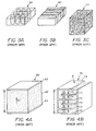
- Fig. 3 illustrates schematically three of the various types of composite piezoelectric materials.
- the composite types are referred to by the connectivity pattern of the individual phases.
- a 1-3 connectivity refers to a composite with a piezoelectric phase continuous or self-connected in one dimension and a polymer phase self-connected in three dimensions.
- Fig. 3A shows the 1-3 PZT rods in a polymer structure 30, as previously discussed in regard to Figs. 1-2.
- Fig. 3B illustrates a layered 2-2 structure 40, comprising alternating layers of piezoceramic and polymer, wherein electrodes are placed on the opposing top and bottom surfaces.
- Fig. 3C illustrates a 3-3 composite structure 50, comprising a blend of piezoceramic and polymer.
- Each of these structures has advantages in different applications. In general, a device structure having a low Q is desired, which is best achieved by efficiently coupling the transducer acoustically to the medium and electrically to the excitation
- Goldberg et al. uses multi-layer ceramics to increase both the transmit and receive sensitivity of a 2-D array element.
- the goal is to increase the acoustic output power into the body tissue for a given source voltage, which is accomplished by matching the electrical impedances of the source and the transducer for maximum power transfer.
- the receive mode the goal is to increase the received voltage that is amplified and processed by the ultrasound imaging system; the received voltage is increased by having a matched transducer impedance relative to the coaxial cable and imaging circuitry.
- the capacitance C N of an N layer transducer with an electrode area A, layer thickness t/N, and dielectric constant ⁇ is:
- C single is the capacitance of a single layer transducer (such as element 60 in Fig. 4A having a single ceramic layer 62 between electrodes 63, 64).
- the open-circuit receive sensitivity is directly proportional to the layer thickness t/N, and as a result increasing the number of layers will decrease the open-circuit sensitivity.
- the authors state that the multilayer ceramic structure's ability to drive an electrical load compensates for the decreased open-circuit sensitivity.
- Two-dimensional arrays consist of tiny transducer elements distributed in a square lattice in two dimensions.
- One of the major problems in 2-D arrays is that element sizes are very tiny which results in extremely large electrical impedance.
- the electrical impedance ranges from a couple of hundred ohms to larger than a kilo ohm depending on the frequency and aperture of the elements.
- each one of these elements are subdivided into 64 or larger number of elements in the elevation direction.
- the impedance of each of the 2-D array elements is at least 64 times larger and makes it difficult to couple the electrical energy from the typically 50 ohm imaging system to the transducer.
- the present invention solves this electrical impedance problem along with optimizing the acoustic impedance match to the human body.
- the present invention is directed to a new composite structure providing thin wafers of piezoceramic which are electroded on opposing major first and second surfaces and polarized along the thickness between the electrodes.
- the wafers are spaced apart by a layer of passive polymer.
- An element includes at least two electroded ceramic wafers and an intermediate passive polymer layer.
- the piezoelectric wafers are driven electrically along the wafer thickness to generate acoustic vibration in the perpendicular direction (see Fig. 7). This mode of vibration is referred to as transverse '31' mode.
- the elements can be provided in a 2-2 or 3-1 composite structure.
- the number of wafers in a given element can be selected to provide a desired impedance match.
- a linear or phased array there may be hundreds of wafers provided in a strip.
- a 2-D array a plurality of such elements can be provided in a square lattice in two dimensions.
- the ceramic wafers interspersed with polymer layers results in a low acoustic impedance composite structure.
- both electrical impedance and acoustic impedance are optimized for tiny array elements.
- Another aspect of the present invention are various methods of making the composite structure.
- wafers of piezoelectric ceramic are electroded along their major surfaces and polarized along the thickness.
- the wafers are stacked with spacers along one edge to build a stack of tens or hundreds of wafers, depending on the desired application.
- the stack is then cast in an epoxy polymer matrix.
- the area containing the spacers is trimmed away to provide the composite structure.
- the original surface electrodes extend to the edges of the element, channels are cut into the composite at regular intervals along opposite edges and the channels are then filled with polymer. End electrodes are provided on the top and bottom surfaces of the element respectively, each connected to a different one of the two sets of surface electrodes.
- the surface electrodes may be originally applied for example, by masking, such that they do not extend to the opposing edge, in which case channels are not required.
- a further alternative method of preparation is to start with a piezoceramic block and to dice grooves with a diamond saw blade to form a series of spaced parallel piezoceramic wafers. The wafers are then electroded and the grooves filled with epoxy. A bottom piezoceramic layer is cut off to produce a composite structure. Again channels are cut on opposing surfaces to provide two sets of opposing surface electrodes, the channels filled with polymer, and end electrodes applied.
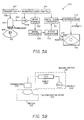
- FIG. 5A A block diagram of a phased-array, pulse-echo ultrasound imaging system 100 is shown in Fig. 5A.
- the system provides a pulsed electrical stimulus to an array of transducers 101, which causes the transducers to transmit an ultrasonic acoustical wave 103.
- the wave is transmitted into a medium, such as a human body, and eventually, at least partially reflected by an object (e.g., heart 115) in the medium.
- the reflected wave (the "echo”) is received by the transducers 101, which produce an electrical signal 104 that is indicative of the echo.
- Various properties of the electrical signal caused by the echo are then analyzed by a signal processing section of the imaging system to determine information about the object, such as its size, location, and velocity.
- the imaging system may use beam steering, phased array, or other techniques known in the art to stimulate the transducers and to analyze the electrical signal resulting from the echo, see e.g., U.S. Patent No. 5,060,651 entitled "Ultrasonic Diagnostic Apparatus.”
- Fig. 5A shows a microprocessor 108 for controlling each of a transmitter 107, preamplifier 109, beam former 106, and digital scan converter 111.
- the echo signal 104 from transducer array 101 is sent to preamplifier 109 which amplifies the same, and then in series to beam former 106, signal processor 105, A-D converter 110, and digital scan converter 111.
- the z component is sent to post-processor 112, and the resulting z intensity is displayed on CRT screen 114.
- the x-y component is sent via x-y raster 113 and displayed on CRT screen 114. Any number of different transmitting and imaging processing systems may be used.
- Fig. 5B illustrates in simplified form how a transducer 120 is electrically coupled to an imaging system 121 at one side, and acoustically coupled to the medium (a patient 122) at another side.
- the imaging system may for example include a source 123 with an approximate electrical impedance of 50 ohms in series with a cable 124 having a 50 ohm impedance.
- the condition of maximum power transfer to the load (patient 122) occurs when the source and cable impedances and transducer impedance are substantially identical.
- the incident acoustic pressure can be modeled as a voltage source, while the transducer impedance becomes the source impedance.
- the electrical load consists of the shunt capacitance of the cable and the preamplifier input impedance.
- the transducer can drive the cable load effectively when the transducer capacitance is much greater than the cable capacitance.
- the composite element of the present invention satisfies these requirements.
- C ⁇ o KA/d
- K the relative dielectric constant
- ⁇ o the permittivity of free space (8.85 x 10 ⁇ 12 farads/meter)
- A is the area facing the parallel plates
- d is the distance between the plates.
- Transducer element 200 has a square cross section, 250 microns ( ⁇ ) on each of two sides 201, 202, and a height d between opposing electrodes 203, 204 of approximately 500 microns.
- a first embodiment of the present invention utilizes a 2-2 composite structure wherein a plurality of wafer elements 210 (see Fig. 7) are sandwiched between polymer layers to form a composite element 230 (see Fig. 8).
- Fig. 7 shows one relatively thin PZT wafer 211, having a thickness t (in the x direction), and major opposing surfaces 212, 213 (in the y-z plane) each with a relatively large area A.
- the major opposing surfaces are electroded 214, 215 over a majority of their large surface area, and the wafer is poled across the thickness (in the x direction as shown by arrow 216).
- the resulting acoustic output signal 217 is in the z direction.
- the capacitance of this wafer element is relatively large because of the large electrode area and relatively small thickness t. Furthermore, when a plurality of these wafers are electrically connected in parallel, their capacitance is summed, producing a large capacitance and correspondingly small electrical impedance for improved matching with the imaging system.
- the relative dimensions and number of the elements can vary; preferably the thickness, area and number of elements are selected to provide an impedance of each element of about 50 ohms.
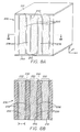
- Figs. 8A-B illustrate front perspective and cross-sectional views respectively of the composite 2-2 transducer 230 of this invention.
- Flat wafers or strips 235 of piezoelectric ceramic, such as PZT are sandwiched between a first electrode layer 240 on one side and a second electrode layer 242 on the other side.
- the electrodes extend along the major surfaces of the wafers, in the y-z plane.
- Each set of electrodes 240, 242 is connected to a different one of end electrodes 241, 243 at opposing top and bottom surfaces of the composite.
- upwardly-depending electrodes 240 are connected to top end electrode 241, and terminate short of the bottom electrode 243.
- downwardly-extending electrodes 242 connect to bottom electrode 243, and end short of the top electrode 241.
- a layer of passive polymer 238, for improved acoustical matching with the body, is provided between each adjacent set of electroded wafers 240/235/242.
- the wafers 235 are polarized across their thickness in the x direction and are stimulated with an electrical pulse along the same direction. As such, the wafers 235 are driven using the k31 coupling of the PZT material, and resonance occurs along the z direction.
- Each combination 250 of an electrode 240, wafer 235, and electrode 242 may be modeled as a parallel plate capacitor. Moreover, the arrangement of Figs. 8A-8B define a plurality of such capacitors connected in parallel. Thus, the overall capacitance of the composite 230 is the sum of the individual capacitance for each combination 250. Because each combination 250 provides a relatively large electrode surface area and a relatively small distance t between electrodes, each combination 250 has a relatively high capacitance.
- the prior art transducer of Fig. 6 has a capacitance of approximately 3.3pf.
- the composite 230 of this invention having a PZT wafer 235 that is 50 microns wide, sandwiched between electrodes 240 and 242 will exhibit approximately 66pf of capacitance per combination 250.
- 25 micron thick polymer layers 238 separate the combinations 250 three such combinations connected in parallel will fit in the same volume as the prior art transducer. Consequently, the transducer 230 will exhibit a total capacitance of approximately 198pf.
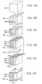
- Figs. 9A-9G illustrate one method of forming a composite element 230.
- Wafers 235 of PZT material are electroplated (or electrodes applied by other means) on their opposing major surfaces 236 and 237 (see Fig. 9A). Each wafer may be 50 microns thick, for example.
- the wafers 235 are polarized (i.e., poled) along the thickness t so that the PZT exhibits piezoelectric properties.
- the electroded wafers are then stacked with spacers 261 at lower edge 260, thus separating the major surfaces 236 and 237 of adjacent wafers (see Fig. 9B).
- Each spacer 261 may be 25 microns thick, for example.
- the number of wafers that are stacked depends upon the application, but the stack 262 may include tens or hundreds of such wafers, if necessary.
- the entire stack 262 is then cast in an epoxy matrix, forming polymer layers 238 which fill the spaces between the ceramic wafers 235 (see Fig. 9C).
- a bottom portion 264 of the stack which includes the spacers is trimmed away by a diamond saw blade, as shown in Fig. 9D.
- the polymer filled stack 263 is then cut into transverse sections of transducer elements 230 (Fig. 9E) of the appropriate size.
- the transducer elements 230 are ground, with a dicing saw for example, to form channels 265, 266 in opposing ends of electrodes 236, 237, respectively.
- the channels are necessary so that electrodes 236, 237 will not be in electrical connection, when end surfaces 241, 243 are electroded, as described below.
- the channels may extend for 25 microns, for example, as shown in Fig. 9F.
- the channels 265, 266 are filled with polymer 238, and the opposing transverse surfaces 241, 243 are electroded (see Fig. 9G).
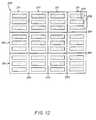
- the transducers 230 are then arranged into 2-D arrays with techniques known in the art (see Fig. 12).
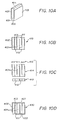
- Figs. 10A-10D illustrate another method of forming a composite element 430, in which the original electrodes extend over less than the entire surface of the wafer.
- a piezoceramic wafer 401 has opposing surface electrodes 402 and 403 extending over a substantial majority of the opposing surfaces, but terminating short of opposing top and bottom end surfaces 405, 406.
- Fig. 10B a plurality of such elements are placed in spaced relation by a series of spacers 412 along one edge, and the areas between the wafers are filled with polymer to form polymer layers 411 in composite block 410.
- a bottom portion 413 including the spacers is cut off, and a top portion 412 is lapped off as shown in Fig. 10C, exposing the opposing sets of electrodes 402, 403 on the central portion 414.
- upper and lower electrodes 421 and 422 are applied to the top and bottom of the composite to form the finished transducer element 430.
- FIGs. 11A-11F A further alternative method of producing a composite 330 is shown in Figs. 11A-11F.
- a PZT block 300 is diced to form elongated parallel channels 336 (Fig. 11B), by for example a diamond saw.
- the channels 336 separate extending rectangular projections or wafers 337, which are joined along one common edge 339.
- the upper surface of the element including side surfaces of each projection 337 are covered with electrodes 332, 334, by for example sputtering or vacuum deposition (Fig. 11C).
- the resulting structure 302 is then coated and filled with polymer to form polymer layers 338 and a bottom PZT-only portion 305 is removed (Fig. 11D).
- channels 365, 366 are cut to remove opposing ends of electrodes 337A, 337B in the top and bottom surfaces, the channels are filled with polymer, and end electrodes 341, 343 are applied to the top and bottom surfaces of resulting structure 330 (Fig. 11F).
- the transducer elements 230 are formed into a 2-D array 250 as shown in Fig. 12.
- Each array element 251 has three piezoelectric wafers 252, separated by polymer layers 253.
- the separate elements 251 are formed into a 4x3 rectangular array.
- a 1-3 composite structure is provided designed to be driven in a k31 transverse mode.
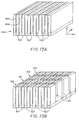
- Figs. 13A-13B show a method of making this alternative structure.
- a composite block 510 is shown similar to the block 410 in Fig. 10B.
- the block 510 includes alternating layers of thin piezoceramic wafers 501 separated along one edge by spacers 502, and then polymer layers 503 between the piezoceramic wafers 501.
- Opposing electrodes 504, 506 are on the opposing surfaces of the ceramic wafers 501.
- transverse channels 511 are cut through the composite in the x-z plane, producing a series of parallel spaced elements 512.
- channels 511 are then filled with epoxy, and one follows steps similar to those shown in Figs. 10C-10D, including lapping off of the top surface, cutting off of the bottom portion with spacers, and application of top and bottom electrodes.
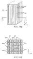
- the resulting 1-3 composite 520 is shown in Figs. 14A-14B, including a plurality of spaced elements 521 separated by polymer layers 522.
- Each element 521 includes a plurality of thin rectangular rods 524 with electrodes 525, 526 on opposing surfaces, and separated by thin rectangular rods of polymer 527.
- piezoceramic such as relaxor ferroelectric or electrostrictive materials such as lead magnesium niobate-lead titanate (PMN-PT).
- PMN-PT lead magnesium niobate-lead titanate
Landscapes
- Engineering & Computer Science (AREA)
- Mechanical Engineering (AREA)
- Chemical & Material Sciences (AREA)
- Composite Materials (AREA)
- Materials Engineering (AREA)
- Manufacturing & Machinery (AREA)
- Ultra Sonic Daignosis Equipment (AREA)
- Transducers For Ultrasonic Waves (AREA)
- Investigating Or Analyzing Materials By The Use Of Ultrasonic Waves (AREA)
Applications Claiming Priority (2)
| Application Number | Priority Date | Filing Date | Title |
|---|---|---|---|
| US292634 | 1994-08-18 | ||
| US08/292,634 US6225728B1 (en) | 1994-08-18 | 1994-08-18 | Composite piezoelectric transducer arrays with improved acoustical and electrical impedance |
Publications (2)
| Publication Number | Publication Date |
|---|---|
| EP0697257A2 true EP0697257A2 (de) | 1996-02-21 |
| EP0697257A3 EP0697257A3 (de) | 1997-07-23 |
Family
ID=23125512
Family Applications (1)
| Application Number | Title | Priority Date | Filing Date |
|---|---|---|---|
| EP95107745A Withdrawn EP0697257A3 (de) | 1994-08-18 | 1995-05-19 | Pietoelectrischer-Komposit Wandleranordnung mit verbesserter akustischer und elektrischer Impedanz |
Country Status (3)
| Country | Link |
|---|---|
| US (2) | US6225728B1 (de) |
| EP (1) | EP0697257A3 (de) |
| JP (1) | JPH08126094A (de) |
Cited By (11)
| Publication number | Priority date | Publication date | Assignee | Title |
|---|---|---|---|---|
| WO2000031808A1 (en) * | 1998-11-25 | 2000-06-02 | General Electric Company | High-sensitivity piezocomposite material and ultrasonic transducer made therefrom |
| WO2001039898A1 (en) * | 1999-12-03 | 2001-06-07 | Koninklijke Philips Electronics N.V. | Composite ultrasonic transducer array operating in the k31 mode |
| WO2001053009A1 (en) * | 2000-01-21 | 2001-07-26 | Koninklijke Philips Electronics N.V. | Hex packed two dimensional ultrasonic transducer arrays |
| GB2357213B (en) * | 1999-09-27 | 2003-01-15 | Murata Manufacturing Co | Sensor array method for manufacturing sensor array and ultrasonic diagnostic apparatus using the same |
| WO2006083539A1 (en) * | 2005-02-04 | 2006-08-10 | Siemens Medical Solutions Usa, Inc. | Multi-dimensional ultrasound transducer array |
| DE10341730B4 (de) * | 2002-09-09 | 2007-02-22 | Acuson Corp., Mountain View | Vielseitige Transducer-Array-Konfigurationen |
| EP1201322A3 (de) * | 2000-10-24 | 2009-03-18 | ATLAS ELEKTRONIK GmbH | Verfahren zur Herstellung eines Ultraschallwandlers |
| US7804228B2 (en) | 2007-12-18 | 2010-09-28 | Boston Scientific Scimed, Inc. | Composite passive materials for ultrasound transducers |
| WO2014202248A1 (de) | 2013-06-20 | 2014-12-24 | Robert Bosch Gmbh | Ultraschallwandleranordnung und kraftfahrzeug mit einer ultraschallwandleranordnung |
| CN105934835A (zh) * | 2014-02-18 | 2016-09-07 | 晶致材料科技私人有限公司 | 超宽频声波及超声波换能器 |
| EP3014898A4 (de) * | 2013-06-24 | 2017-02-22 | ZetrOZ, Inc. | Flacher, niederfrequenter und niederohmiger breitband-ultraschallwandler mit niedrigem profil, niedriger frequenz und geringer impedanz sowie verfahren dafür |
Families Citing this family (52)
| Publication number | Priority date | Publication date | Assignee | Title |
|---|---|---|---|---|
| US6278066B1 (en) * | 1996-12-20 | 2001-08-21 | Candescent Technologies Corporation | Self-standing spacer wall structures |
| US6586702B2 (en) * | 1997-09-25 | 2003-07-01 | Laser Electro Optic Application Technology Company | High density pixel array and laser micro-milling method for fabricating array |
| US7573177B2 (en) * | 1999-04-20 | 2009-08-11 | Virginia Tech Intellectual Properties, Inc. | Active/passive distributed absorber for vibration and sound radiation control |
| JP3449345B2 (ja) * | 2000-08-11 | 2003-09-22 | 株式会社村田製作所 | センサアレイおよび送受信装置 |
| US6707230B2 (en) * | 2001-05-29 | 2004-03-16 | University Of North Carolina At Charlotte | Closed loop control systems employing relaxor ferroelectric actuators |
| CN1263173C (zh) * | 2001-12-06 | 2006-07-05 | 松下电器产业株式会社 | 复合压电体及其制造方法 |
| US6821252B2 (en) * | 2002-03-26 | 2004-11-23 | G.E. Medical Systems Global Technology Company, Llc | Harmonic transducer element structures and properties |
| US6558331B1 (en) * | 2002-05-29 | 2003-05-06 | Koninklijke Philips Electronics N.V. | Apparatus and method for harmonic imaging using an array transducer operated in the k31 mode |
| US6671230B1 (en) * | 2002-06-10 | 2003-12-30 | The United States Of America As Represented By The Secretary Of The Navy | Piezoelectric volumetric array |
| US6995500B2 (en) * | 2003-07-03 | 2006-02-07 | Pathfinder Energy Services, Inc. | Composite backing layer for a downhole acoustic sensor |
| US7075215B2 (en) * | 2003-07-03 | 2006-07-11 | Pathfinder Energy Services, Inc. | Matching layer assembly for a downhole acoustic sensor |
| US7036363B2 (en) * | 2003-07-03 | 2006-05-02 | Pathfinder Energy Services, Inc. | Acoustic sensor for downhole measurement tool |
| US7513147B2 (en) * | 2003-07-03 | 2009-04-07 | Pathfinder Energy Services, Inc. | Piezocomposite transducer for a downhole measurement tool |
| US7156938B2 (en) * | 2003-11-11 | 2007-01-02 | General Electric Company | Method for making multi-layer ceramic acoustic transducer |
| US7082655B2 (en) * | 2003-12-18 | 2006-08-01 | Ge Inspection Technologies, Lp | Process for plating a piezoelectric composite |
| KR100587583B1 (ko) * | 2004-01-08 | 2006-06-08 | 학교법인 건국대학교 | 적층형 세라믹 박판 작동층을 갖는 압전세라믹의 압전작동기 구조의 제조방법 |
| US20060100522A1 (en) * | 2004-11-08 | 2006-05-11 | Scimed Life Systems, Inc. | Piezocomposite transducers |
| GB0427052D0 (en) * | 2004-12-10 | 2005-01-12 | Univ Paisley The | Ultrawideband ultrasonic transducer |
| US20070046149A1 (en) * | 2005-08-23 | 2007-03-01 | Zipparo Michael J | Ultrasound probe transducer assembly and production method |
| US7327011B2 (en) * | 2005-11-02 | 2008-02-05 | Lsi Logic Corporation | Multi-surfaced plate-to-plate capacitor and method of forming same |
| US7587936B2 (en) | 2007-02-01 | 2009-09-15 | Smith International Inc. | Apparatus and method for determining drilling fluid acoustic properties |
| US7581296B2 (en) * | 2007-04-11 | 2009-09-01 | Ge Inspection Technologies, Lp | Acoustic stack for ultrasonic transducers and method for manufacturing same |
| US7518290B2 (en) | 2007-06-19 | 2009-04-14 | Siemens Medical Solutions Usa, Inc. | Transducer array with non-uniform kerfs |
| US7750537B2 (en) * | 2007-08-16 | 2010-07-06 | University Of Virginia Patent Foundation | Hybrid dual layer diagnostic ultrasound transducer array |
| JP4412367B2 (ja) * | 2007-08-21 | 2010-02-10 | 株式会社デンソー | 超音波センサ |
| WO2009055767A2 (en) * | 2007-10-26 | 2009-04-30 | Trs Technologies, Inc. | Micromachined piezoelectric ultrasound transducer arrays |
| US8456957B2 (en) * | 2008-01-29 | 2013-06-04 | Schneider Electric USA, Inc. | Ultrasonic transducer for a proximity sensor |
| US7804742B2 (en) * | 2008-01-29 | 2010-09-28 | Hyde Park Electronics Llc | Ultrasonic transducer for a proximity sensor |
| US8117907B2 (en) | 2008-12-19 | 2012-02-21 | Pathfinder Energy Services, Inc. | Caliper logging using circumferentially spaced and/or angled transducer elements |
| JP5469344B2 (ja) * | 2009-01-14 | 2014-04-16 | 株式会社竹中工務店 | 膜型アクチュエータ、複層膜型アクチュエータ、及び空気バネ構造 |
| CA2765941A1 (en) * | 2009-06-19 | 2010-12-23 | Sonavation, Inc. | Method for manufacturing a piezoelectric ceramic body |
| WO2011083611A1 (ja) | 2010-01-06 | 2011-07-14 | テイカ株式会社 | コンポジット圧電体とそのコンポジット圧電体の製造方法およびそのコンポジット圧電体を用いたコンポジット圧電素子 |
| US8264129B2 (en) | 2010-07-21 | 2012-09-11 | General Electric Company | Device and system for measuring material thickness |
| US8680745B2 (en) | 2010-07-21 | 2014-03-25 | General Electric Company | Device for measuring material thickness |
| US9070880B2 (en) | 2010-12-23 | 2015-06-30 | Lockheed Martin Corporation | Method of manufacturing a tape cast multilayer sonar transducer |
| WO2012112137A1 (en) * | 2011-02-15 | 2012-08-23 | Halliburton Energy Services Inc. | Acoustic transducer with impedance matching layer |
| CN107398415B (zh) * | 2011-09-20 | 2020-04-21 | 新宁研究院 | 超声换能器和制造超声换能器的方法 |
| US8857261B2 (en) | 2012-04-12 | 2014-10-14 | General Electric Company | Sensing device and method of attaching the same |
| JP6102622B2 (ja) * | 2013-08-07 | 2017-03-29 | コニカミノルタ株式会社 | 超音波探触子 |
| KR20150042498A (ko) * | 2013-10-11 | 2015-04-21 | 삼성전기주식회사 | 압전소자 및 이를 포함하는 진동발생장치 |
| US10921478B2 (en) * | 2016-10-14 | 2021-02-16 | Halliburton Energy Services, Inc. | Method and transducer for acoustic logging |
| KR101830209B1 (ko) * | 2017-02-16 | 2018-02-21 | 주식회사 베프스 | 압전 센서 제조 방법 및 이를 이용한 압전 센서 |
| US11246621B2 (en) | 2018-01-29 | 2022-02-15 | Covidien Lp | Ultrasonic transducers and ultrasonic surgical instruments including the same |
| US11246617B2 (en) | 2018-01-29 | 2022-02-15 | Covidien Lp | Compact ultrasonic transducer and ultrasonic surgical instrument including the same |
| CA3107647A1 (en) * | 2018-07-31 | 2020-02-06 | Resonant Acoustics International Inc. | Ultrasonic transducer |
| RU2710103C1 (ru) * | 2018-11-30 | 2019-12-24 | федеральное государственное автономное образовательное учреждение высшего образования "Южный федеральный университет" | Способ изготовления композитного чувствительного пьезоэлемента |
| KR102807188B1 (ko) * | 2018-12-28 | 2025-05-16 | 엘지디스플레이 주식회사 | 진동발생장치, 이를 포함하는 표시장치 및 차량 |
| US11073914B2 (en) * | 2018-12-28 | 2021-07-27 | Lg Display Co., Ltd. | Vibration generation device, and display apparatus and vehicle comprising the same |
| CN109984771B (zh) * | 2019-05-06 | 2021-12-31 | 上海爱声生物医疗科技有限公司 | 一种超声换能器探头及超声成像仪 |
| CN116829352A (zh) * | 2021-01-19 | 2023-09-29 | 佐佐木贝慈 | 基板及产品 |
| CN114335324A (zh) * | 2021-12-30 | 2022-04-12 | 成都汇通西电电子有限公司 | 超声波传感器和压电复合陶瓷片及其毛坯的制备方法 |
| CN115643783B (zh) * | 2022-11-07 | 2023-07-25 | 中南大学 | 多层定向多孔压电复合材料及制备和压电能量收集器 |
Family Cites Families (22)
| Publication number | Priority date | Publication date | Assignee | Title |
|---|---|---|---|---|
| US3750243A (en) * | 1968-12-16 | 1973-08-07 | Us Navy | Low loss electrical conductive coating and bonding materials including magnetic particles for mixing |
| US3964014A (en) * | 1974-10-15 | 1976-06-15 | General Electric Company | Sonic transducer array |
| US4385255A (en) * | 1979-11-02 | 1983-05-24 | Yokogawa Electric Works, Ltd. | Linear array ultrasonic transducer |
| DE3021449A1 (de) * | 1980-06-06 | 1981-12-24 | Siemens AG, 1000 Berlin und 8000 München | Ultraschallwandleranordnung und verfahren zu seiner herstellung |
| FR2485858B1 (fr) * | 1980-06-25 | 1986-04-11 | Commissariat Energie Atomique | Procede de fabrication de transducteurs ultrasonores de formes complexes et application a l'obtention de transducteurs annulaires |
| US4514247A (en) | 1983-08-15 | 1985-04-30 | North American Philips Corporation | Method for fabricating composite transducers |
| DE3409789A1 (de) * | 1984-03-16 | 1985-09-26 | Siemens AG, 1000 Berlin und 8000 München | Piezoelektrischer luft-ultraschallwandler mit breitbandcharakteristik |
| JPH0783518B2 (ja) | 1985-10-09 | 1995-09-06 | 株式会社日立製作所 | 超音波探触子 |
| JPS62141791A (ja) * | 1985-12-16 | 1987-06-25 | Nec Corp | セラミツク変位素子 |
| JPS62179783A (ja) * | 1986-02-04 | 1987-08-06 | Olympus Optical Co Ltd | 圧電式アクチユエ−タ |
| JPS63168061A (ja) * | 1987-01-01 | 1988-07-12 | Sekisui Plastics Co Ltd | 複合圧電材料およびその製作方法 |
| US4890268A (en) * | 1988-12-27 | 1989-12-26 | General Electric Company | Two-dimensional phased array of ultrasonic transducers |
| JP2789234B2 (ja) | 1989-10-02 | 1998-08-20 | 株式会社日立メディコ | 超音波診断装置 |
| US5099459A (en) * | 1990-04-05 | 1992-03-24 | General Electric Company | Phased array ultrosonic transducer including different sized phezoelectric segments |
| JP3089851B2 (ja) * | 1992-09-16 | 2000-09-18 | 株式会社村田製作所 | チップ型圧電共振子の製造方法 |
| US5381067A (en) * | 1993-03-10 | 1995-01-10 | Hewlett-Packard Company | Electrical impedance normalization for an ultrasonic transducer array |
| US5329498A (en) * | 1993-05-17 | 1994-07-12 | Hewlett-Packard Company | Signal conditioning and interconnection for an acoustic transducer |
| JPH06332524A (ja) * | 1993-05-20 | 1994-12-02 | Fanuc Ltd | 数値制御装置における速度制御方法 |
| US5434827A (en) * | 1993-06-15 | 1995-07-18 | Hewlett-Packard Company | Matching layer for front acoustic impedance matching of clinical ultrasonic tranducers |
| US5392259A (en) * | 1993-06-15 | 1995-02-21 | Bolorforosh; Mir S. S. | Micro-grooves for the design of wideband clinical ultrasonic transducers |
| US5539965A (en) * | 1994-06-22 | 1996-07-30 | Rutgers, The University Of New Jersey | Method for making piezoelectric composites |
| US5559388A (en) * | 1995-03-03 | 1996-09-24 | General Electric Company | High density interconnect for an ultrasonic phased array and method for making |
-
1994
- 1994-08-18 US US08/292,634 patent/US6225728B1/en not_active Expired - Fee Related
-
1995
- 1995-05-19 EP EP95107745A patent/EP0697257A3/de not_active Withdrawn
- 1995-08-18 JP JP7210356A patent/JPH08126094A/ja active Pending
-
2001
- 2001-01-05 US US09/754,980 patent/US6467140B2/en not_active Expired - Fee Related
Cited By (19)
| Publication number | Priority date | Publication date | Assignee | Title |
|---|---|---|---|---|
| WO2000031808A1 (en) * | 1998-11-25 | 2000-06-02 | General Electric Company | High-sensitivity piezocomposite material and ultrasonic transducer made therefrom |
| GB2357213B (en) * | 1999-09-27 | 2003-01-15 | Murata Manufacturing Co | Sensor array method for manufacturing sensor array and ultrasonic diagnostic apparatus using the same |
| WO2001039898A1 (en) * | 1999-12-03 | 2001-06-07 | Koninklijke Philips Electronics N.V. | Composite ultrasonic transducer array operating in the k31 mode |
| WO2001053009A1 (en) * | 2000-01-21 | 2001-07-26 | Koninklijke Philips Electronics N.V. | Hex packed two dimensional ultrasonic transducer arrays |
| US6384516B1 (en) | 2000-01-21 | 2002-05-07 | Atl Ultrasound, Inc. | Hex packed two dimensional ultrasonic transducer arrays |
| US6469422B2 (en) | 2000-01-21 | 2002-10-22 | Koninklijke Philips Ultrasound N.V. | Hex packed two dimensional ultrasonic transducer arrays |
| EP1201322A3 (de) * | 2000-10-24 | 2009-03-18 | ATLAS ELEKTRONIK GmbH | Verfahren zur Herstellung eines Ultraschallwandlers |
| US7311667B2 (en) | 2002-09-09 | 2007-12-25 | Siemens Medical Solutions Usa, Inc. | Multiple pattern transducer array and method of use |
| DE10341730B4 (de) * | 2002-09-09 | 2007-02-22 | Acuson Corp., Mountain View | Vielseitige Transducer-Array-Konfigurationen |
| WO2006083539A1 (en) * | 2005-02-04 | 2006-08-10 | Siemens Medical Solutions Usa, Inc. | Multi-dimensional ultrasound transducer array |
| US7567016B2 (en) | 2005-02-04 | 2009-07-28 | Siemens Medical Solutions Usa, Inc. | Multi-dimensional ultrasound transducer array |
| US7804228B2 (en) | 2007-12-18 | 2010-09-28 | Boston Scientific Scimed, Inc. | Composite passive materials for ultrasound transducers |
| WO2014202248A1 (de) | 2013-06-20 | 2014-12-24 | Robert Bosch Gmbh | Ultraschallwandleranordnung und kraftfahrzeug mit einer ultraschallwandleranordnung |
| DE102013211612A1 (de) | 2013-06-20 | 2014-12-24 | Robert Bosch Gmbh | Ultraschallwandleranordnung und Kraftfahrzeug mit einer Ultraschallwandleranordnung |
| EP3014898A4 (de) * | 2013-06-24 | 2017-02-22 | ZetrOZ, Inc. | Flacher, niederfrequenter und niederohmiger breitband-ultraschallwandler mit niedrigem profil, niedriger frequenz und geringer impedanz sowie verfahren dafür |
| US11389832B2 (en) | 2013-06-24 | 2022-07-19 | ZetrOZ Systems, LLC | Low-profile, low-frequency, and low-impedance broad-band ultrasound transducer and methods thereof |
| CN105934835A (zh) * | 2014-02-18 | 2016-09-07 | 晶致材料科技私人有限公司 | 超宽频声波及超声波换能器 |
| EP3108511A4 (de) * | 2014-02-18 | 2017-09-06 | Microfine Materials Technologie Pte Ltd | Ultrabreitbandiger schall- und ultraschallwandler |
| CN105934835B (zh) * | 2014-02-18 | 2019-03-19 | 晶致材料科技私人有限公司 | 超宽频声波及超声波换能器 |
Also Published As
| Publication number | Publication date |
|---|---|
| JPH08126094A (ja) | 1996-05-17 |
| EP0697257A3 (de) | 1997-07-23 |
| US6467140B2 (en) | 2002-10-22 |
| US6225728B1 (en) | 2001-05-01 |
| US20010050514A1 (en) | 2001-12-13 |
Similar Documents
| Publication | Publication Date | Title |
|---|---|---|
| US6467140B2 (en) | Method of making composite piezoelectric transducer arrays | |
| US6868594B2 (en) | Method for making a transducer | |
| US5844349A (en) | Composite autoclavable ultrasonic transducers and methods of making | |
| EP0663244A2 (de) | Zwei dimensionale Akustischewandleranordnung und Verfahren zu deren Herstellung | |
| JPH0730998A (ja) | 超音波プローブ | |
| JP4933392B2 (ja) | 超音波探触子及びその製造方法 | |
| JPH05219595A (ja) | 強誘電性セラミックトランスデューサ | |
| EP0045989B1 (de) | Gerät zur akustischen Impedanzanpassung | |
| US9839411B2 (en) | Ultrasound diagnostic apparatus probe having laminated piezoelectric layers oriented at different angles | |
| US7309947B2 (en) | Piezoelectric transducer including a plurality of piezoelectric members | |
| JP2004120283A (ja) | 超音波プローブ | |
| EP1050079B1 (de) | Hochempfindliches piezoelektrisches kompositmaterial und daraus hergestellter ultraschallwandler | |
| US7876027B2 (en) | Multilayer piezoelectric and polymer ultrawideband ultrasonic transducer | |
| Mills et al. | Combining multi-layers and composites to increase SNR for medical ultrasound transducers | |
| JP2004080193A (ja) | 超音波トランスデューサおよびその製造方法 | |
| US6333590B1 (en) | Ultrasonic transducer having laminate structure, ultrasonic probe and production method thereof | |
| JPH10117399A (ja) | 超音波トランスジューサー及びその製造方法 | |
| JP2008048276A (ja) | 超音波トランスデューサ及び超音波トランスデューサアレイ | |
| JPH07194517A (ja) | 超音波探触子 | |
| Zipparo et al. | Imaging arrays with improved transmit power capability | |
| Snook et al. | Design of a high frequency annular array for medical ultrasound | |
| Bui et al. | A multifrequency composite ultrasonic transducer system | |
| JPH07108037B2 (ja) | 超音波探触子 | |
| JPH07108038B2 (ja) | 超音波探触子 | |
| Kwok et al. | Multifrequency transducers fabricated using PZT/P (VDF-TrFE) 1-3 composite |
Legal Events
| Date | Code | Title | Description |
|---|---|---|---|
| PUAI | Public reference made under article 153(3) epc to a published international application that has entered the european phase |
Free format text: ORIGINAL CODE: 0009012 |
|
| AK | Designated contracting states |
Kind code of ref document: A2 Designated state(s): DE GB NL |
|
| PUAL | Search report despatched |
Free format text: ORIGINAL CODE: 0009013 |
|
| AK | Designated contracting states |
Kind code of ref document: A3 Designated state(s): DE GB NL |
|
| STAA | Information on the status of an ep patent application or granted ep patent |
Free format text: STATUS: THE APPLICATION IS DEEMED TO BE WITHDRAWN |
|
| 18D | Application deemed to be withdrawn |
Effective date: 19980124 |