EP0697651A2 - Mikroprozessor mit Registerspeicher - Google Patents
Mikroprozessor mit Registerspeicher Download PDFInfo
- Publication number
- EP0697651A2 EP0697651A2 EP95112797A EP95112797A EP0697651A2 EP 0697651 A2 EP0697651 A2 EP 0697651A2 EP 95112797 A EP95112797 A EP 95112797A EP 95112797 A EP95112797 A EP 95112797A EP 0697651 A2 EP0697651 A2 EP 0697651A2
- Authority
- EP
- European Patent Office
- Prior art keywords
- register
- frame
- memory
- address
- designated
- Prior art date
- Legal status (The legal status is an assumption and is not a legal conclusion. Google has not performed a legal analysis and makes no representation as to the accuracy of the status listed.)
- Granted
Links
Images



Classifications
-
- G—PHYSICS
- G06—COMPUTING OR CALCULATING; COUNTING
- G06F—ELECTRIC DIGITAL DATA PROCESSING
- G06F9/00—Arrangements for program control, e.g. control units
- G06F9/06—Arrangements for program control, e.g. control units using stored programs, i.e. using an internal store of processing equipment to receive or retain programs
- G06F9/30—Arrangements for executing machine instructions, e.g. instruction decode
- G06F9/30003—Arrangements for executing specific machine instructions
- G06F9/3004—Arrangements for executing specific machine instructions to perform operations on memory
- G06F9/30043—LOAD or STORE instructions; Clear instruction
-
- G—PHYSICS
- G06—COMPUTING OR CALCULATING; COUNTING
- G06F—ELECTRIC DIGITAL DATA PROCESSING
- G06F9/00—Arrangements for program control, e.g. control units
- G06F9/06—Arrangements for program control, e.g. control units using stored programs, i.e. using an internal store of processing equipment to receive or retain programs
- G06F9/30—Arrangements for executing machine instructions, e.g. instruction decode
- G06F9/30098—Register arrangements
- G06F9/3012—Organisation of register space, e.g. banked or distributed register file
-
- G—PHYSICS
- G06—COMPUTING OR CALCULATING; COUNTING
- G06F—ELECTRIC DIGITAL DATA PROCESSING
- G06F9/00—Arrangements for program control, e.g. control units
- G06F9/06—Arrangements for program control, e.g. control units using stored programs, i.e. using an internal store of processing equipment to receive or retain programs
- G06F9/30—Arrangements for executing machine instructions, e.g. instruction decode
- G06F9/30098—Register arrangements
- G06F9/3012—Organisation of register space, e.g. banked or distributed register file
- G06F9/30123—Organisation of register space, e.g. banked or distributed register file according to context, e.g. thread buffers
- G06F9/30127—Register windows
-
- G—PHYSICS
- G06—COMPUTING OR CALCULATING; COUNTING
- G06F—ELECTRIC DIGITAL DATA PROCESSING
- G06F9/00—Arrangements for program control, e.g. control units
- G06F9/06—Arrangements for program control, e.g. control units using stored programs, i.e. using an internal store of processing equipment to receive or retain programs
- G06F9/46—Multiprogramming arrangements
- G06F9/461—Saving or restoring of program or task context
- G06F9/462—Saving or restoring of program or task context with multiple register sets
Definitions
- the present invention relates to a microprocessor, and more specifically to a microprocessor having a register file used for a high speed data access.
- a microprocessor is provided with a plurality of registers, and a programmed operation is executed in such a manner that data is loaded from a main memory to the registers, and an arithmetic and logic operation is executed using the data held in the registers, and then, the result of the operation is written into the register, and further, is written from the register to the main memory.
- the plurality of registers as mentioned above are called in a bundle a "register file".
- a register file is composed of 32 registers. This register file is small in size in comparison with a memory provided externally of the processor and a cache memory provided internally in the processor, and therefore, can be accessed with a very high speed.
- a parallel processing of a plurality of readings/writings can be realized with a relative low cost.
- the "thread” means a string of instructions obtained by sharing one process into some number of portions which are in parallel to each other or can be executed in parallel to each other.
- This "change-over of the processing between processes or threads” is called a context switching, and in the microprocessor, this context switching frequently occurs at the time of the change-over of the processes or threads and at the time of an interrupt processing.
- This execution environment may be called a "processor status", from the viewpoint of such meaning that an address is not allocated in the memory space and hardware is maintained in the microprocessor.
- the prior art has proposed a register window technique, which is adopted in the register file of a SPARC architecture which is famous as one means for a RISC (reduced instruction set computer) architecture of the microprocessor.
- the register window technique has been explained in detail in many textbooks in the field of a computer science, for example, Prentice Hall, "The SPARC Architecture Manual”, SPARC International, Inc., Chapter 4, the disclosure of which is incorporated by reference in its entirety into the present application.
- Figure 1 illustrates a plurality of register windows included in the register file.
- the register file is divided into N register windows including a register window 6011, a register window 6012, a register window 6013, ⁇ ⁇ ⁇ , a register window 601 (N-1) , and a register window 601 N . These register windows partially overlap each other.
- the hatched portion shows an overlapping portion of each pair of adjacent register windows
- the register window technique has been developed in order to speed up the function calling
- the register window technique may be used in order to speed up the context switching, for example by allocating each window to each process or thread.
- the saving and restoring of the content of the register in response to the context switching is no longer necessary. In this case, however, it is not possible to use the overlap between the register windows.
- the register file is indispensable in elevating the performance of the microprocessor.
- the content of the register file must be saved into the memory, resulting in the generation of a large overhead.
- This overhead becomes a serious problem in an application environment in which the context switching occurs frequently. This becomes a hindrance in working, for example, in embedded system in which a microprocessor is used for control an external instrument, or in a parallel processor system using a plurality of microprocessors.
- the conventional register window if the number of register windows provided in the register file is sufficient, it is advantageous since it is not necessary to save the content of the registers. In addition, it is possible to speed up the context switching. However, if the number of register windows becomes short or insufficient, it becomes necessary for the operating system to intervene so as to save the content of the overflowing register window into the memory. In this case, there is required a processing time longer than that required when the context switching occurs in the conventional register file.
- Another object of the present invention is to provide a microprocessor having a new register file which can realize a high speed, more flexible, context switching.
- a microprocessor including at least a register file and an instruction pipeline and so configured that a data load/store processing is performed between the register file and an external memory
- the register file comprising: a plurality of register banks each composed of the same number of registers; a plurality of frame address storing registers of the same number as that of the plurality of register banks; a first data read/write means connected to the instruction pipeline through a register designating bus means and a first data transfer bus means and also coupled to the plurality of register banks; an address read/write means connected to the instruction pipeline through an address transfer bus means and coupled to the plurality of frame address storing registers; and a second data read/write means coupled to the plurality of register banks and connected to the memory through a second data transfer bus means.
- the microprocessor further includes a plurality of frame status storing registers of the same number as that of the plurality of register banks, and a frame status update means connected to the instruction pipeline through a frame status transfer line means and coupled to the plurality of frame status storing registers.
- the microprocessor further includes a plurality of register bank number storing registers of the same number as that of the plurality of register banks, and a register bank selection means connected to the instruction pipeline through a register designating line means and coupled to the plurality of register bank number storing registers.
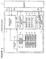
- FIG. 2 there is shown a block diagram of a first embodiment of the microprocessor in accordance with the present invention.
- the shown microprocessor is generally designated by Reference Numeral 1, and is coupled to a memory 2.
- the microprocessor 1 includes an instruction pipeline 3 and a register file 4.
- the register file 4 includes an address read/write circuit 5, a plurality of frame address storing registers 6 coupled to the address read/write circuit 5, data read/write circuits 7 and 10, and register banks 8 of the same number as that of the frame address storing registers 6.
- the register banks 8 are coupled to the data read/write circuits 7 and 10, and all the register banks 8 are composed of the same number of registers 9.
- the instruction pipeline 3 is coupled to the register file 4 through a register designating bus 104, a data transfer bus 105, and an address transfer bus 106.
- the instruction pipeline 3 is also coupled to the memory 2 through a memory address bus 101 and an instruction supply bus 102, and the data read/write circuit 10 is coupled to the memory 2 through a data transfer bus 103.
- the instruction pipeline 3 is in charge of an internal sequential processing executed in a pipelined fashion in accordance with instructions described in a program.
- the instruction pipeline 3 designates through the memory address bus 101 an address within the memory 2, so that an instruction stored in the designated address is read out from the memory 2 and supplied through the instruction supplying bus 102 to the instruction pipeline 3.
- a processing designated by the read-out instruction is executed.
- the designated processing is executed, if data stored in a register 9 in the register banks 8 of the register file 4 is required, or if the result of the processing is to be stored in a register 9 in the register banks 8, the register 9 in the register file 4 is accessed.
- a load/store instruction of data not greater than one word is processed, data is transferred between one register 9 and the memory 2 through the data transfer bus 103 and the data read/write circuit 10.
- the address for the memory 2 is supplied from the instruction pipeline 3 through the memory address bus 101 to the memory 2.
- the "word" indicates the size or the bit number of data stored in one register 9.
- the "frame” is defined to mean data of the same bit number as that of one register bank 8.
- the "frame address” means an address in the memory 2 given to this frame.
- the frame address is designated through the memory address bus 101 by the instruction pipeline 3, so that the frame stored at a location indicated by the designated frame address is written into the register bank 8 through the data transfer bus 103 and the data read/write circuit 10. Which of the register banks 8 should be written, is designated from the instruction pipeline 3 through the register designating bus 104 and the data read/write circuit 7. In addition, the designated frame address is written into the frame address storing register 6 corresponding to the designated register bank 8, through the address transfer bus 106 and the address read/write circuit 5.
- the processing of the frame storing instruction can be performed in two ways.
- the first storing way from which of the register banks 8 the frame is to be stored in the memory 2, is designated through the register designating bus 104 by the instruction pipeline 3.
- the frame address stored in the frame address storing register 6 corresponding to the designated register bank 8 is used as the frame address indicating a storing location of the memory 2.
- This frame address is read out by the address read/write circuit 5 and supplied through the address transfer bus 106 to the instruction pipeline 3, so as to be further supplied through the memory address bus 101 to the memory 2.
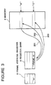
- FIG. 3 there are illustrated the frame address designating ways when an instruction for loading/storing data in units of frame is executed in the first embodiment shown in Figure 2.
- the frame address "A" is designated. As shown in the operation line 201, the frame stored at a location in the memory 2 designated by the frame address "A”, is read out from the memory 2, and stored into the designated register bank 8. In addition, the frame address "A" is stored into the corresponding frame address storing register 6.
- the frame In order to store this frame in the above mentioned first way, as shown in the operation line 202, the frame is stored in the read-out original location of the memory 2. On the other hand, in order to store this frame in the above mentioned second way, as shown in the operation line 203, the frame "A" is stored into a location in the memory 2 designated by the frame address "C", regardless of from where in the memory the frame is read out for loading into the register file.
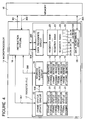
- FIG. 4 is a block diagram of a second embodiment of the microprocessor in accordance with the present invention.
- the microprocessor of the second embodiment is generally designated by Reference Numeral 14, and is coupled to a memory 15.
- the microprocessor 14 includes an instruction pipeline 16 and a register file 17.
- the register file 17 includes an address read/write circuit 18, a plurality of frame address storing registers 19 coupled to the address read/write circuit 18, a frame status update circuit 20, frame status storing registers 21 of the same number as that of the frame address storing registers 19, data read/write circuits 22 and 25, and register banks 23 of the same number as that of the frame address storing registers 19.
- the frame status storing registers 21 is coupled to the frame status update circuit 20.
- the register banks 23 is coupled to the data read/write circuits 22 and 25, and all the register banks 23 are composed of the same number of registers 24.
- the instruction pipeline 16 is coupled to the register file 17 through a register designating bus 304, a data transfer bus 305, an address transfer bus 306, and a frame status transfer bus 307.
- the address read/write circuit 18 is coupled to the frame status update circuit 20 through a frame save control line 308.
- the instruction pipeline 16 is also coupled to the memory 15 through a memory address bus 301 and an instruction supply bus 302, and the data read/write circuit 25 is coupled to the memory 15 through a data transfer bus 303.
- the newly added frame status storing registers 21 stores information indicating whether or not the frame stored in a corresponding register bank 23 is valid.
- Figure 5 is a status transition diagram between the frame validation and the frame invalidation in the second embodiment shown in Figure 4.
- legends (1), (2) and (A) added to arrowhead curved status transition lines indicate an event which cause any status transition.
- the status transition (1) shows to load a frame into a corresponding register bank 23, and the status transition (2) shows to write into a register 24 in the register bank 23.
- the status transition (A) shows to store the frame in accordance with the above mentioned second way.
- the valid status is maintained as it is as shown by the transition line 402.
- the invalid status is maintained as it is as shown by the transition line 404, and the newly loaded frame is overwritten onto the invalid frame (403).
- FIG. 6 there is shown a block diagram of a third embodiment of the microprocessor in accordance with the present invention.
- the microprocessor of the third embodiment is generally designated by Reference Numeral 26, and is coupled to a memory 27.
- the microprocessor 26 includes an instruction pipeline 28 and a register file 29.
- the register file 29 includes an address read/write circuit 30, a plurality of frame address storing registers 31 coupled to the address read/write circuit 30, a frame status update circuit 32, frame status storing registers 33 which are of the same number as that of the frame address storing registers 31 and which are coupled to the frame status update circuit 32, data read/write circuits 34 and 37, register banks 35 which are of the same number as that of the frame address storing registers 31 and which are coupled to data read/write circuits 34 and 37, a register bank selection circuit 38, and register bank number registers 39 which are of the same number as that of the frame address storing registers 31 and which are coupled to the register bank selection circuit 38. All the register banks 35 are composed of the same number of registers 36.
- the instruction pipeline 28 is coupled to the register file 29 through a data transfer bus 505, an address transfer bus 506, a frame status transfer bus 507 and a register designating bus 509.
- the address read/write circuit 30 is coupled to the frame status update circuit 32 through a frame save control line 508.
- the instruction pipeline 28 is also coupled to the memory 27 through a memory address bus 501 and an instruction supply bus 502, and the data read/write circuit 37 is coupled to the memory 27 through a data transfer bus 503.
- this third embodiment is characterized by newly comprising the register bank selection circuit 38 and the plurality of register bank number registers 39.
- the number of the register banks 8 and 23 in the register files 4 and 17 is limited by the size of register set, but in this third embodiment, the number of the register banks 35 can be freely set.
- the "size of register set" means the number of registers which can be designated from an instruction of a processor.
- this third embodiment can set the number of register banks 35 to the effect that the number of the registers 35 within the register file 29 is larger than the size of register set.
- each of the register bank number registers 39 associated to the register banks 35 stores the register bank number indicating to which register bank in the register set the associated register bank 35 corresponds.
- each of the register banks 35 is composed of eight registers, and the "size of register set" is 32 registers.
- the register set is constituted of four banks, namely, bank "0" to bank "3". Therefore, the register bank number can take four values from "0" to "3".
- the register bank number in the register set is stored in the register bank number register 39, so that the register bank 35 is indirectly accessed.
- the register hank selection circuit 38 compares the register 36 or the register bank 35 designated by the instruction pipeline 28 through the register designating bus 509, with the register bank number stored in the register bank number registers 39, and if coincidence is obtained, the coincident register bank 35 is accessed.
- the register bank 35 storing an invalid frame is selected by the register bank selection circuit 38, and the frame is stored in the selected register bank 35.
- the register bank number of the loaded destination is stored in the register bank number register 39 corresponding to the register bark 35 loaded with the frame, and also, the frame address of the loaded frame is stored in the corresponding frame address storing register 31.
- the status of the corresponding frame state storing register 33 is changed in accordance with the status transition procedure explained in connection with the second embodiment.
- the register bank selection circuit 38 determines or selects which of the invalid register banks should be loaded with the frame. For example, it can be considered to select in accordance with an algorithm such as an LRU (Least Recently Used) algorithm.
- LRU Least Recently Used
- the present invention is characterized in that the address in the memory space is given to the data stored in the registers and held in the register file. With this arrangement, it is no longer necessary to save the data stored in the registers, into the memory space of the operating system. Instead, the data can be automatically saved to a location of a given address by means of hardware if necessary. Thins, it is possible to avoid the drop of the processing speed at the time of the context switching.
- the register bark number register is associated to each of the register banks, so that the register bank number in the register set is stored in the register bank number register.
- the register file in accordance with the present invention is such that each frame has the frame address in the memory. Accordingly, it is possible to store the frame into the memory by means of the hardware means. Thus, when an overflow occurs in the register file, the time required for processing the overflow can be shortened. Similarly, it is possible to further speed up the processing speed at the time of the context switching.
Landscapes
- Engineering & Computer Science (AREA)
- Software Systems (AREA)
- Theoretical Computer Science (AREA)
- Physics & Mathematics (AREA)
- General Engineering & Computer Science (AREA)
- General Physics & Mathematics (AREA)
- Executing Machine-Instructions (AREA)
- Microcomputers (AREA)
Applications Claiming Priority (3)
| Application Number | Priority Date | Filing Date | Title |
|---|---|---|---|
| JP190447/94 | 1994-08-12 | ||
| JP19044794 | 1994-08-12 | ||
| JP6190447A JP2677202B2 (ja) | 1994-08-12 | 1994-08-12 | マイクロプロセッサ |
Publications (3)
| Publication Number | Publication Date |
|---|---|
| EP0697651A2 true EP0697651A2 (de) | 1996-02-21 |
| EP0697651A3 EP0697651A3 (de) | 1997-07-23 |
| EP0697651B1 EP0697651B1 (de) | 2001-11-07 |
Family
ID=16258290
Family Applications (1)
| Application Number | Title | Priority Date | Filing Date |
|---|---|---|---|
| EP95112797A Expired - Lifetime EP0697651B1 (de) | 1994-08-12 | 1995-08-14 | Mikroprozessor mit Registerspeicher |
Country Status (4)
| Country | Link |
|---|---|
| US (1) | US5713038A (de) |
| EP (1) | EP0697651B1 (de) |
| JP (1) | JP2677202B2 (de) |
| DE (1) | DE69523690T2 (de) |
Cited By (1)
| Publication number | Priority date | Publication date | Assignee | Title |
|---|---|---|---|---|
| WO2001029664A3 (en) * | 1999-10-20 | 2002-06-06 | Sony Electronics Inc | Method for utilizing concurrent context switching to support isochronous processes |
Families Citing this family (26)
| Publication number | Priority date | Publication date | Assignee | Title |
|---|---|---|---|---|
| US5778243A (en) * | 1996-07-03 | 1998-07-07 | International Business Machines Corporation | Multi-threaded cell for a memory |
| US6223208B1 (en) * | 1997-10-03 | 2001-04-24 | International Business Machines Corporation | Moving data in and out of processor units using idle register/storage functional units |
| US6145049A (en) * | 1997-12-29 | 2000-11-07 | Stmicroelectronics, Inc. | Method and apparatus for providing fast switching between floating point and multimedia instructions using any combination of a first register file set and a second register file set |
| US7444641B1 (en) * | 1998-03-10 | 2008-10-28 | Agere Systems Inc. | Context controller having context-specific event selection mechanism and processor employing the same |
| US6986141B1 (en) * | 1998-03-10 | 2006-01-10 | Agere Systems Inc. | Context controller having instruction-based time slice task switching capability and processor employing the same |
| US7035997B1 (en) | 1998-12-16 | 2006-04-25 | Mips Technologies, Inc. | Methods and apparatus for improving fetching and dispatch of instructions in multithreaded processors |
| US6389449B1 (en) * | 1998-12-16 | 2002-05-14 | Clearwater Networks, Inc. | Interstream control and communications for multi-streaming digital processors |
| US7257814B1 (en) | 1998-12-16 | 2007-08-14 | Mips Technologies, Inc. | Method and apparatus for implementing atomicity of memory operations in dynamic multi-streaming processors |
| US7529907B2 (en) | 1998-12-16 | 2009-05-05 | Mips Technologies, Inc. | Method and apparatus for improved computer load and store operations |
| US7020879B1 (en) * | 1998-12-16 | 2006-03-28 | Mips Technologies, Inc. | Interrupt and exception handling for multi-streaming digital processors |
| US7237093B1 (en) | 1998-12-16 | 2007-06-26 | Mips Technologies, Inc. | Instruction fetching system in a multithreaded processor utilizing cache miss predictions to fetch instructions from multiple hardware streams |
| US6292888B1 (en) * | 1999-01-27 | 2001-09-18 | Clearwater Networks, Inc. | Register transfer unit for electronic processor |
| US6487630B2 (en) * | 1999-02-26 | 2002-11-26 | Intel Corporation | Processor with register stack engine that dynamically spills/fills physical registers to backing store |
| US6507862B1 (en) * | 1999-05-11 | 2003-01-14 | Sun Microsystems, Inc. | Switching method in a multi-threaded processor |
| US6351808B1 (en) * | 1999-05-11 | 2002-02-26 | Sun Microsystems, Inc. | Vertically and horizontally threaded processor with multidimensional storage for storing thread data |
| US6668285B1 (en) | 1999-05-12 | 2003-12-23 | Koninklijke Philips Electronics N.V. | Object oriented processing with dedicated pointer memories |
| DE60143896D1 (de) | 2000-07-14 | 2011-03-03 | Mips Tech Inc | Anweisungsabruf und -absendung in einem multi-thread-system |
| KR100491323B1 (ko) * | 2002-03-13 | 2005-05-24 | (주) 네오시스트 | 독립 파이프라인에 의한 저장 방식을 갖는 전자 계산기 |
| JP2005284646A (ja) | 2004-03-29 | 2005-10-13 | Toshiba Corp | マイクロプロセッサ |
| JP2006092042A (ja) * | 2004-09-21 | 2006-04-06 | Sanyo Electric Co Ltd | 情報処理装置及びコンテキスト切り替え方法 |
| EP2056198A4 (de) | 2006-08-24 | 2010-08-18 | Netcleus Systems Corp | Task-verarbeitungseinrichtung |
| US8938590B2 (en) | 2008-10-18 | 2015-01-20 | Micron Technology, Inc. | Indirect register access method and system |
| US8209521B2 (en) * | 2008-10-18 | 2012-06-26 | Micron Technology, Inc. | Methods of indirect register access including automatic modification of a directly accessible address register |
| GB2605665B (en) | 2021-09-30 | 2023-11-01 | Imagination Tech Ltd | Graphics processor |
| GB2605471B (en) | 2021-09-30 | 2023-11-01 | Imagination Tech Ltd | Processor with hardware pipeline |
| GB2605664B (en) * | 2021-09-30 | 2023-03-29 | Imagination Tech Ltd | Processor with hardware pipeline |
Family Cites Families (11)
| Publication number | Priority date | Publication date | Assignee | Title |
|---|---|---|---|---|
| US4627024A (en) * | 1983-07-21 | 1986-12-02 | Trw Inc. | Window-addressable memory circuit |
| JPS6151243A (ja) * | 1984-08-20 | 1986-03-13 | Toshiba Corp | レジスタ式演算処理装置 |
| JPS63156236A (ja) * | 1986-12-19 | 1988-06-29 | Toshiba Corp | レジスタ装置 |
| JPH0769821B2 (ja) * | 1988-03-04 | 1995-07-31 | 日本電気株式会社 | 情報処理装置におけるバイパスライン制御方式 |
| JP2655191B2 (ja) * | 1989-07-05 | 1997-09-17 | 三菱電機株式会社 | 演算処理装置 |
| JPH0454652A (ja) * | 1990-06-25 | 1992-02-21 | Nec Corp | マイクロコンピュータ |
| US5226142A (en) * | 1990-11-21 | 1993-07-06 | Ross Technology, Inc. | High performance register file with overlapping windows |
| KR960001273B1 (ko) * | 1991-04-30 | 1996-01-25 | 가부시키가이샤 도시바 | 단일칩 마이크로컴퓨터 |
| US5557766A (en) * | 1991-10-21 | 1996-09-17 | Kabushiki Kaisha Toshiba | High-speed processor for handling multiple interrupts utilizing an exclusive-use bus and current and previous bank pointers to specify a return bank |
| JP2568017B2 (ja) * | 1992-03-12 | 1996-12-25 | 株式会社東芝 | マイクロプロセッサ及びそれを使用したデータ処理システム |
| JP3110866B2 (ja) * | 1992-06-01 | 2000-11-20 | 株式会社東芝 | マイクロプロセッサ |
-
1994
- 1994-08-12 JP JP6190447A patent/JP2677202B2/ja not_active Expired - Fee Related
-
1995
- 1995-08-14 EP EP95112797A patent/EP0697651B1/de not_active Expired - Lifetime
- 1995-08-14 US US08/514,928 patent/US5713038A/en not_active Expired - Fee Related
- 1995-08-14 DE DE69523690T patent/DE69523690T2/de not_active Expired - Lifetime
Non-Patent Citations (1)
| Title |
|---|
| A. SILBERSCHATZ, J. PETERSON AND P. GALVIN: "Operating System Concepts", ADDISON-WESLEY PUBLISHING COMPANY, pages: 106 |
Cited By (2)
| Publication number | Priority date | Publication date | Assignee | Title |
|---|---|---|---|---|
| WO2001029664A3 (en) * | 1999-10-20 | 2002-06-06 | Sony Electronics Inc | Method for utilizing concurrent context switching to support isochronous processes |
| US7318090B1 (en) | 1999-10-20 | 2008-01-08 | Sony Corporation | Method for utilizing concurrent context switching to support isochronous processes |
Also Published As
| Publication number | Publication date |
|---|---|
| EP0697651A3 (de) | 1997-07-23 |
| US5713038A (en) | 1998-01-27 |
| JP2677202B2 (ja) | 1997-11-17 |
| DE69523690T2 (de) | 2002-08-01 |
| JPH0855028A (ja) | 1996-02-27 |
| EP0697651B1 (de) | 2001-11-07 |
| DE69523690D1 (de) | 2001-12-13 |
Similar Documents
| Publication | Publication Date | Title |
|---|---|---|
| US5713038A (en) | Microprocessor having register file | |
| US6131145A (en) | Information processing unit and method for controlling a hierarchical cache utilizing indicator bits to control content of prefetching operations | |
| US5809274A (en) | Purge control for ON-chip cache memory | |
| US5590379A (en) | Method and apparatus for cache memory access with separate fetch and store queues | |
| EP0409415A2 (de) | Schnelle Mehrwortzugänglichkeit aus einem Mehrwegset-assoziativen Cache-Speicher | |
| JPS6136667B2 (de) | ||
| US20020116581A1 (en) | Memory aliasing in a processor system | |
| US20040139277A1 (en) | Cache memory, processor and cache control method | |
| JP2523814B2 (ja) | ム―ブアウト・システム | |
| US8266379B2 (en) | Multithreaded processor with multiple caches | |
| JP2003196086A (ja) | レジスタウィンドウ方式によるレジスタファイル及びその制御方法 | |
| US5729723A (en) | Data processing unit | |
| US5179682A (en) | Method and apparatus for improved current window cache with switchable address in, out, and local cache registers | |
| US5933856A (en) | System and method for processing of memory data and communication system comprising such system | |
| JP2004110240A (ja) | キャッシュメモリ装置 | |
| KR960012354B1 (ko) | 마이크로 프로세서 | |
| EP1278121A2 (de) | Mikroprozessor mit Aufrechterhaltung der Speicherübereinstimmung | |
| US5349672A (en) | Data processor having logical address memories and purge capabilities | |
| JPS6051947A (ja) | 仮想記憶計算機における命令先取方式 | |
| EP1139214A1 (de) | Anordnung und Verfahren, die es ermöglichen, einen Zweiwortbefehl in einem einzelnen Zyklus durchzuführen | |
| JPH044630B2 (de) | ||
| JPH0666052B2 (ja) | メモリ内容を機械レジスタに自動的に写像する計算機 | |
| JPH1055308A (ja) | キャッシュメモリ | |
| EP0634717B1 (de) | Datenverarbeitungseinheit | |
| WO2012077516A1 (ja) | プログラマブルコントローラ |
Legal Events
| Date | Code | Title | Description |
|---|---|---|---|
| PUAI | Public reference made under article 153(3) epc to a published international application that has entered the european phase |
Free format text: ORIGINAL CODE: 0009012 |
|
| AK | Designated contracting states |
Kind code of ref document: A2 Designated state(s): DE FR GB |
|
| PUAL | Search report despatched |
Free format text: ORIGINAL CODE: 0009013 |
|
| AK | Designated contracting states |
Kind code of ref document: A3 Designated state(s): DE FR GB |
|
| 17P | Request for examination filed |
Effective date: 19971105 |
|
| 17Q | First examination report despatched |
Effective date: 19991011 |
|
| GRAG | Despatch of communication of intention to grant |
Free format text: ORIGINAL CODE: EPIDOS AGRA |
|
| GRAG | Despatch of communication of intention to grant |
Free format text: ORIGINAL CODE: EPIDOS AGRA |
|
| GRAH | Despatch of communication of intention to grant a patent |
Free format text: ORIGINAL CODE: EPIDOS IGRA |
|
| GRAH | Despatch of communication of intention to grant a patent |
Free format text: ORIGINAL CODE: EPIDOS IGRA |
|
| GRAA | (expected) grant |
Free format text: ORIGINAL CODE: 0009210 |
|
| AK | Designated contracting states |
Kind code of ref document: B1 Designated state(s): DE FR GB |
|
| REF | Corresponds to: |
Ref document number: 69523690 Country of ref document: DE Date of ref document: 20011213 |
|
| REG | Reference to a national code |
Ref country code: GB Ref legal event code: IF02 |
|
| ET | Fr: translation filed | ||
| PLBE | No opposition filed within time limit |
Free format text: ORIGINAL CODE: 0009261 |
|
| STAA | Information on the status of an ep patent application or granted ep patent |
Free format text: STATUS: NO OPPOSITION FILED WITHIN TIME LIMIT |
|
| 26N | No opposition filed | ||
| PGFP | Annual fee paid to national office [announced via postgrant information from national office to epo] |
Ref country code: DE Payment date: 20130807 Year of fee payment: 19 |
|
| PGFP | Annual fee paid to national office [announced via postgrant information from national office to epo] |
Ref country code: FR Payment date: 20130808 Year of fee payment: 19 Ref country code: GB Payment date: 20130814 Year of fee payment: 19 |
|
| REG | Reference to a national code |
Ref country code: DE Ref legal event code: R119 Ref document number: 69523690 Country of ref document: DE |
|
| GBPC | Gb: european patent ceased through non-payment of renewal fee |
Effective date: 20140814 |
|
| REG | Reference to a national code |
Ref country code: DE Ref legal event code: R119 Ref document number: 69523690 Country of ref document: DE Effective date: 20150303 |
|
| REG | Reference to a national code |
Ref country code: FR Ref legal event code: ST Effective date: 20150430 |
|
| PG25 | Lapsed in a contracting state [announced via postgrant information from national office to epo] |
Ref country code: DE Free format text: LAPSE BECAUSE OF NON-PAYMENT OF DUE FEES Effective date: 20150303 Ref country code: GB Free format text: LAPSE BECAUSE OF NON-PAYMENT OF DUE FEES Effective date: 20140814 |
|
| PG25 | Lapsed in a contracting state [announced via postgrant information from national office to epo] |
Ref country code: FR Free format text: LAPSE BECAUSE OF NON-PAYMENT OF DUE FEES Effective date: 20140901 |