EP0697768B1 - Eine kalibrierte Impulsbreite erzeugender Detektor für den Übergang eines Logiksignals - Google Patents
Eine kalibrierte Impulsbreite erzeugender Detektor für den Übergang eines Logiksignals Download PDFInfo
- Publication number
- EP0697768B1 EP0697768B1 EP95401893A EP95401893A EP0697768B1 EP 0697768 B1 EP0697768 B1 EP 0697768B1 EP 95401893 A EP95401893 A EP 95401893A EP 95401893 A EP95401893 A EP 95401893A EP 0697768 B1 EP0697768 B1 EP 0697768B1
- Authority
- EP
- European Patent Office
- Prior art keywords
- signal
- phase
- delay
- delay circuit
- auxiliary
- Prior art date
- Legal status (The legal status is an assumption and is not a legal conclusion. Google has not performed a legal analysis and makes no representation as to the accuracy of the status listed.)
- Expired - Lifetime
Links
- 230000007704 transition Effects 0.000 title claims description 36
- 238000001514 detection method Methods 0.000 claims description 10
- 230000010363 phase shift Effects 0.000 claims description 4
- 230000001360 synchronised effect Effects 0.000 claims description 3
- 238000007493 shaping process Methods 0.000 description 8
- 230000000630 rising effect Effects 0.000 description 7
- 238000010586 diagram Methods 0.000 description 6
- 235000021183 entrée Nutrition 0.000 description 6
- 230000010354 integration Effects 0.000 description 4
- 230000005540 biological transmission Effects 0.000 description 3
- 230000008901 benefit Effects 0.000 description 2
- 239000000470 constituent Substances 0.000 description 2
- 238000012937 correction Methods 0.000 description 2
- 230000003247 decreasing effect Effects 0.000 description 2
- 238000005516 engineering process Methods 0.000 description 2
- 230000006870 function Effects 0.000 description 2
- 230000004048 modification Effects 0.000 description 2
- 238000012986 modification Methods 0.000 description 2
- 239000010453 quartz Substances 0.000 description 2
- VYPSYNLAJGMNEJ-UHFFFAOYSA-N silicon dioxide Inorganic materials O=[Si]=O VYPSYNLAJGMNEJ-UHFFFAOYSA-N 0.000 description 2
- 238000012360 testing method Methods 0.000 description 2
- 241001644893 Entandrophragma utile Species 0.000 description 1
- 241001080024 Telles Species 0.000 description 1
- 230000008859 change Effects 0.000 description 1
- 125000004122 cyclic group Chemical group 0.000 description 1
- 230000001934 delay Effects 0.000 description 1
- 230000003111 delayed effect Effects 0.000 description 1
- 230000001419 dependent effect Effects 0.000 description 1
- 238000007599 discharging Methods 0.000 description 1
- 238000000605 extraction Methods 0.000 description 1
- 230000000670 limiting effect Effects 0.000 description 1
- 238000004519 manufacturing process Methods 0.000 description 1
- 230000000873 masking effect Effects 0.000 description 1
- 238000005259 measurement Methods 0.000 description 1
- 230000015654 memory Effects 0.000 description 1
- 238000000034 method Methods 0.000 description 1
- 238000010587 phase diagram Methods 0.000 description 1
- 238000011084 recovery Methods 0.000 description 1
- 230000002829 reductive effect Effects 0.000 description 1
- 239000013643 reference control Substances 0.000 description 1
- 230000003068 static effect Effects 0.000 description 1
- 238000011144 upstream manufacturing Methods 0.000 description 1
Images



Classifications
-
- H—ELECTRICITY
- H03—ELECTRONIC CIRCUITRY
- H03L—AUTOMATIC CONTROL, STARTING, SYNCHRONISATION OR STABILISATION OF GENERATORS OF ELECTRONIC OSCILLATIONS OR PULSES
- H03L7/00—Automatic control of frequency or phase; Synchronisation
- H03L7/06—Automatic control of frequency or phase; Synchronisation using a reference signal applied to a frequency- or phase-locked loop
- H03L7/08—Details of the phase-locked loop
- H03L7/0805—Details of the phase-locked loop the loop being adapted to provide an additional control signal for use outside the loop
-
- H—ELECTRICITY
- H03—ELECTRONIC CIRCUITRY
- H03K—PULSE TECHNIQUE
- H03K5/00—Manipulating of pulses not covered by one of the other main groups of this subclass
- H03K5/153—Arrangements in which a pulse is delivered at the instant when a predetermined characteristic of an input signal is present or at a fixed time interval after this instant
- H03K5/1534—Transition or edge detectors
-
- H—ELECTRICITY
- H03—ELECTRONIC CIRCUITRY
- H03L—AUTOMATIC CONTROL, STARTING, SYNCHRONISATION OR STABILISATION OF GENERATORS OF ELECTRONIC OSCILLATIONS OR PULSES
- H03L7/00—Automatic control of frequency or phase; Synchronisation
- H03L7/06—Automatic control of frequency or phase; Synchronisation using a reference signal applied to a frequency- or phase-locked loop
- H03L7/08—Details of the phase-locked loop
- H03L7/081—Details of the phase-locked loop provided with an additional controlled phase shifter
- H03L7/0812—Details of the phase-locked loop provided with an additional controlled phase shifter and where no voltage or current controlled oscillator is used
- H03L7/0816—Details of the phase-locked loop provided with an additional controlled phase shifter and where no voltage or current controlled oscillator is used the controlled phase shifter and the frequency- or phase-detection arrangement being connected to a common input
-
- H—ELECTRICITY
- H04—ELECTRIC COMMUNICATION TECHNIQUE
- H04L—TRANSMISSION OF DIGITAL INFORMATION, e.g. TELEGRAPHIC COMMUNICATION
- H04L7/00—Arrangements for synchronising receiver with transmitter
- H04L7/02—Speed or phase control by the received code signals, the signals containing no special synchronisation information
- H04L7/033—Speed or phase control by the received code signals, the signals containing no special synchronisation information using the transitions of the received signal to control the phase of the synchronising-signal-generating means, e.g. using a phase-locked loop
-
- H—ELECTRICITY
- H04—ELECTRIC COMMUNICATION TECHNIQUE
- H04L—TRANSMISSION OF DIGITAL INFORMATION, e.g. TELEGRAPHIC COMMUNICATION
- H04L7/00—Arrangements for synchronising receiver with transmitter
- H04L7/0079—Receiver details
- H04L7/0087—Preprocessing of received signal for synchronisation, e.g. by code conversion, pulse generation or edge detection
Definitions
- the invention relates to a transition detector. of a logic signal generating a duration pulse calibrated.
- a known solution as described for example in the document DE 4 326 134 A, consists, according to a conventional diagram, as shown in FIG. 1, of using an exclusive OR logic gate with two inputs, each supplied directly respectively via a delay line by the signal whose transition must be detected.
- the exclusive OR logic gate on the appearance of the transition, delivers a pulse the duration of which is equal to the duration of the delay introduced by the delay line on the input signal.
- an analog type delay line is used, or elementary logic circuits or gates each introducing an elementary propagation delay.
- the delay introduced is very stable, over a wide range of operating conditions.
- this type of component cannot be integrated, and must therefore be introduced as an external element.
- the duration of the delay introduced is very dependent on variations in the operating conditions, such as the temperature for example.
- the main advantage in the aforementioned second case is that this type of circuit can be perfectly integrated.
- Document US 4,789,976 describes a device for delay compensation due to temperature in a system of video disc rotation control.
- the device includes a delay compensation circuit in which a ring oscillator 20 and a quartz oscillator 32 are used. Due to the presence of these two elements, the compensation system is complex to implement and therefore more expensive.
- EP-A-0 392 653 describes a system clock extraction using a logic gate AND or NON-AND type and a delay line controlled by synchronization by a phase loop fitted with a ring oscillator, which ensures this synchronization on the edges of a clock signal.
- a logic gate AND or NON-AND type used for masking the pulses of data.
- the object of the present invention is to remedy the aforementioned drawbacks.
- the transition detector of a logic signal, object of the present invention includes a logic gate Exclusive OR whose first input receives this signal logic via a specific delay circuit.
- auxiliary delay circuit associated with the delay circuit by a phase locked loop, which allows to generate, from a frequency signal of reference, a common phase control signal allowing to control the delay brought by the delay circuit and by the auxiliary delay circuit to a value proportional to the period of the frequency signal reference, which generates, for each transition of the logic signal, a calibrated pulse of which the duration is proportional to the period of the signal reference frequency.
- the transition detector object of the present invention, finds particular application to the realization of electronic memories in the form of integrated circuits.
- the signal transition detector logic object of the present invention includes a door logic of exclusive OR type, referenced 1, a first of which input receives the logic signal, noted Ven, on which the transition must be detected and including a second entry receives this same logic signal via a determined delay circuit, referenced 2.
- the transition detector comprises an auxiliary delay circuit, noted 30, associated with delay circuit 2 via a phase locked loop, referenced 3.
- the phase-locked loop 3 generates, at from a reference frequency signal whose ratio cyclic is preferably equal to 1/2, denoted CLK, a signal phase control, denoted V0, common to the delay circuit determined 2 and at the auxiliary delay circuit 30 and allowing to control the delay brought by the circuit of delay 2 and by the auxiliary delay circuit 30 at one value proportional to the period of the frequency signal CLK reference.
- the delay generated by delay circuit 2 is thus fixed, which allows to generate at the output of the exclusive OR circuit 1 an output voltage Vs corresponding to a pulse of calibrated duration whose delay is equal to the delay duration provided by the delay circuit 2.
- the delay circuit 2 is formed by a plurality of M propagation time inverters controlled, connected in cascade, while the auxiliary delay 30 is formed by a plurality of 2N reversing circuits with controlled propagation time, also connected in cascade, the inverters of the delay 2 and the auxiliary delay circuit 30 being controlled by the phase control signal V0 delivered by the phase locked loop 3.
- each inverter is controlled by the same control voltage of phase V0. Consequently, each of the inverters has its time propagation controlled and controlled by this voltage, and the delay time Tp provided by each inverter of the circuit delay 2 respectively of the auxiliary delay circuit 30 is Tp in milliseconds for a value of phase control signal voltage V0.
- the delay time elementary Tp provided by each inverter is proportional to the period of the reference frequency signal CLK. This time is therefore as precise and as stable as the frequency of the CLK reference frequency signal.
- phase control signal V0 delivered by the loop phase lock has a corresponding stable value to a phase equilibrium regime of these signals.
- the delay provided by delay circuit 2, which is controlled by delay time via the control signal phase V0, is therefore proportional to the ratio of the number inverters connected in cascade in the circuit delay 2 to the number of inverters connected in cascade in the auxiliary delay circuit 30 and at the value of the period of the CLK reference frequency signal.
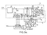
- the phase 3 locked loop can have at least one signal shaping circuit 31 of reference frequency CLK, this circuit 31 being intended to the shaping of this signal and, where appropriate, constituted by a divider by two in order to deliver a signal of 1/2 duty cycle.
- the phase lock loop also includes a three phase / frequency comparator states, marked 32, receiving on a first input the CLK reference frequency signal or the signal shaped by the aforementioned circuit 31 at test point A of Figure 2a. It receives on a second V2 input the signal of reference frequency or the signal shaped by the circuit 31, delivered via the delay circuit auxiliary, i.e. the reference frequency signal subject to the delay of the 2N inverters constituting the auxiliary delay 30.
- the phase / frequency comparator 32 delivers a zero value comparison signal in the absence phase / frequency offset between the signals of the first and second input above and a signal positive or negative value proportional to the offset phase / frequency between the signals of the first and the second entry.
- the resulting signal delivered by the two intensity generators 321 and 322 constitutes the output signal of the phase / frequency comparator in three states 32.
- the above output signal is delivered to a low-pass filter 33, which has the essential function to integrate this output signal in order to deliver the signal phase control V0 previously mentioned.
- the control signal of phase V0 has a determined value corresponding to the integrated value of the output signal delivered by the comparator three-state phase / frequency and the delay provided by the auxiliary delay circuit 30 is equal to the period of the CLK reference frequency signal or at the very least signal delivered by the shaping circuit 31 to point A.
- delay circuit 2 is also slaved to a calibrated value corresponding to the M elementary delays Tp provided by each of the constituent inverters of the delay circuit 2 above.
- the comparator three-state phase / frequency and in particular the comparator itself 320 can be achieved either by through a comparator in CMOS technology, this type of comparator being active in the low state i.e. on the falling edge of transitions, either through a bipolar comparator by means of NOR gates, this type of comparator being active in the high state, that is to say on the rising edge of the transitions.
- connection between point A in Figure 2a and the first input V1 of the three phase / frequency comparator states 32 can be formed by a direct link and the number of cascaded inverters to achieve the auxiliary delay circuit 30 may be an odd number.
- the link between point A, the exit point of the shaping circuit 31 delivering the signals of 1/2 duty cycle reference frequency at input V1 of the three-state phase / frequency comparator must be performed via an inverter and a delay must be brought to the circuit entrance auxiliary delay 30.
- FIG. 3a corresponds to an embodiment in which the locking loop phase 3 is completed by an initialization circuit 4 of the three-state phase / frequency comparator 32 and the delay initial global provided by the auxiliary delay circuit 30 at its minimum value, i.e. at a value initialization corresponding to the control voltage of lowest phase V0 in Figure 2b.
- This operating mode allows an increase in the value of the delay overall provided by the auxiliary delay circuit 30 up to an equilibrium value corresponding to the period of reference frequency signal, as well as previously mentionned.
- the phase / frequency comparator initialization circuit in three states 32 advantageously includes controlled switch circuits KA, KB, KC, KD, these controlled switch circuits being placed between the input V1 of phase / frequency comparator 32, input V2 of phase / frequency comparator 32, the control output of the current generator 321 and the control output of the intensity generator 322 respectively.
- the circuits switches KA, KB, KC, KD allow the switching of actual phase comparator inputs 320, respectively outputs from it, to a logic value 1, corresponding for example to the supply voltage VCC of the device, respectively to the value of the inputs V1, V2, respectively of the corresponding outputs U, D of the comparator phase / frequency proper 320 to control the current generators 321, 322.
- the low-pass filter 33 can be formed by an integration capacity, denoted 330, which is connected to the output of the phase / frequency comparator three states 32 on the one hand, and, on the other hand, at the supply voltage VCC via a controlled switch KE, the integration capacity 330 being on the other hand connected at the reference voltage.
- the limit of integration capacity 330 connected to the KE controlled switch and to the output of the phase / frequency comparator 32, delivers the voltage of phase control V0 to the auxiliary delay circuit 30 and delay circuit 2.
- an initialization circuit proper 4 which includes an ET 40 type logic gate, one of which first input is connected to the input terminal V1 of the phase / frequency comparator 32, upstream of the switch ordered KA and a second input of which is connected to a synchronization control signal S.
- the output of the AND logic gate 40 is connected to a flip-flop 41 whose input D receives synchronization signal S.
- output Q of the flip-flop 41 is connected to a controlled switch 43, itself connected to the reference voltage, this switch controlled 43 being controlled, via an inverter 42, via the synchronization signal S.
- the Q output of flip-flop 41 delivers a control signal of all controlled switches KA, KB, KC, KD, KE.
- the initialization circuit as described in relation with FIG. 3a operates in the following manner.
- the complemented signal AT delivered by the inverter 310 is applied to the control input or clock of the flip-flop 41 and the output Q of the latter is then controlled at state 1, the control signal from the switches KA, KB, KC and KD thus being released.
- Flip-flop 41 changes to state 1 at the first rising edge of the signal AT above and thus causes the switching of the controlled switches KA, KB, KC, KD, KE.
- the signal AT delivered by the inverter 310 and the signal B delivered by the auxiliary delay circuit 30 are necessarily in the high state and the first falling edge which occurs is a falling edge of B, which is applied to the input V2 and by via the controlled switch KB, to the phase / frequency comparator proper 320.
- the comparator then makes it possible to carry out the comparison in the direction of increasing the delay and therefore decreasing the phase control voltage V0 .
- FIG. 3b The various aforementioned parameters are represented in FIG. 3b in which the signal A delivered at the output of the shaping circuit 31 is successively represented, the signal AT supplemented by the latter, delivered by the inverter 310, the signal B delivered by the auxiliary delay circuit 30 and the signal D delivered at the output D of the phase / frequency comparator proper 320, that is to say when the controlled switch KD is closed, on command of the intensity generator 322.
- this detector can be varied without however departing from the scope of the subject of the present invention. It is indicated that it is possible to use a sensitive phase / frequency comparator on a rising edge or descending signals, non-reversing gates to the place of reversers as well as rockers constituting either the divider by two of the shaping circuit 31, i.e. the flip-flop 41, sensitive on rising or falling edge.
- the number M of cascaded inverters to achieve the delay circuit 2 can be even or odd and finally, the exclusive OR gate 1 can be replaced by a circuit equivalent NOR type in corresponding complemented logic.
- the shaping circuit normally constituted by a bistable rocker 31 can be eliminated.
- the time of propagation Tp of the inverters can be carried out either in voltage, via the control voltage of phase V0, also in current.
- phase / frequency comparator itself 320 can be made either on the basis of logic circuits of the type NON-OR, either of the NAND type.
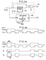
- phase comparator such as previously mentioned, at the VD detector, transition as described previously in the description, is associated in parallel on the represented data flow by the logic signal an auxiliary channel VA formed by a flip-flop, noted 50, and an OR gate of the type exclusive, noted 51.
- the flip-flop 50 receives a signal clock associated with the logic input signal, represented by "Data", this signal also being delivered on an input of the exclusive OR type door 51.
- the output of the scale bistable delivers a logic signal synchronized with the signal clock, noted CLO, this signal being delivered to the input of the flip-flop 50.
- the pulses generated by the detector VD and corresponding to the signal noted Sp have a constant duration equal to the Tp value (see Fig. 2c).
- the pulses generated by the auxiliary channel VA and corresponding to signal S1 have a variable duration, which is a measurement of the phase shift of the "Data" logic signal by with respect to the CLO clock signal. Because of the same peak-to-peak amplitude in value and sign, i.e. for the same transition direction of the two pulses delivered by the VD detection channel and the VA auxiliary channel, a differential measure of the average value of the two S1 and Sp signals can be performed with peak ripple of the minimum differential signal when the phase balance is reached.
- the device as shown in Figure 4a allows for a phase comparator similarly type that the HOGGE comparator previously described, but with the advantage of being able to cancel the 180 ° phase shift between the two comparison pulses delivered by the VD detection channel and VA auxiliary channel.
- phase comparator device as described in figure 4a can be used in a phase-locked loop (PLL) for extracting the CLO serial clock of the corresponding digital data signal "Data”, and that it can also be used to different types of digital data encoding format.
- PLL phase-locked loop
- the data signal For a digital data signal or logic signal of NRZ type previously cited and designated by "Data" and its associated clock signal CLO, the data signal has a bit period designated by T bit .
- the value of the parameter P which is an integer depends on the type of decoder-encoder used.
- the detection channel VD corresponding to the transition detector circuits as shown in FIG. 2a or 3a receives for clock signal CLK the above-mentioned reference frequency signal F MOT .
- phase diagram An example of a phase diagram is given on the Figure 4c for which at equilibrium the phase difference ⁇ between the signals S1 delivered by the auxiliary channel VA and Sp delivered by the VD detection channel is given in FIG. 4c.
- pulses S1 and Sp are in phase at equilibrium, which, for a differential detection of average value on signals S1 and Sp, allows to measure phase shift with comparatively reduced peak ripple to the HOGGE device.
- the remarkable property self-centering of a CLO clock rising edge in the middle of bit of digital signal "Data" is also maintained.
- the static phase excursion of the comparator phase thus carried out remains equal to ⁇ 180 °.
- the bit frequency, F bit being generally related to the word frequency, F MOT , by an integer and constant division ratio P, it is easily understood that a modification of F bit also causes a proportional modification of F MOT .
- the operation of the phase comparator described above is independent of the bit frequency, F bit , as long as the value of P does not change and that the pulse duration of the signal Sp remains compatible with a normal operation of the VD detection channel.
Landscapes
- Physics & Mathematics (AREA)
- Nonlinear Science (AREA)
- Engineering & Computer Science (AREA)
- Computer Networks & Wireless Communication (AREA)
- Signal Processing (AREA)
- Stabilization Of Oscillater, Synchronisation, Frequency Synthesizers (AREA)
Claims (6)
- Detektor für den Übergang eines logischen Signals, der ein logisches Exklusiv-Oder-Gatter aufweist, dessen erster Eingang das logische Signal empfängt und dessen zweiter Eingang das logische Signal über einen Verzögerungskreis von einer bestimmten Verzögerung empfängt, wobei dieser Dektektor außerdem einen Zusatzverzögerungskreis aufweist, der dem Verzögerungskreis über eine Phasenverriegelungsschleife zugeordnet ist, wobei diese Phasenverriegelungsschleife es gestattet, ausgehend von einem Bezugsfrequenzsignal, das an den Eingang des Zusatzverzögerungskreises angelegt ist, ein gemeinsames Phasensteuersignal zu erzeugen, das die Regelung der von dem Verzögerungskreis und dem Zusatzverzögerungskreis eingeführten Verzögerung auf einen zur Periode des Bezugsfrequenzsignals proportionalen Wert gestattet, was bei jedem Übergang des logischen Signals die Erzeugung eines kalibrierten Impulses gestattet, dessen Dauer zu der Periode des Bezugsfrequenzsignals proportional ist.
- Detektor nach Anspruch 1, dadurch gekennzeichnet, dass der Verzögerungskreis von einer Vielzahl von M kaskadenförmig geschalteten Umkehrkreisen mit gesteuerter Fortpflanzungszeit gebildet ist und dass der Zusatzverzögerungskreis von einer Vielzahl von 2N kaskadenförmig geschalteten Umkehrkreisen mit gesteuerter Fortpflanzungszeit gebildet ist, wobei diese Umkehrkreise durch das von der Phasenverriegelungsschleife gelieferte Phasensteuersignal gesteuert werden.
- Detektor nach Anspruch 2, dadurch gekennzeichnet, dass die den Verzögerungskreis bzw. den Zusatzverzögerungskreis bildenden Umkehrkreise identisch sind, wobei die durch diesen Verzögerungskreis erzeugte Verzögerung τ gleich dem Produkt aus dem Verhältnis der Anzahl M von den Verzögerungskreis bildenden Umkehrkreisen zur Anzahl 2N von den Zusatzverzögerungskreis bildenden Umkehrkreisen und der Periode Tref des Bezugsfrequenzsignals
- Detektor nach einem der Ansprüche 1 bis 3, dadurch gekennzeichnet, dass die Phasenverriegelungsschleife mindestens folgendes aufweist:einen Phasen/Frequenz-Vergleicher mit drei Zuständen, der auf dem ersten Eingang das Bezugsfrequenzsignal und auf dem zweiten Eingang das über den Zusatzverzögerungskreis gelieferte Bezugsfrequenzsignal empfängt, wobei der Phasen/Fre-quenz-Vergleicher ein Vergleichssignal vom Wert null bei Fehlen einer Phasen/Frequenz-Verschiebung zwischen den Signalen des ersten und des zweiten Eingangs und ein zur Phasen/Frequenz-Verschiebung zwischen den Signalen des ersten und des zweiten Eingangs proportionales Signal mit positivem oder negativem Wert liefert,ein Tiefpassfilter, das dieses Vergleichssignal empfängt und das gemeinsame Phasensteuersignal liefert, das dem Verzögerungskreis und dem Zusatzverzögerungskreis geliefert wird.
- Detektor nach Anspruch 4, dadurch gekennzeichnet, dass der Phasenverriegelungskreis außerdem Mittel zur Initialisierung des Phasen/Frequenz-Vergleichers mit drei Zuständen und der durch den Zusatzverzögerungskreis eingeführten Anfangsgesamtverzögerung auf ihrem Minimumwert aufweist, so dass eine Erhöhung des Werts der durch diesen Zusatzverzögerungskreis eingeführten Gesamtverzögerung bis zu einem Gleichgewichtswert zugelassen wird, der der Periode des Bezugssignals entspricht.
- Verwendung eines Detektors für den Übergang eines logischen Signals nach einem der vorhergehenden Ansprüche zur Bildung eines Phasenvergleichers, bei der dem Detektor parallel zu dem Fluss der von dem logischen Signal dargestellten Daten ein Zusatzkanal zugeordnet ist, der von einem bistabilen Kippkreis, der ein dem logischen Signal zugeordnetes Taktsignal empfängt, und einem Exklusiv-Oder-Gatter gebildet wird, wobei ein Eingang des Exklusiv-Oder-Gatters und der Dateneingang des Kippkreises das logische Signal empfangen und der Ausgang des bistabilen Kippkreises ein auf dieses Taktsignal synchronisiertes logisches Signal liefert, wobei dieser Detektor und dieser Zusatzkanal jeweils einen Phasenvergleichsimpuls derselben Spitze-Spitze-Amplitude liefern, bei dem die Differenz zwischen der Dauer jedes der Impulse ein Maß für die Phasenverschiebung des logischen Signals bezüglich des Taktsignals bei Fehlen von Spitzenwellung im Gleichgewichtszustand bei Differenzerfassung ist.
Applications Claiming Priority (2)
| Application Number | Priority Date | Filing Date | Title |
|---|---|---|---|
| FR9410117 | 1994-08-18 | ||
| FR9410117A FR2723805B1 (fr) | 1994-08-18 | 1994-08-18 | Detecteur de transition d'un signal logique engendrant une impulsion de duree calibree. |
Publications (2)
| Publication Number | Publication Date |
|---|---|
| EP0697768A1 EP0697768A1 (de) | 1996-02-21 |
| EP0697768B1 true EP0697768B1 (de) | 2002-01-23 |
Family
ID=9466371
Family Applications (1)
| Application Number | Title | Priority Date | Filing Date |
|---|---|---|---|
| EP95401893A Expired - Lifetime EP0697768B1 (de) | 1994-08-18 | 1995-08-16 | Eine kalibrierte Impulsbreite erzeugender Detektor für den Übergang eines Logiksignals |
Country Status (3)
| Country | Link |
|---|---|
| EP (1) | EP0697768B1 (de) |
| DE (1) | DE69525114T2 (de) |
| FR (1) | FR2723805B1 (de) |
Families Citing this family (1)
| Publication number | Priority date | Publication date | Assignee | Title |
|---|---|---|---|---|
| US6111812A (en) * | 1999-07-23 | 2000-08-29 | Micron Technology, Inc. | Method and apparatus for adjusting control signal timing in a memory device |
Family Cites Families (8)
| Publication number | Priority date | Publication date | Assignee | Title |
|---|---|---|---|---|
| US4513427A (en) * | 1982-08-30 | 1985-04-23 | Xerox Corporation | Data and clock recovery system for data communication controller |
| US4535459A (en) * | 1983-05-26 | 1985-08-13 | Rockwell International Corporation | Signal detection apparatus |
| JPS62159006U (de) * | 1986-03-31 | 1987-10-08 | ||
| JPS6369315A (ja) * | 1986-09-11 | 1988-03-29 | Sony Corp | Cmos回路を用いた可変遅延装置 |
| JPH02100514A (ja) * | 1988-10-07 | 1990-04-12 | Ricoh Co Ltd | ディレイライン |
| GB2230165B (en) * | 1989-03-30 | 1993-09-15 | Plessey Co Plc | High speed asynchronous data interface |
| US5146121A (en) * | 1991-10-24 | 1992-09-08 | Northern Telecom Limited | Signal delay apparatus employing a phase locked loop |
| US5374894A (en) * | 1992-08-19 | 1994-12-20 | Hyundai Electronics America | Transition detection circuit |
-
1994
- 1994-08-18 FR FR9410117A patent/FR2723805B1/fr not_active Expired - Fee Related
-
1995
- 1995-08-16 DE DE69525114T patent/DE69525114T2/de not_active Expired - Lifetime
- 1995-08-16 EP EP95401893A patent/EP0697768B1/de not_active Expired - Lifetime
Also Published As
| Publication number | Publication date |
|---|---|
| DE69525114D1 (de) | 2002-03-14 |
| FR2723805A1 (fr) | 1996-02-23 |
| DE69525114T2 (de) | 2002-08-29 |
| FR2723805B1 (fr) | 1996-10-25 |
| EP0697768A1 (de) | 1996-02-21 |
Similar Documents
| Publication | Publication Date | Title |
|---|---|---|
| EP0716501B1 (de) | Phasenvergleicher für ein digitales Signal und ein Taktsignal, und entsprechender Phasenregelkreis | |
| WO2008142268A2 (fr) | Dispositif d'extraction d'horloge a asservissement numérique de phase sans réglage externe | |
| EP0015014B1 (de) | Vorrichtung zur schnellen Synchronisierung eines Taktsignals | |
| EP0500473A1 (de) | Phasen/Frequenzkomparator für Taktrückgewinnungssystem | |
| FR2787651A1 (fr) | Detecteur numerique de frequence de phase | |
| EP1424774B1 (de) | Zufallszahlengenerator | |
| EP0147307B1 (de) | Frequenzsynthesierer mit gebrochenem Teilungsverhältnis und mit schwachem Phasenrauschen und Anwendung dieser Synthesierer | |
| EP0190730A1 (de) | Einrichtung zur Dreifachtaktverteilung, wobei jedes Taktsignal ein Synchronisationssignal enthält | |
| EP0881772B1 (de) | Frequenzteilungsvorrichtung, bestehend aus einem Vorzähler gefolgt von einem programmierbaren Zähler und Anwendung in einem Frequenzsynthetisierer | |
| FR2480048A1 (fr) | Boucle analogique a verrouillage en frequence | |
| FR2478398A1 (fr) | Controle numerique de la vitesse d'un moteur | |
| BE897171A (fr) | Dispositif d'asservissement en frequence d'une horloge sur un signal exterieur de frequence moyenne tres precise mais comportant une gigue importante, | |
| EP0134374B1 (de) | Phasenverriegelter Taktgeber | |
| FR2773925A1 (fr) | Synthetiseur de frequence a boucle d'asservissement en phase avec circuit de detection d'asservissement | |
| EP0302562B1 (de) | Frequenz-Synthetisierer mit einer Abstimm-Anzeigeeinrichtung | |
| EP0715415A1 (de) | Vorrichtung zur Parallelserienwandlung von binären Daten mit hoher Datenrate | |
| EP0064923B1 (de) | System zur Phasensynchronisation digitaler Datenströme und seine Verwendung bei der Umschaltung der Datenströme | |
| EP0697768A1 (de) | Eine kalibrierte Impulsbreite erzeugender Detektor für den Übergang eines Logiksignals | |
| EP0289385B1 (de) | Referenzzeitvorrichtung mit konstanter Stabilität für Kurz- und Langzeitmessungen | |
| EP0526359B1 (de) | Verfahren und Schaltungsanordnung zur Synchronisierung eines Signals | |
| EP0246135B1 (de) | Phasen- und Frequenzdetektor und seine Anwendung in einer Phasenregelschleife | |
| EP0689315B1 (de) | Phasenkomparator | |
| FR2770704A1 (fr) | Circuit verrouille en phase | |
| EP0244316B1 (de) | CMI-Dekodierer | |
| EP2143231B1 (de) | Vorrichtung zur rückgewinnung des taktes und digitaler daten ohne extenre regelung |
Legal Events
| Date | Code | Title | Description |
|---|---|---|---|
| PUAI | Public reference made under article 153(3) epc to a published international application that has entered the european phase |
Free format text: ORIGINAL CODE: 0009012 |
|
| AK | Designated contracting states |
Kind code of ref document: A1 Designated state(s): DE GB IT NL |
|
| 17P | Request for examination filed |
Effective date: 19960112 |
|
| RAP1 | Party data changed (applicant data changed or rights of an application transferred) |
Owner name: MHS |
|
| 17Q | First examination report despatched |
Effective date: 19980721 |
|
| GRAG | Despatch of communication of intention to grant |
Free format text: ORIGINAL CODE: EPIDOS AGRA |
|
| GRAG | Despatch of communication of intention to grant |
Free format text: ORIGINAL CODE: EPIDOS AGRA |
|
| GRAH | Despatch of communication of intention to grant a patent |
Free format text: ORIGINAL CODE: EPIDOS IGRA |
|
| RAP1 | Party data changed (applicant data changed or rights of an application transferred) |
Owner name: ATMEL NANTES SA |
|
| GRAH | Despatch of communication of intention to grant a patent |
Free format text: ORIGINAL CODE: EPIDOS IGRA |
|
| GRAH | Despatch of communication of intention to grant a patent |
Free format text: ORIGINAL CODE: EPIDOS IGRA |
|
| GRAA | (expected) grant |
Free format text: ORIGINAL CODE: 0009210 |
|
| REG | Reference to a national code |
Ref country code: GB Ref legal event code: IF02 |
|
| AK | Designated contracting states |
Kind code of ref document: B1 Designated state(s): DE GB IT NL |
|
| REF | Corresponds to: |
Ref document number: 69525114 Country of ref document: DE Date of ref document: 20020314 |
|
| GBT | Gb: translation of ep patent filed (gb section 77(6)(a)/1977) |
Effective date: 20020425 |
|
| PLBE | No opposition filed within time limit |
Free format text: ORIGINAL CODE: 0009261 |
|
| STAA | Information on the status of an ep patent application or granted ep patent |
Free format text: STATUS: NO OPPOSITION FILED WITHIN TIME LIMIT |
|
| 26N | No opposition filed | ||
| PGFP | Annual fee paid to national office [announced via postgrant information from national office to epo] |
Ref country code: NL Payment date: 20090722 Year of fee payment: 15 Ref country code: GB Payment date: 20090807 Year of fee payment: 15 |
|
| PGFP | Annual fee paid to national office [announced via postgrant information from national office to epo] |
Ref country code: IT Payment date: 20090820 Year of fee payment: 15 |
|
| PGFP | Annual fee paid to national office [announced via postgrant information from national office to epo] |
Ref country code: DE Payment date: 20100827 Year of fee payment: 16 |
|
| REG | Reference to a national code |
Ref country code: NL Ref legal event code: V1 Effective date: 20110301 |
|
| GBPC | Gb: european patent ceased through non-payment of renewal fee |
Effective date: 20100816 |
|
| PG25 | Lapsed in a contracting state [announced via postgrant information from national office to epo] |
Ref country code: NL Free format text: LAPSE BECAUSE OF NON-PAYMENT OF DUE FEES Effective date: 20110301 Ref country code: IT Free format text: LAPSE BECAUSE OF NON-PAYMENT OF DUE FEES Effective date: 20100816 |
|
| PG25 | Lapsed in a contracting state [announced via postgrant information from national office to epo] |
Ref country code: GB Free format text: LAPSE BECAUSE OF NON-PAYMENT OF DUE FEES Effective date: 20100816 |
|
| REG | Reference to a national code |
Ref country code: DE Ref legal event code: R119 Ref document number: 69525114 Country of ref document: DE Effective date: 20120301 |
|
| PG25 | Lapsed in a contracting state [announced via postgrant information from national office to epo] |
Ref country code: DE Free format text: LAPSE BECAUSE OF NON-PAYMENT OF DUE FEES Effective date: 20120301 |