EP0700081A2 - Procédé pour former un dispositif semi-conducteur de circuits intégrés comportant des contacts en silicide auto-alignés sur les régions - Google Patents
Procédé pour former un dispositif semi-conducteur de circuits intégrés comportant des contacts en silicide auto-alignés sur les régions Download PDFInfo
- Publication number
- EP0700081A2 EP0700081A2 EP95113564A EP95113564A EP0700081A2 EP 0700081 A2 EP0700081 A2 EP 0700081A2 EP 95113564 A EP95113564 A EP 95113564A EP 95113564 A EP95113564 A EP 95113564A EP 0700081 A2 EP0700081 A2 EP 0700081A2
- Authority
- EP
- European Patent Office
- Prior art keywords
- region
- forming
- regions
- layer
- source
- Prior art date
- Legal status (The legal status is an assumption and is not a legal conclusion. Google has not performed a legal analysis and makes no representation as to the accuracy of the status listed.)
- Withdrawn
Links
Images


Classifications
-
- H—ELECTRICITY
- H10—SEMICONDUCTOR DEVICES; ELECTRIC SOLID-STATE DEVICES NOT OTHERWISE PROVIDED FOR
- H10D—INORGANIC ELECTRIC SEMICONDUCTOR DEVICES
- H10D30/00—Field-effect transistors [FET]
- H10D30/01—Manufacture or treatment
- H10D30/021—Manufacture or treatment of FETs having insulated gates [IGFET]
- H10D30/0223—Manufacture or treatment of FETs having insulated gates [IGFET] having source and drain regions or source and drain extensions self-aligned to sides of the gate
-
- H—ELECTRICITY
- H10—SEMICONDUCTOR DEVICES; ELECTRIC SOLID-STATE DEVICES NOT OTHERWISE PROVIDED FOR
- H10P—GENERIC PROCESSES OR APPARATUS FOR THE MANUFACTURE OR TREATMENT OF DEVICES COVERED BY CLASS H10
- H10P14/00—Formation of materials, e.g. in the shape of layers or pillars
- H10P14/40—Formation of materials, e.g. in the shape of layers or pillars of conductive or resistive materials
-
- H—ELECTRICITY
- H10—SEMICONDUCTOR DEVICES; ELECTRIC SOLID-STATE DEVICES NOT OTHERWISE PROVIDED FOR
- H10D—INORGANIC ELECTRIC SEMICONDUCTOR DEVICES
- H10D30/00—Field-effect transistors [FET]
- H10D30/01—Manufacture or treatment
- H10D30/021—Manufacture or treatment of FETs having insulated gates [IGFET]
- H10D30/0212—Manufacture or treatment of FETs having insulated gates [IGFET] using self-aligned silicidation
-
- H—ELECTRICITY
- H10—SEMICONDUCTOR DEVICES; ELECTRIC SOLID-STATE DEVICES NOT OTHERWISE PROVIDED FOR
- H10D—INORGANIC ELECTRIC SEMICONDUCTOR DEVICES
- H10D64/00—Electrodes of devices having potential barriers
- H10D64/20—Electrodes characterised by their shapes, relative sizes or dispositions
- H10D64/23—Electrodes carrying the current to be rectified, amplified, oscillated or switched, e.g. sources, drains, anodes or cathodes
- H10D64/251—Source or drain electrodes for field-effect devices
- H10D64/258—Source or drain electrodes for field-effect devices characterised by the relative positions of the source or drain electrodes with respect to the gate electrode
- H10D64/259—Source or drain electrodes being self-aligned with the gate electrode and having bottom surfaces higher than the interface between the channel and the gate dielectric
-
- H—ELECTRICITY
- H10—SEMICONDUCTOR DEVICES; ELECTRIC SOLID-STATE DEVICES NOT OTHERWISE PROVIDED FOR
- H10W—GENERIC PACKAGES, INTERCONNECTIONS, CONNECTORS OR OTHER CONSTRUCTIONAL DETAILS OF DEVICES COVERED BY CLASS H10
- H10W20/00—Interconnections in chips, wafers or substrates
- H10W20/01—Manufacture or treatment
- H10W20/031—Manufacture or treatment of conductive parts of the interconnections
- H10W20/0698—Local interconnections
-
- H—ELECTRICITY
- H10—SEMICONDUCTOR DEVICES; ELECTRIC SOLID-STATE DEVICES NOT OTHERWISE PROVIDED FOR
- H10D—INORGANIC ELECTRIC SEMICONDUCTOR DEVICES
- H10D64/00—Electrodes of devices having potential barriers
- H10D64/01—Manufacture or treatment
- H10D64/017—Manufacture or treatment using dummy gates in processes wherein at least parts of the final gates are self-aligned to the dummy gates, i.e. replacement gate processes
Definitions
- the instant invention relates to microelectronic technology and semiconductor processing, and, more specifically, to a method of fabricating a semiconductor device with self-aligned silicide regions for integrated circuits.
- CMOS complementary metal-oxide-semiconductor
- SRAM static random access memory
- CMOS complementary metal-oxide-semiconductor
- silicide self-aligned silicide regions
- semiconductor technologies scale to the sub-half-micron minimum feature size regime, junction leakage requirements place a serious constraint on the maximum initial refractory metal (for example, titanium or cobalt) thickness. This is due to the requirement that the amount of silicon consumption over the source/drain junction regions must be reduced in order to prevent junction leakage problems. This will, however, increase the silicide sheet resistance and reduce the benefit of the salicide formation due to increased parasitic source/drain and gate resistance elements.
- IGFET insulated-gate field-effect transitor
- This method is based on the combination of self-aligned silicide and selective chemical-vapor deposited tungsten ("CVD-W”) processes.
- This method employs a relatively thin layer of initial refractory metal layer (for example the titanium layer would be less than 500 ⁇ thick) to form a salicide structure without excessive silicon consumption.
- the salicide process is then followed by selective chemical-vapor deposition of tungsten ("CVD-W”) to further reduce the source/drain junction and gate sheet resistance values due to the CVD-W/TiSi2 stack structure over these regions.
- CVD-W selective chemical-vapor deposition of tungsten
- the CVD-W to TiSi2 contact resistance can become rather high due to the action of fluorine during the CVD-W process, which can result in the formation of a nonvolatile insulating TiF x compound at the CVD-W/TiSi2 interface.
- Selective CVD-W processes usually employ a process medium consisting of WF6, SiH4, and H2. Tungsten is selectively deposited (typically at a substrate termperature of 300°C) on the regions with exposed silicon and/or metallic coating. The TiF x formation process may occur due to presence of fluorine caused by WF6.
- this method may introduce the formation of wormholes in silicon due to CVD-W, which can result in excessive junction leakage.
- This invention provides a fully self-aligned processing technique for fabrication of sub-half-micron salicided devices (including IGFETs) with very small, on the order of less than 300 ⁇ , silicon consumption and very low source/drain junction and gate sheet resistance values.
- An embodiment of the present invention is a method which does not require any selective deposition processes and employs standard silicon processing resources.
- the method of the present invention also provides a silicide local interconnect as a byproduct of the fabrication process flow.
- a method for fabricating a semiconductor device with a self-aligned silicide region comprising forming insulating regions on a substrate, forming a gate region insulatively disposed over said substrate and situated between said insulating regions, forming source/drain regions with a channel region therebetween source/drain regions being formed in said substrate adjacent to said gate region and extending from said gate region to said insulating regions, forming a self-aligned silicide region on said source/drain regions, forming a plurality of electrically conductive regions, each electrically conductive region contacting one of said source/drain regions, and simultaneously forming another electrically conductive region on the gate region.
- a semiconductor device having a self-aligned silicide region comprising a plurality of insulating region overlying a substrate, a gate region insulatively disposed over said substrate and situated between said insulating regions, source/drain regions with a channel region therebetween, said source/drain regions being formed in said substrate adjacent to said gate region and extending from said gate region to said insulating regions, a self-aligned silicide region formed on said source/drain regions, and a plurality of electrically conductive regions, each region contacting one of said source/drain regions, and another electrically conductive region formed on the gate region.
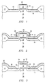
- Figures 1-5 are cross sectional views of two embodiments of the present invention.
- Figures 1-3 illustrate the fabrication of one embodiment of the present invention.
- Figures 4 and 5 illustrate another embodiment.
- Figure 6 is a cross sectional view of of a CMOS device structure which can utilize the embodiments of this invention.
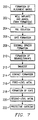
- Figure 7 illustrates a CMOS process flow which can incorporate an embodiment of the present invention for salicide formation.
- the process flow of the present invention is shown with respect to an NMOS device.
- PMOS devices can be simultaneously fabricated using the process flow of the instant invention.
- the process flow illustrated by the devices of Figures 1-5 is for non-LDD (i.e. a device not having lightly doped source/drain junction regions) devices.
- Devices having LDD's can also be fabricated using the process flow of the instant invention for the salicide process.
- the process flows of this invention can also be used for fabricaion of self-aligned bipolar junction transistor.
- a semiconductor layer (preferably a doped epitaxial silicon layer) may be deposited on the semiconductor wafer resulting in a substrate with a lightly doped epitaxial layer on a heavily doped region.
- the semiconductor wafer/semiconductor layer is illustrated as region 26 and will generically be called "semiconductor layer 26" throughout the specification.
- Semiconductor layer 26 may either be in situ doped at deposition, subsequently doped or any other standard method of doping a semiconductor wafer or semiconductor layer.
- semiconductor layer 26 is doped with a p-type dopant, such as in a CMOS p-well region.
- CMOS well regions 15 are formed, next, using the alignment marks for exact positioning of the n-well and p-well regions.
- well regions 15 are doped with a p-type dopant, such as boron, in order to create what is commonly referred to as p-well regions.
- field oxide regions 12 are formed using a process such as local oxidation of silicon (LOCOS).
- LOCOS local oxidation of silicon
- Field oxide regions 12 are aligned with respect to the microlithography alignment marks. After field oxides 12 are formed, a thin layer of insulating material, preferably silicon dioxide, is formed by a process such as thermal oxidation. Next a layer of conducting material is deposited, preferably polysilicon, over the insulating layer to be used as the CMOS gate electrode. The conducting layer is then patterned and etched so as to form transistor gate region 10 over gate dielectric layer 24. Next, side wall spacer regions 18 are formed by depositing a conformal layer of dielectric material and anisotropically etching that material using an anisotropic reactive ion etch process.
- insulating material preferably silicon dioxide
- conducting material is deposited, preferably polysilicon, over the insulating layer to be used as the CMOS gate electrode.
- the conducting layer is then patterned and etched so as to form transistor gate region 10 over gate dielectric layer 24.
- side wall spacer regions 18 are formed by depositing a conformal layer of dielectric material and aniso
- Heavily doped source/drain junction regions 14 are formed by an ion implantation process followed by a thermal anneal process. This results in the formation of n+ source/drain junctions for NMOS transistors. A separate ion implantation step is used to form the p+ source/drain junctions for PMOS transistors.
- the next process step is to deposit a thin layer (preferably on the order of 200 ⁇ thick) of refractory metal (preferably titanium) using a suitable deposition process such as physical-vapor deposition (PVD).
- a silicide react process is preformed.
- a titanium silicide react process may be performed in a rapid thermal processing (RTP) reactor in a nitrogen ambient at 650 to 700°C.
- RTP rapid thermal processing
- metal nitride such as titanium nitride
- the only remaining refractory metal material regions on the transistor source/drain junction and gate regions are refractory metal silicide regions 16 and 20, respectively.
- layer 27 (preferably WSi x ) is deposited (preferably by a low temperature, less then 400°C, SiH4/H2/WF6 based CVD process).
- layer 27 preferably WSi x
- WSi x a low temperature, less then 400°C, SiH4/H2/WF6 based CVD process.
- commercially available equipment will be used to deposit the WSi x layer with an X value in the range of 2.0 to 2.7. This can be accomplished by using a process which deposits a bilayer of WSi x , where the X-value is near the stoichiometric value of 2 for most of the layer and between the values of 2.4 and 2.7 for a thin portion (on the order of 50-100 ⁇ ) of the layer near the top.
- the total WSi x layer thickness may be on the order of 500 to 1500 ⁇ .
- the graded stoichiometry is a preference and not a requirement. It can be easily handled by commercial CVD-WSi x equipment.
- the CVD-WSi x deposition process parameters may be selected to promote a nonconformal deposition process (i.e. thinner WSi x layer on the sidewalls).
- a thin (preferably on the order of 100 to 300 ⁇ ) conformal layer of insulating material preferably a silicon nitride oxidation mask layer
- LPCVD low-pressure chemical-vapor deposition
- the LPCVD silicon nitride process temperature preferably around 800°-850°C
- the LPCVD silicon nitride process temperature also acts as an anneal process for resistivity reduction of both the refractory metal salicide (preferably TiSi2) regions 16 and 20 and conductive layer 27 (preferably CVD-WSi x ).
- a short anisotropic silicon nitride etch is performed using layer 27 as an etch stop layer.
- This anisotropic nitride etch process may be performed in a high-density plasma source such as an inductively coupled plasma (ICP) reactor.
- ICP inductively coupled plasma
- thin insulating filament spacers 28 which mask the portions of layer 27 which are alongside gate sidewall spacers 18.
- thin insulating filament spacers 28 are formed of silicon nitride due to its excellent oxidation mask characteristics.
- a short low-temperature (preferably on the order of 750°C to 850°C) thermal oxidation is performed so as to grow a thin (approximately 50 to 100 ⁇ ) SiO2 layer over exposed regions of layer 27.
- the portion of layer 27 over the gate sidewall is not oxidized due to the oxidation masking effect of thin silicon nitride spacers 28.
- thin silicon nitride spacers 28 are stripped using a selective isotropic etch (plasma or wet) which etches only thin silicon nitride spacers 28 and nothing else.
- a timed selective etch (such as an isotropic SF6 plasma etch) is performed to remove the portion of layer 27 (preferably a CVD WSi x layer) which lies along gate sidewalls spacer regions 18.
- layer 27 preferably a CVD WSi x layer
- the portion of layer 27 over the gate, source/drain and field oxide regions is protected by the thin (preferably on the order of 50 - 100 ⁇ ) grown oxide cap (referred to as 32 and 30, respectively).
- the portion of layer 27 that overlies gate 10 is referred to as region 34 and the portion of layer 27 that overlies source/drain junctions regions 14 and field oxide regions 12 is referred to as region 36.
- any overetch during the removal of the portions of layer 27 that were situated alongside sidewall spacer regions 18 does not etch silicon from source/drain junction regions 14 and gate region 10 since these regions are fully sealed by thin refractory metal silicide layers 16 and 20 (preferably TiSi2), respectively.
- thin refractory metal silicide layers 16 and 20 preferably TiSi2
- the use of a thin Si-rich WSi x (x ⁇ 2.4-2.7) region over layer 27 ensures acceptable SiO2 growth during the short low-temperature CVD-WSi x thermal oxidation process.
- CMOS device structure such as the one depicted in Figure 6.
- a local interconnect mask is utilized to form the CVD-WSi x local interconnects by a lithography and CVD-WSi x etch steps. This is a major advantage over the conventional TiN local interconnect technology.
- the CVD-WSi x local interconnect is a free byproduct of this invention.
- CVD-WSi x local interconnects can be easily patterned by relatively environmentally safe plasma chemistries such as SF6 plasma.
- the subsequent device fabrication process steps are performed so as to form the device contacts and multilevel interconnect structures.
- the CVD-WSi x layer over the source/drain junction and gate regions also serves as an excellent etch-stop layer during the subsequent contact etch process. This prevents any junction silicon overetch or junction damage. This is a very important feature for enhancing manufacturing yield. Therefore, the contact etch process can use excessive (on the order of 50-100%) overetch without causing any junction leakage or device reliability problems due to the effective CVD-WSi x etch stop region over the TiSi2-sealed junctions. Moreover, the CVD-WSi x junction straps may also eliminate the need for collimated Ti sputter deposition after contact etch.
- the process flow of the present invention allows formation of CVD-WSi x steps with thicknesses as large as 1000 to 1500 ⁇ for typical polysilicon gate heights of 3000 to 4000 ⁇ . If the ultimate polysilicon gate thickness is less than 3000 ⁇ (for example, 2500 ⁇ for 0.25-0.35 ⁇ m technologies) and/or if a thicker CVD-WSi x strap is desired over the source/drain junctions and the gate structure (e.g., greater than 1500 ⁇ CVD-WSi x ), then the process flow illustrated in Figures 4 and 5 should be used.
- a conductive layer (not shown), preferably polysilicon, is deposited over the existing structures.
- a disposable layer preferably silicon nitride, is deposited over the conducting layer.
- the conductive layer and the silicon nitride layer are anisotropically etched so as to form conductive gate structure 40 and patterned disposable layer 58, respectively.
- sidewall dielectric spacers 48 and silicide regions 56 are formed, and excess refractory metal and/or metal nitride is removed.
- silicided regions 56 over source/drain junctions 44. Due to the presence of disposable silicon nitride layer 58, no silicide is formed on gate electrode polysilicon region 40. After sidewall spacers 48 and silicide regions 56 are formed, disposable silicon nitride layer 58 is selectively removed, preferably by a plasma etch (or wet etch) process.
- the self-aligned silicide regions can be performed either before or after removal of the disposable silicon nitride layer 58.
- the result of forming the silicided regions before the removal of silicon nitride layer 58 is depicted in Figure 4.
- the result of forming the silicided regions after the removal of silicon nitride layer 58 is depicted in Figure 4a.
- the main difference between these two devices is the presence of silicided region 41 on conductive gate structure 40 and the absence of silicon nitride layer 58 in Figure 4a.
- the device of Figure 4a will look like the device of Figure 5 (with additional processing) except for the presence of silicide region 41 between conductive gate structure 40 and conductive region 62.
- a conductive layer (such as CVD-WSi x ) is deposited, which fills the trench created by the removal of disposable silicon nitride layer 58 to form conductive region 62.
- a thin oxidation mask layer is deposited (preferably silicon nitride).
- the thin oxidation mask layer is anisotropically etched leaving a region of the thin oxidation mask layer which covers the portion of the conductive layer (preferably CVD-WSi x ) that is situated along the sidewall spacer.
- the wafer is subjected to an oxidizing atmosphere which grows a thermal oxide layer on the exposed regions of the conductive layer surface.
- an oxide is formed over the entire CVD-WSi x surface except on the sidewall regions where the CVD-WSi x oxidation is prevented due to the oxidation masking effect of the silicon nitride sidewall spacers.
- a selective etch is subsequently preformed. During this process step only the remaining sidewall silicon nitride spacers are etched and thereby a region of the conducting layer (preferably CVD-WSi x ), along the side wall spacer, is exposed.
- the exposed portion of the conducting layer is subsequently etched, using a selective etch process, and the remaining portions of the conducting layer are shown in Figure 5 as regions 60 and 62.
- Figure 5 illustrates the remaining portions of the oxide layer, which are designated as region 64 and 66.
- the remaining device favrication process flow proceeds using standard integrated circuit fabrication processes in order to form the local interconnect and multilevel interconnect structures.
- Figure 6 illustrates a schematic diagram of CMOS-type devices which can utilize the fabrication process of the present invention. While the devices of Figure 6 refer to specific dopant types, it is possible to fabricate these devices using dopants of the opposite conductivity type while still utilizing the processing steps of the instant invention.
- Substrate 100 is fabricated using p-type dopants (preferably the substrate is heavily doped with boron), and epitaxial layer 102 is also p-type (preferably the epitaxial layer is lightly doped with boron).
- the CMOS p-well regions 104 and n-well regions 106 are formed in boron-doped epitaxial layer 102 using boron and phosphorus ion implantations, respectively, followed by a thermal anneal process.
- Regions 114 and 116 are n+ source/drain junction regions and regions 108 and 112 are p+ source/drain junction regions.
- Field oxide isolation regions 110 are formed between the devices and sidewall spacer regions 128 are formed adjacent NMOS and PMOS transistor gate structures 130 and 131.
- TEOS oxide layer 120 is deposited over both devices, preferably by low-pressure chemical-vapor deposition (LPCVD). Overlying TEOS 120 is TEOS boro-phospho-silicate glass (BPSG) layer 118 which is preferably deposited by plasma-enhanced chemical-vapor deposition (PECVD) and is subsequently reflowed using thermal BPSG reflow techniques.
- PECVD plasma-enhanced chemical-vapor deposition
- second BPSG layer 122 is situated above the first BPSG layer 118 and after formaiton of the first patterned interconnect level.
- Interconnects 134 and 135, which connect source/drain junction regions 108, 112, 114 and 116 as well as CMOS gates 130 and 131 to the other devices, are fabricated using CVD-W or reflowed aluminum. Regions 136, formed underneath interconnects 134 and 135, are Ti/TiN bilayers fabricated using collimated sputtering. Layers of PECVD TEOS oxide (i.e. regions 124 and 138) are formed over BPSG layers 118 and 122. The stacked layer of PECVD TEOS oxide 138 and PECVD silicon nitride layer 140 is formed as a protective overcoat.
- the fabrication process flows of this invention for formation of low-resistance source/drain junctions and CMOS gate electrodes can be easily integrated in any CMOS or BiCMOS technology including the aforementioned devices.
- FIG. 7 is an illustration of a process flow which can be used to fabricate a CMOS device such as the one depicted in Figure 6.
- the process flow of Figure 7 includes the process flow of the present invention (which is included in salicide process module 212).
- the first step in the process flow of Figure 7 is the formation of alignment marks. This first step is illustrated by block 200, and includes a first mask and semiconductor etch.
- Second step 202 is the formation of CMOS well regions. Step 202 includes forming a thin oxide layer on the surface of the semiconductor layer (or substrate), performing masked well implants (boron and phosphorous for p-well and n-well regions, repectively), performing the CMOS well formation thermal anneal, and stripping the thin oxide layer.
- step 204 is preformed to form PBL isolation.
- the poly-buffered LOCOS (PBL) isolation process module consists of forming a patterned stached structure of silicon nitride/polysilicon/silicon dioxide, performing a filed oxidation process, and removing the PBL oxidation mask stack. This results in the formation of patterned field oxide regions.
- Step 206 forms the patterned CMOS gate structure and step 208 forms the sidewall dielectric spacers which are adjacent to the CMOS gate structures.
- source/drain junction regions are formed in step 210.
- Step 210 includes formation of an implant screen oxide, patterned.
- NMOS implants preferably arsenic or phosphorous
- PMOS implants preferably boron
- a rapid thermal anneal step to form the source/drain junction regions.
- salicide process module 212 is performed. Included in step 212 is the deposition of a refractory metal (preferably titanium), a rapid thermal silicide formation process, stripping away the unreacted titanium and titanium nitride, and a rapid thermal anneal of the silicided regions. The process steps of this invention are included in salicide process module 212.
- contacts are formed in step 214. This is followed by the formation of the first-level metal (step 216), the formation of via's (step 218), the formation of the second-level metal (step 220) and the deposition of a protective overcoat (step 222).
Landscapes
- Electrodes Of Semiconductors (AREA)
- Insulated Gate Type Field-Effect Transistor (AREA)
- Metal-Oxide And Bipolar Metal-Oxide Semiconductor Integrated Circuits (AREA)
Applications Claiming Priority (2)
| Application Number | Priority Date | Filing Date | Title |
|---|---|---|---|
| US08/298,018 US6200871B1 (en) | 1994-08-30 | 1994-08-30 | High performance self-aligned silicide process for sub-half-micron semiconductor technologies |
| US298018 | 1994-08-30 |
Publications (2)
| Publication Number | Publication Date |
|---|---|
| EP0700081A2 true EP0700081A2 (fr) | 1996-03-06 |
| EP0700081A3 EP0700081A3 (fr) | 1997-07-02 |
Family
ID=23148649
Family Applications (1)
| Application Number | Title | Priority Date | Filing Date |
|---|---|---|---|
| EP95113564A Withdrawn EP0700081A3 (fr) | 1994-08-30 | 1995-08-29 | Procédé pour former un dispositif semi-conducteur de circuits intégrés comportant des contacts en silicide auto-alignés sur les régions |
Country Status (5)
| Country | Link |
|---|---|
| US (1) | US6200871B1 (fr) |
| EP (1) | EP0700081A3 (fr) |
| JP (1) | JPH08111527A (fr) |
| KR (1) | KR100372675B1 (fr) |
| TW (1) | TW301780B (fr) |
Cited By (2)
| Publication number | Priority date | Publication date | Assignee | Title |
|---|---|---|---|---|
| EP0969516A3 (fr) * | 1998-06-30 | 2004-09-15 | Sharp Kabushiki Kaisha | MOSFET avec region de source/drain structurée et sa methode de fabrication |
| EP1255290A3 (fr) * | 2001-05-02 | 2007-02-21 | Chartered Semiconductor Manufacturing Pte Ltd. | Méthode de fabrication d'un dispositif CMOS à faible capacité parasite |
Families Citing this family (13)
| Publication number | Priority date | Publication date | Assignee | Title |
|---|---|---|---|---|
| JP4027447B2 (ja) * | 1996-04-24 | 2007-12-26 | 株式会社ルネサステクノロジ | 半導体装置の製造方法 |
| US6175147B1 (en) * | 1998-05-14 | 2001-01-16 | Micron Technology Inc. | Device isolation for semiconductor devices |
| KR100294637B1 (ko) * | 1998-06-29 | 2001-10-19 | 박종섭 | 모스펫의폴리사이드게이트형성방법 |
| US6391767B1 (en) * | 2000-02-11 | 2002-05-21 | Advanced Micro Devices, Inc. | Dual silicide process to reduce gate resistance |
| JP3485103B2 (ja) * | 2001-04-19 | 2004-01-13 | セイコーエプソン株式会社 | Mos型トランジスタ及びその製造方法 |
| US6743666B1 (en) * | 2001-04-27 | 2004-06-01 | Advanced Micro Devices, Inc. | Selective thickening of the source-drain and gate areas of field effect transistors |
| US6894328B2 (en) * | 2002-08-13 | 2005-05-17 | Newport Fab, Llc | Self-aligned bipolar transistor having recessed spacers and method for fabricating same |
| US7183187B2 (en) * | 2004-05-20 | 2007-02-27 | Texas Instruments Incorporated | Integration scheme for using silicided dual work function metal gates |
| KR100602122B1 (ko) * | 2004-12-03 | 2006-07-19 | 동부일렉트로닉스 주식회사 | 반도체 소자의 제조방법 |
| WO2009019837A1 (fr) * | 2007-08-07 | 2009-02-12 | Panasonic Corporation | Dispositif à semi-conducteur de carbure de silicium et son procédé de production |
| CN106409842A (zh) * | 2016-11-08 | 2017-02-15 | 深圳市华星光电技术有限公司 | 顶栅薄膜晶体管的制作方法及顶栅薄膜晶体管 |
| WO2025259010A1 (fr) * | 2024-06-12 | 2025-12-18 | 엘지전자 주식회사 | Vitrine |
| WO2025259012A1 (fr) * | 2024-06-12 | 2025-12-18 | 엘지전자 주식회사 | Vitrine |
Family Cites Families (10)
| Publication number | Priority date | Publication date | Assignee | Title |
|---|---|---|---|---|
| FR2578100B1 (fr) * | 1985-02-26 | 1987-04-10 | Efcis | Circuit integre a transistors mos a electrodes en siliciure metallique et procede de fabrication |
| US4920071A (en) * | 1985-03-15 | 1990-04-24 | Fairchild Camera And Instrument Corporation | High temperature interconnect system for an integrated circuit |
| US4933295A (en) * | 1987-05-08 | 1990-06-12 | Raytheon Company | Method of forming a bipolar transistor having closely spaced device regions |
| NL8800222A (nl) * | 1988-01-29 | 1989-08-16 | Philips Nv | Werkwijze voor het vervaardigen van een halfgeleiderinrichting waarbij op zelfregistrerende wijze metaalsilicide wordt aangebracht. |
| US4877755A (en) * | 1988-05-31 | 1989-10-31 | Texas Instruments Incorporated | Method of forming silicides having different thicknesses |
| KR930004295B1 (ko) * | 1988-12-24 | 1993-05-22 | 삼성전자 주식회사 | Vlsi 장치의 n+ 및 p+ 저항영역에 저저항 접속방법 |
| US5084417A (en) * | 1989-01-06 | 1992-01-28 | International Business Machines Corporation | Method for selective deposition of refractory metals on silicon substrates and device formed thereby |
| JPH0758773B2 (ja) * | 1989-07-14 | 1995-06-21 | 三菱電機株式会社 | 半導体装置の製造方法及び半導体装置 |
| US5130266A (en) * | 1990-08-28 | 1992-07-14 | United Microelectronics Corporation | Polycide gate MOSFET process for integrated circuits |
| US5352631A (en) * | 1992-12-16 | 1994-10-04 | Motorola, Inc. | Method for forming a transistor having silicided regions |
-
1994
- 1994-08-30 US US08/298,018 patent/US6200871B1/en not_active Expired - Lifetime
-
1995
- 1995-08-29 KR KR1019950027109A patent/KR100372675B1/ko not_active Expired - Fee Related
- 1995-08-29 EP EP95113564A patent/EP0700081A3/fr not_active Withdrawn
- 1995-08-30 JP JP7222263A patent/JPH08111527A/ja active Pending
- 1995-10-04 TW TW084110353A patent/TW301780B/zh not_active IP Right Cessation
Non-Patent Citations (1)
| Title |
|---|
| None |
Cited By (2)
| Publication number | Priority date | Publication date | Assignee | Title |
|---|---|---|---|---|
| EP0969516A3 (fr) * | 1998-06-30 | 2004-09-15 | Sharp Kabushiki Kaisha | MOSFET avec region de source/drain structurée et sa methode de fabrication |
| EP1255290A3 (fr) * | 2001-05-02 | 2007-02-21 | Chartered Semiconductor Manufacturing Pte Ltd. | Méthode de fabrication d'un dispositif CMOS à faible capacité parasite |
Also Published As
| Publication number | Publication date |
|---|---|
| JPH08111527A (ja) | 1996-04-30 |
| TW301780B (fr) | 1997-04-01 |
| KR100372675B1 (ko) | 2003-05-09 |
| EP0700081A3 (fr) | 1997-07-02 |
| US6200871B1 (en) | 2001-03-13 |
| KR960009022A (ko) | 1996-03-22 |
Similar Documents
| Publication | Publication Date | Title |
|---|---|---|
| US5322809A (en) | Self-aligned silicide process | |
| KR100223729B1 (ko) | 살리사이드 반도체 장치 제조 방법 | |
| US5208472A (en) | Double spacer salicide MOS device and method | |
| US6388296B1 (en) | CMOS self-aligned strapped interconnection | |
| US5447875A (en) | Self-aligned silicided gate process | |
| US5744395A (en) | Low resistance, self-aligned, titanium silicide structures, using a single rapid thermal anneal procedure | |
| US5953614A (en) | Process for forming self-aligned metal silicide contacts for MOS structure using single silicide-forming step | |
| US5702972A (en) | Method of fabricating MOSFET devices | |
| EP0169600A2 (fr) | Dispositif CMOS et son procédé de fabrication | |
| US5981383A (en) | Method of fabricating a salicide layer of a device electrode | |
| JPH0797571B2 (ja) | 半導体構造体にコンタクトウインド−を形成する方法 | |
| US6200871B1 (en) | High performance self-aligned silicide process for sub-half-micron semiconductor technologies | |
| US6214656B1 (en) | Partial silicide gate in sac (self-aligned contact) process | |
| US5773347A (en) | Method of maufacturing field effect transistor | |
| EP0404372B1 (fr) | Procédé pour la fabrication de contacts en silicium polycristallin | |
| US6667204B2 (en) | Semiconductor device and method of forming the same | |
| US6849546B1 (en) | Method for improving interlevel dielectric gap filling over semiconductor structures having high aspect ratios | |
| JPH08213610A (ja) | 電界効果型半導体装置及びその製造方法 | |
| US6534393B1 (en) | Method for fabricating local metal interconnections with low contact resistance and gate electrodes with improved electrical conductivity | |
| US6746927B2 (en) | Semiconductor device having a polysilicon line structure with increased metal silicide portions and method for forming the polysilicon line structure of a semiconductor device | |
| US6153457A (en) | Method of fabricating self-align-contact | |
| US6271570B1 (en) | Trench-free buried contact | |
| US7119017B2 (en) | Method for improving interlevel dielectric gap filling over semiconductor structures having high aspect ratios | |
| US6204539B1 (en) | Semiconductor apparatus and manufacturing method therefor | |
| US5146309A (en) | Method for forming polycrystalline silicon contacts |
Legal Events
| Date | Code | Title | Description |
|---|---|---|---|
| PUAI | Public reference made under article 153(3) epc to a published international application that has entered the european phase |
Free format text: ORIGINAL CODE: 0009012 |
|
| AK | Designated contracting states |
Kind code of ref document: A2 Designated state(s): DE FR GB IT NL |
|
| PUAL | Search report despatched |
Free format text: ORIGINAL CODE: 0009013 |
|
| RHK1 | Main classification (correction) |
Ipc: H01L 21/28 |
|
| AK | Designated contracting states |
Kind code of ref document: A3 Designated state(s): DE FR GB IT NL |
|
| 17P | Request for examination filed |
Effective date: 19980102 |
|
| 17Q | First examination report despatched |
Effective date: 19990617 |
|
| STAA | Information on the status of an ep patent application or granted ep patent |
Free format text: STATUS: THE APPLICATION IS DEEMED TO BE WITHDRAWN |
|
| 18D | Application deemed to be withdrawn |
Effective date: 19991228 |