EP0701193A1 - MicrocontrÔleur à mode étendu - Google Patents
MicrocontrÔleur à mode étendu Download PDFInfo
- Publication number
- EP0701193A1 EP0701193A1 EP95112908A EP95112908A EP0701193A1 EP 0701193 A1 EP0701193 A1 EP 0701193A1 EP 95112908 A EP95112908 A EP 95112908A EP 95112908 A EP95112908 A EP 95112908A EP 0701193 A1 EP0701193 A1 EP 0701193A1
- Authority
- EP
- European Patent Office
- Prior art keywords
- external
- bus
- internal
- line
- gate
- Prior art date
- Legal status (The legal status is an assumption and is not a legal conclusion. Google has not performed a legal analysis and makes no representation as to the accuracy of the status listed.)
- Withdrawn
Links
Images
Classifications
-
- G—PHYSICS
- G06—COMPUTING OR CALCULATING; COUNTING
- G06F—ELECTRIC DIGITAL DATA PROCESSING
- G06F1/00—Details not covered by groups G06F3/00 - G06F13/00 and G06F21/00
- G06F1/26—Power supply means, e.g. regulation thereof
- G06F1/32—Means for saving power
- G06F1/3203—Power management, i.e. event-based initiation of a power-saving mode
- G06F1/3206—Monitoring of events, devices or parameters that trigger a change in power modality
- G06F1/3215—Monitoring of peripheral devices
-
- G—PHYSICS
- G06—COMPUTING OR CALCULATING; COUNTING
- G06F—ELECTRIC DIGITAL DATA PROCESSING
- G06F9/00—Arrangements for program control, e.g. control units
- G06F9/06—Arrangements for program control, e.g. control units using stored programs, i.e. using an internal store of processing equipment to receive or retain programs
- G06F9/22—Microcontrol or microprogram arrangements
-
- G—PHYSICS
- G06—COMPUTING OR CALCULATING; COUNTING
- G06F—ELECTRIC DIGITAL DATA PROCESSING
- G06F1/00—Details not covered by groups G06F3/00 - G06F13/00 and G06F21/00
- G06F1/26—Power supply means, e.g. regulation thereof
- G06F1/32—Means for saving power
- G06F1/3203—Power management, i.e. event-based initiation of a power-saving mode
- G06F1/3234—Power saving characterised by the action undertaken
- G06F1/325—Power saving in peripheral device
- G06F1/3253—Power saving in bus
-
- Y—GENERAL TAGGING OF NEW TECHNOLOGICAL DEVELOPMENTS; GENERAL TAGGING OF CROSS-SECTIONAL TECHNOLOGIES SPANNING OVER SEVERAL SECTIONS OF THE IPC; TECHNICAL SUBJECTS COVERED BY FORMER USPC CROSS-REFERENCE ART COLLECTIONS [XRACs] AND DIGESTS
- Y02—TECHNOLOGIES OR APPLICATIONS FOR MITIGATION OR ADAPTATION AGAINST CLIMATE CHANGE
- Y02D—CLIMATE CHANGE MITIGATION TECHNOLOGIES IN INFORMATION AND COMMUNICATION TECHNOLOGIES [ICT], I.E. INFORMATION AND COMMUNICATION TECHNOLOGIES AIMING AT THE REDUCTION OF THEIR OWN ENERGY USE
- Y02D10/00—Energy efficient computing, e.g. low power processors, power management or thermal management
Definitions
- This invention relates to microcontrollers, and more especially to microcontrollers which can operate in both single chip and expanded mode, where access to additional external resources, such as memory is required.
- the invention provides a microcontroller having ports for communication with external resources via external lines or buses, the microcontroller comprising means for selecting whether an internal or an external resource is to be accessed, and means for controlling the operation of one or more of the external lines or buses according to whether the resource to be accessed is internal or external.
- control means for enabling or disabling the control means.
- the control means only permits the external line or bus to be active when an external resource is to be accessed.
- the external line or bus can be one or more of an address bus, a data bus, and control lines, such as a read/write line and an external clock line.
- the address bus is not active, the previous address on the bus is preferably maintained.
- the control lines are preferably maintained at a predetermined level.
- the data bus is not active it can either be left floating or be pulled to a known voltage level.
- control means comprises a logic circuit comprising a first gate having a first input from the selection means, a second input from the enable/disable means and an output coupled to the first input of a second gate having a second input from the internal line or bus corresponding to the external line or bus to be controlled and an output.
- control means When the line or bus to be controlled is the address bus, the control means preferably comprises a latch coupled between the output of the logic circuit and the external address bus.
- a logical circuit in a microcontroller is used to freeze or disable external lines or buses when they are not being used.
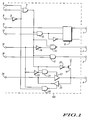
- These external lines or buses include an external address bus 1 providing an external address signal EXT_ADDR, an external read/write bus 2 providing an external read/write signal EXT_RW, an external clock line 3 providing an external clock signal EXT_E, and an external data bus 4 providing an external data signal EXT_DATA, which can be either read from or written to the external data bus 4 depending on the external read/write signal EXT_RW.
- an OR gate 5 has three inputs.
- a first input 6 is a reset signal RESET, which is used when the microcontroller is being initiated to prevent the external lines and buses from being frozen so that they are intialised.
- a second input 7 is a signal FREEZ_DIS, which is used to selectively disable the freeze operation if it is desired to operate the microcontroller with the external buses and lines always active.
- the third input 8 is a signal IMMP is provided in the microcontroller to indicate whether the lines or buses to be activated are internal or external. This signal IMMP is usually at level "1" when the activity is internal, so the signal IMMP is passed through an inverter 9 before being passed to the OR gate 5.
- the OR gate 5 gives a "1" output if any of the inputs are “1", so that if the microcontroller is being reset or if the freeze mode is disabled or if activity is on the external buses or lines, then the output signal FRIMB of the OR gate 5 is a "1".
- the external address bus 1 is coupled to an internal address bus 11 via a latch 10, which, in effect, is composed of half a flip-flop.
- the internal address bus 11 is coupled to a D port of the latch and the external address bus 1 is coupled to a Q port of the latch.
- the latch has a further port C and has the property that port D is coupled to port Q when the signal input to port C is "1", but that ports D and Q are uncoupled when the signal at port C is "0".
- the latch 10 When the external address bus 1 is to be used, it is desired that the latch 10 be “transparent" so that the same value is on both the internal address bus 11 and the external address bus 1. However, when the external address bus 1 is to be frozen, or made inactive, then the latch 10 is required to retain the previous value on the buses 1 and 11.
- the output signal FRIMB from the OR gate 5 is used as one input to an AND gate 12, whose other input is an address clock signal ADDR_STROB from an address clock line 13.
- the output of the AND gate 12 is therefore "1" only when both signals FRIMB and ADDR_STROB are "1", that is when the activity is external or freeze is disabled or the status is in reset mode and the address clock is in on phase.
- the output "1" of the AND gate 12 is passed to the C port of latch 10 and the ports D and Q are coupled. If the output of the AND gate 12 is "0", then the ports D and Q are decoupled so that the external address bus 1 is effectively frozen.
- the output signal from the AND gate 12 is also passed via an inverter 13 to an inverse C port of latch 10.
- An internal read/write bus 14 has an internal read/write signal INT_RW, which is a "1" for READ and a "0" for WRITE. This internal read/write signal INT_RW is thus used, via an inverter 16, as one input to a NAND gate 15, whose other input is the output signal FRIMB from the OR gate 5.
- the external clock line 3, which provides the external clock signal EXT_E is coupled to the output of an AND gate 17 having one input coupled to receive the output signal FRIMB from the OR gate 5 and the other input coupled to receive an internal clock signal INT_E from an internal clock line 18.
- the output signal FRIMB from the OR gate 5 is a "1"
- the external clock signal EXT_E will mimic the internal clock signal INT_E.
- the external data bus 4 is coupled to one current electrode of a transistor 19 , whose other current electrode is coupled to a positive voltage reference V dd .
- the transistor 19 has a weak resistance to provide a well defined voltage level for the external data bus 4 when it is frozen.
- the transistor 19 therefore has its control electrode coupled to receive the output signal FRIMB from the OR gate 5 via an inverter 20 so that the transistor 19 is switched “on” when output signal FRIMB from the OR gate 5 is a "0", that is, if the activity is internal and freeze is not disabled and the status is not in reset mode.
- the output signal FRIMB from the OR gate 5 is also passed to one input of an AND gate 21, whose other input is the internal read/write signal INT_RW from the internal read/write bus 14 via an inverter 22.
- the output signal FRIMB from the OR gate 5 is a "1"
- the output of the AND gate 21 will be a "1”.
- the output of the AND gate 21 is used to control a tristate buffer 23 in the external write path between an internal data bus 24 providing an internal data signal INT_DATA to be written onto the external data bus 4 as an external data signal EXT_DATA.
- the output od AND gate 21 is a "1"
- the tristate buffer 23 is enabled , thus activating the write path.
- a further truistate buffer 25 is provided in the read path.
- This buffer 25 is controlled by the output of AND gate 26 whose inputs are the internal read/write signal INT_RW from the internal read/write bus 14 and the inverted IMMP signal from inverter 9.
- the tristate buffer 25 is enabled, activating the read path.
- the AND gate 26 does not receive the output signal FRIMB from the OR gate 5, but only the inverted IMMP signal from inverter 9, since for a read operation, neither the RESET signal, which is used when the microcontroller is being initiated to prevent the external lines and buses from being frozen so that they are intialised, nor the FREEZ_DIS signal, which is used to selectively disable the freeze operation, are appropriate.
Landscapes
- Engineering & Computer Science (AREA)
- Theoretical Computer Science (AREA)
- Physics & Mathematics (AREA)
- General Engineering & Computer Science (AREA)
- General Physics & Mathematics (AREA)
- Software Systems (AREA)
- Microcomputers (AREA)
- Bus Control (AREA)
Applications Claiming Priority (2)
| Application Number | Priority Date | Filing Date | Title |
|---|---|---|---|
| GB9418226 | 1994-09-09 | ||
| GB9418226A GB2294339A (en) | 1994-09-09 | 1994-09-09 | Power-saving in an expanded mode microcontroller |
Publications (1)
| Publication Number | Publication Date |
|---|---|
| EP0701193A1 true EP0701193A1 (fr) | 1996-03-13 |
Family
ID=10761116
Family Applications (1)
| Application Number | Title | Priority Date | Filing Date |
|---|---|---|---|
| EP95112908A Withdrawn EP0701193A1 (fr) | 1994-09-09 | 1995-08-17 | MicrocontrÔleur à mode étendu |
Country Status (6)
| Country | Link |
|---|---|
| EP (1) | EP0701193A1 (fr) |
| JP (1) | JPH0887486A (fr) |
| KR (1) | KR960011682A (fr) |
| CN (1) | CN1139778A (fr) |
| GB (1) | GB2294339A (fr) |
| SG (1) | SG38873A1 (fr) |
Citations (1)
| Publication number | Priority date | Publication date | Assignee | Title |
|---|---|---|---|---|
| DE4201133A1 (de) * | 1991-01-18 | 1992-07-30 | Mitsubishi Electric Corp | Mikrocomputersystem |
Family Cites Families (2)
| Publication number | Priority date | Publication date | Assignee | Title |
|---|---|---|---|---|
| GB2228348A (en) * | 1989-01-13 | 1990-08-22 | Texas Instruments Ltd | Memory interface integrated circuit |
| JP3529805B2 (ja) * | 1992-03-27 | 2004-05-24 | ナショナル・セミコンダクター・コーポレイション | ハードウェア制御パワー管理機能と選択可能な入出力制御ピンとを有するマイクロプロセッサ |
-
1994
- 1994-09-09 GB GB9418226A patent/GB2294339A/en not_active Withdrawn
-
1995
- 1995-08-17 EP EP95112908A patent/EP0701193A1/fr not_active Withdrawn
- 1995-08-23 JP JP7235924A patent/JPH0887486A/ja active Pending
- 1995-09-06 CN CN95116199A patent/CN1139778A/zh active Pending
- 1995-09-06 SG SG1995001290A patent/SG38873A1/en unknown
- 1995-09-07 KR KR1019950029653A patent/KR960011682A/ko not_active Withdrawn
Patent Citations (1)
| Publication number | Priority date | Publication date | Assignee | Title |
|---|---|---|---|---|
| DE4201133A1 (de) * | 1991-01-18 | 1992-07-30 | Mitsubishi Electric Corp | Mikrocomputersystem |
Non-Patent Citations (1)
| Title |
|---|
| YISHAY ET AL: "To Drive or not to Drive External Pins While in Low Power Stop Mode", MOTOROLA TECHNICAL DEVELOPMENTS, vol. 21, SCHAUMBURG, ILLINOIS US, pages 92 - 93 * |
Also Published As
| Publication number | Publication date |
|---|---|
| JPH0887486A (ja) | 1996-04-02 |
| SG38873A1 (en) | 1997-04-17 |
| CN1139778A (zh) | 1997-01-08 |
| KR960011682A (ko) | 1996-04-20 |
| GB2294339A (en) | 1996-04-24 |
| GB9418226D0 (en) | 1994-10-26 |
Similar Documents
| Publication | Publication Date | Title |
|---|---|---|
| US5834947A (en) | Microcontroller accessible macrocell | |
| US4349870A (en) | Microcomputer with programmable multi-function port | |
| US5600597A (en) | Register protection structure for FPGA | |
| US5276889A (en) | Microprocessor having built-in synchronous memory with power-saving feature | |
| EP0178163B1 (fr) | Dispositif de mémoire numérique à double accès | |
| JP3954238B2 (ja) | レジスタファイル | |
| KR960018880A (ko) | 배경 모드에서 투명 동작을 갖는 데이타 처리기 및 그 방법 | |
| KR0142033B1 (ko) | 마이크로 컴퓨터 | |
| US5442775A (en) | Two clock microprocessor design with stall | |
| US6205514B1 (en) | Synchronous SRAM having global write enable | |
| EP0701193A1 (fr) | MicrocontrÔleur à mode étendu | |
| US6034545A (en) | Macrocell for data processing circuit | |
| EP0660330A2 (fr) | Méthode et système de traitement d'information ayant une mémoire pouvant opérer dans un mode de faible puissance | |
| US6275420B1 (en) | Semiconductor device having memory cell part and transfer circuit | |
| US6127850A (en) | Low power clock buffer with shared, clocked transistor | |
| JP4190593B2 (ja) | バス上の容量結合を補償する補償回路を有するデータ処理システム | |
| JP2552316B2 (ja) | Cmos半導体集積回路 | |
| US20030188209A1 (en) | Control circuit, electronic circuit, and method of saving power | |
| JPH10188567A (ja) | メモリ及びマイコン | |
| US5862408A (en) | Microprocessor system having multiplexor disposed in first and second read paths between memory CPU and DMA for selecting data from either read path | |
| KR920003271B1 (ko) | 마이컴의 제어에 의한 메모리 라이트 방지회로 | |
| JPH04227327A (ja) | 低消費電力型プログラマブルロジックアレイおよびそれを用いた情報処理装置 | |
| JPH0787239B2 (ja) | メモリ | |
| US6154820A (en) | Arrangement for storing program instructions and data in a memory device and method therefor | |
| KR100257078B1 (ko) | 내부회로와 주변회로의 인터페이스 장치 |
Legal Events
| Date | Code | Title | Description |
|---|---|---|---|
| PUAI | Public reference made under article 153(3) epc to a published international application that has entered the european phase |
Free format text: ORIGINAL CODE: 0009012 |
|
| AK | Designated contracting states |
Kind code of ref document: A1 Designated state(s): DE FR IT |
|
| 17P | Request for examination filed |
Effective date: 19960913 |
|
| 17Q | First examination report despatched |
Effective date: 19980205 |
|
| STAA | Information on the status of an ep patent application or granted ep patent |
Free format text: STATUS: THE APPLICATION IS DEEMED TO BE WITHDRAWN |
|
| 18D | Application deemed to be withdrawn |
Effective date: 19980818 |