EP0701328A2 - Feldprogrammierbare Gatteranordnung - Google Patents
Feldprogrammierbare Gatteranordnung Download PDFInfo
- Publication number
- EP0701328A2 EP0701328A2 EP95306055A EP95306055A EP0701328A2 EP 0701328 A2 EP0701328 A2 EP 0701328A2 EP 95306055 A EP95306055 A EP 95306055A EP 95306055 A EP95306055 A EP 95306055A EP 0701328 A2 EP0701328 A2 EP 0701328A2
- Authority
- EP
- European Patent Office
- Prior art keywords
- multiplexer
- circuit
- decoder circuit
- output terminal
- recited
- Prior art date
- Legal status (The legal status is an assumption and is not a legal conclusion. Google has not performed a legal analysis and makes no representation as to the accuracy of the status listed.)
- Withdrawn
Links
Images



Classifications
-
- H—ELECTRICITY
- H03—ELECTRONIC CIRCUITRY
- H03K—PULSE TECHNIQUE
- H03K19/00—Logic circuits, i.e. having at least two inputs acting on one output; Inverting circuits
- H03K19/02—Logic circuits, i.e. having at least two inputs acting on one output; Inverting circuits using specified components
- H03K19/173—Logic circuits, i.e. having at least two inputs acting on one output; Inverting circuits using specified components using elementary logic circuits as components
- H03K19/177—Logic circuits, i.e. having at least two inputs acting on one output; Inverting circuits using specified components using elementary logic circuits as components arranged in matrix form
-
- H—ELECTRICITY
- H03—ELECTRONIC CIRCUITRY
- H03K—PULSE TECHNIQUE
- H03K19/00—Logic circuits, i.e. having at least two inputs acting on one output; Inverting circuits
- H03K19/02—Logic circuits, i.e. having at least two inputs acting on one output; Inverting circuits using specified components
- H03K19/173—Logic circuits, i.e. having at least two inputs acting on one output; Inverting circuits using specified components using elementary logic circuits as components
- H03K19/1733—Controllable logic circuits
- H03K19/1737—Controllable logic circuits using multiplexers
-
- H—ELECTRICITY
- H03—ELECTRONIC CIRCUITRY
- H03K—PULSE TECHNIQUE
- H03K19/00—Logic circuits, i.e. having at least two inputs acting on one output; Inverting circuits
- H03K19/02—Logic circuits, i.e. having at least two inputs acting on one output; Inverting circuits using specified components
- H03K19/173—Logic circuits, i.e. having at least two inputs acting on one output; Inverting circuits using specified components using elementary logic circuits as components
- H03K19/177—Logic circuits, i.e. having at least two inputs acting on one output; Inverting circuits using specified components using elementary logic circuits as components arranged in matrix form
- H03K19/17704—Logic circuits, i.e. having at least two inputs acting on one output; Inverting circuits using specified components using elementary logic circuits as components arranged in matrix form the logic functions being realised by the interconnection of rows and columns
Definitions
- the present invention relates to programmable logic devices formed in integrated circuit semiconductor chips. More particularly, the invention relates to logic cells which are part of field programmable gate array chips.
- Integrated circuits have traditionally implemented a single function, or functions that were defined by software programming. However, in either case, the logic architecture that implemented the functionality was fixed during the design of the IC. More recently, integrated circuits have been developed whose logic architecture can be changed after manufacture. For example, Field Programmable Gate Arrays (FPGAs) have been developed whose logic functions can be established by the user. Typically, the logic functions are implemented in Programmable Function Units (PFUs) which generally includes various logic circuit elements (AND gates, OR gates, NAND gates, NOR gates, flip-flops, lookup table memory, multiplexers, registers, latches, and tri-state buffers, for example) that may be connected in a desired arrangement in order to implement desired logic and memory functions.
- PFUs Programmable Function Units
- typical logic functions include combinational logic, adders, counters, and other data path functions.
- the combinational logic is typically performed using Look-up tables (LUTs), whereas sequential logic is typically performed using storage elements (registers) such as flip-flops and latches.
- LUTs Look-up tables
- sequential logic is typically performed using storage elements (registers) such as flip-flops and latches.
- each logic cell (or PLC: programmable logic cell) utilizes Look-up Tables (LUTs) to implement combinational logic functions.
- LUTs employ Static random access memory's (RAMs) to implement the Boolean functions in accordance with the combinational logic function of each PLC.
- RAMs Static random access memory's
- K is to denote the maximum number of inputs which can be coupled to a Boolean network and can be implemented by an individual PLC of an FPGA.
- FIG. 1 illustrates a prior art block diagram of a LUT 152 of a PLC 150.
- FIG. 1 illustrates a prior art block diagram of a LUT 152 of a PLC 150.
- LUT 152 is a 16-bit RAM which enables PLC 150 to implement a Boolean function of up to four inputs (e.g., K
- the particular size (RAM) of the LUTs and their circuit configuration in a PLC determine the K value for the particular PLC.
- the aforementioned PLC 150 (FIG. 2) is provided with 16-bit RAM F and G LUTS 162 and 164 of a combined size of 32 bits providing a K value of five.
- the aforementioned PLC 170 (FIG. 3) has the identical 16-bit RAM F and G LUTS of a combined size of 32 bits providing a K value of eight (since the inputs (A1 to A4 and A6 to A9) of F and G LUTS were independent of one another).
- an extra LUT may be added to the output terminals of F and G LUTS 162 and 164 in order to raise the K value.
- the added H-LUT 172 in the PLC 170 (FIG. 3) functioned to increase the value of K by one.
- adding additional LUTS to a PLC increases signal propagation time (e.g., decreases the circuit speed), which is disadvantageous for most circuit applications.
- an increase in the number of PLC levels in a FPGA correspondingly increases both the size and cost of the FPGA.
- the present invention is directed towards a field programmable gate array integrated circuit having a multiplicity of PLCs, wherein each PLC includes a decoder circuit arrangement operative to increase the numbers of inputs (K) to each PLC.
- the decoder circuit arrangement is preferably coupled to each LUT of each PLC, whereby the number of inputs to the PLC is increased by the corresponding number of inputs of the aforementioned decoder circuit arrangement.
- Each decoder circuit arrangement preferably includes a multiplexer circuit coupled to a LUT of a PLC. Further provided is a decoder circuit having a plurality of input terminals with its output terminal connected to the address selector of the multiplexer circuit.
- the multiplexer circuit includes a 2 to 1 MUX having its first input terminal coupled to an output terminal of a LUT and its second input terminal connected to a default value. The address selector of the 2 to 1 MUX is coupled to and controlled by the aforementioned decoder circuit.
- the decoder circuit arrangement of the present invention increases the power of each PLC by increasing the maximum number of inputs (K) for the Boolean network associated with the FPGA without necessitating the need to add additional layers of LUTs to the circuitry FPGA.
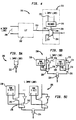
- FIG. 4 illustrates a portion of a programmable logic cell (PLC) 200 including a look-up table (LUT) 202 coupled to the decoder circuit arrangement 203 of the present invention.
- the decoder circuit arrangement 203 in its simplest embodiment includes a multiplexer (MUX) 204 and a conventional decoder circuit 206.
- MUX multiplexer
- PLC 200 may be implemented into the integrated circuitry of commercially available FPGAs, such as the ORCA FPGA, commercially available from AT&T.
- the provision of the decoder circuit arrangement 203 to a PLC 200 is functional to increase the number of inputs (K) to a PLC 200 without the aforementioned disadvantages associated with adding additional layers of LUT circuitry.
- K m inputs
- the output line 210 of LUT 202 is coupled to a first input terminal 212 of preferably a 2 to 1 MUX 204.
- the second input 214 terminal of MUX 204 is coupled to a default value (0).
- the address selector terminal 218 of MUX 204 is coupled to the decoder circuit 206.
- a decoder circuit 206 is a device for translating a combination of input signals into one output signal representative of the input combinational signal.
- decoder circuit 206 is adapted to have L input lines 220. Therefore, the decoder circuit 206 is operative to have either an logic high (1) or logic low (0) output at its output terminal (line 220) in dependence upon the combinational values of the L inputs 220. It is to be appreciated by one skilled in the art that the translation scheme of the decoder circuit 206 may be readily configured to have a logic high (1) or logic low (0) output value in dependence upon particular input combinational values to the decoder circuit 206.
- the value inputted (e.g., 0 to 1) to address selector 218 of MUX 204 is determinative to select which input terminal (212 or 214) is to be coupled to the output terminal Y.
- MUX 204 is adapted to be active low (0), whereby when the output (line 220) of decoder circuit 206 is logic low (0) the first input terminal 212 of MUX 204 is coupled to its output Y.
- the Y output value of MUX 204 equals the output value of LUT 202, via output line 210.
- the output of decoder circuit 206 is logic high (1), the Y output value of MUX 204 is equal to the default value (0) of the second input terminal 214.
- the decoder circuit arrangement 203 is operative to increase the number of inputs (K) to PLC 200 by a factor of (L).
- FIGS. 5a to 5c there is illustrated alternative preferred embodiments for the decoder circuit 206 of FIG. 4.
- FIG. 5a illustrates the decoder circuit 206 having the configuration of a conventional NAND gate 222 having L input terminals.
- FIG. 5b illustrates the decoder circuit 206 in the configuration of a NAND gate 224 having L input terminals, wherein each input terminal is coupled to a 2 to 1 MUX 226.
- Each 2 to 1 MUX 226 has its respective input terminals 228, 230 associated with a common node 232, wherein intermediate node 232 and input terminal 230 is a conventional inverter 234.
- the address selector 236 of MUX 226 is coupled to and controlled by a 1-bit static random access memory (RAM) 238.
- FIG. 5c illustrates the MUX 226 of FIG. 5b comprised of first and second transistors 240 and 242, wherein the base of each respective transistor 240, 242 is coupled to the 1-bit static RAM 238 so as to be activated or de-activated thereby.
- the decoder circuit 206 of FIG. 4 may be configured in numerous circuit schemes, (e.g., NAND gate 224 may be replaced with an AND gate) and is not to be limited to those illustrated in FIG. 5.
- FIG. 6 illustrates yet another preferred embodiment of a decoder circuit arrangement 245 in a PLC 250 in accordance with the present invention.
- Decoder circuit arrangement 245 is substantially similar to decoder circuit arrangement 203 of FIG. 4, with the exception that the second input terminal 214 of MUX 204 is coupled to a 1-bit static RAM 252. The provision of RAM 252 enables a user to adapt MUX 204 to have a default value of either 0 or 1.
- the outputs of each LUT 302 and 304 are respectively coupled to a 2 to 1 MUX 306, via lines 308, 310.
- the output of MUX 306 is coupled to the first input terminal 212 of the aforementioned MUX 204, via line 312.
- the aforementioned decoder circuit arrangement 245 is enabled to cooperatively function with the PLC 300 of the ORCA FAGA, and as mentioned above, decoder circuit arrangement 245 is operative to increase the number of inputs to PLC 300 by L (the number of inputs to the decoder circuit 206) .
- L the number of inputs to the decoder circuit 206 .
- PLC 350 is substantially similar to PLC 300 of FIG. 7, with the exception that PLC 350 is provided with a 4 to 1 MUX 360 in contrast to the two 2 to 1 MUXs 306, 204 of PLC 300 of FIG. 7.
- PLC 350 includes the aforementioned 16-bit LUTs 302, 304, wherein the respective outputs of LUTs (lines 303 and 305) 302, 304 are respectively inputted to first and second inputs terminals 362, 364 of MUX 360, via lines 352, 354.
- the L-input decoder circuit 206 is coupled to a first address selector terminal 372 of MUX 360, and input terminals 366 and 368 of MUX 360 are coupled to a 1-bit static RAM 373 which is operative to provide a default value of either 0 or 1.
- the output (Y) of MUX 360 is selected from either the output value of LUT 302 or LUT 304, via input terminals 362, 364 in dependence upon the value inputted into the second address selector terminal 374. Therefore, the output (Y) of MUX 360 has the value of either LUT 302 or LUT 304. If the output of the decoder circuit 206 is inactive (1), then the output (Y) of MUX 360 equates with the output of RAM 373, via input terminals 366, 368.
- each decoder circuit arrangement employed in a particular PLC is effective to correspondingly increase the number of inputs (K) to that particular PLC.
- TABLE A an 8-input combinational logic function is illustrated in TABLE A. It is to be appreciated by one skilled in the art that this function typically has too many variables for intended applications, and consequently it must be "decomposed" into a set of smaller functions.
- TABLE B illustrates three (3) smaller combinational functions produced by commercially avaible software, such as SIS 1 1 from U.C. Berkley. It is noted that the combination of the three (3) functions illustrated in TABLE B is logically equivalent to the function illustrated in TABLE A as shown hereinbelow.
- the tmp1 and tmp2 cover outputs are respectively inputted into LUTs T3 and T2 (406) of PLC 420, wherein LUTs T3 and T2 (406) are also provided with three additional inputs (a2, a4, a8).
- LUTs T3 and T2 (406) of PLC 420 provide the 'y' cover output (line 422).
- the aforementioned FPGA circuit arrangement of FIG. 9 required two levels of PLCs 400, 420 to implement the 'y' cover having eight inputs. Therefore, the aforementioned input signals (al thru a8) were required to be processed by two levels of PLCs 400 420 before the 'y' cover output signal is generated.
- the additional PLC 420 level effects an increase in the overall size of the FPGA required to accommodate PLC 420, as well as an increase in the signal propagation time and cost for the FPGA.
- FIG. 10 illustrates a PLC 450 of the aforementioned AT&T ORCA FPGA implementing the decoder circuit arrangement of the present invention.
- the 'tmp 1' output from LUTs T3 and T2 (452) is coupled to a 2 to 1 MUX 456 while the 'tmp 2' output from LUTs T1 and T0 (454) is coupled to a second 2 to 1 MUX 458.
- MUX 456 has its address selector 457 coupled to decoder circuit 460, while MUX 458 has its address selector 459 coupled to decoder circuit 462.
- the outputs (lines 470 and 472) of each MUX 458, 460 are respectively coupled to a NAND gate 464 whose output provides the 'y' cover.
- decoder circuit 460 is adapted to be active low (0) when inputs a2, a4 and a8 are respectively 010
- decoder circuit 462 is adapted to be active low (0) when inputs a2, a4 and a8 are respectively 101.
- the FPGA circuit arrangement of FIG. 10 achieves such identical results by employing only one PLC 450, in contrast to the two PLCs 400, 420 required for the aforementioned prior art FPGA circuit arrangement of FIG. 9.
- the present invention FPGA circuit arrangement (FIG. 10) is advantageous in that it requires less overall size, reduces delay time (input signals need only be processed in one PLC 450), and reduces the cost of circuitry in comparison to a prior art FPGA circuit arrangement requiring two levels of PLCs 400 and 420.
Landscapes
- Physics & Mathematics (AREA)
- Mathematical Physics (AREA)
- Engineering & Computer Science (AREA)
- Computer Hardware Design (AREA)
- Computing Systems (AREA)
- General Engineering & Computer Science (AREA)
- Logic Circuits (AREA)
- Static Random-Access Memory (AREA)
- Design And Manufacture Of Integrated Circuits (AREA)
Applications Claiming Priority (2)
| Application Number | Priority Date | Filing Date | Title |
|---|---|---|---|
| US08/304,013 US5442306A (en) | 1994-09-09 | 1994-09-09 | Field programmable gate array using look-up tables, multiplexers and decoders |
| US304013 | 2002-11-26 |
Publications (2)
| Publication Number | Publication Date |
|---|---|
| EP0701328A2 true EP0701328A2 (de) | 1996-03-13 |
| EP0701328A3 EP0701328A3 (de) | 1997-07-09 |
Family
ID=23174653
Family Applications (1)
| Application Number | Title | Priority Date | Filing Date |
|---|---|---|---|
| EP95306055A Withdrawn EP0701328A3 (de) | 1994-09-09 | 1995-08-30 | Feldprogrammierbare Gatteranordnung |
Country Status (3)
| Country | Link |
|---|---|
| US (1) | US5442306A (de) |
| EP (1) | EP0701328A3 (de) |
| JP (1) | JPH08237109A (de) |
Cited By (3)
| Publication number | Priority date | Publication date | Assignee | Title |
|---|---|---|---|---|
| EP1447910A3 (de) * | 2003-02-11 | 2005-09-21 | Altera Corporation | Eine teilbare, unvollständige Nachschlagstabelle für flächeneffiziente, logische Elemente |
| US7386812B2 (en) | 2003-11-21 | 2008-06-10 | Infineon Technologies Ag | Logic basic cell and logic basic cell arrangement |
| EP4318254A1 (de) | 2022-08-05 | 2024-02-07 | Fraunhofer-Gesellschaft zur Förderung der angewandten Forschung e.V. | Halbleitervorrichtungssystem |
Families Citing this family (31)
| Publication number | Priority date | Publication date | Assignee | Title |
|---|---|---|---|---|
| US5596742A (en) * | 1993-04-02 | 1997-01-21 | Massachusetts Institute Of Technology | Virtual interconnections for reconfigurable logic systems |
| US5761484A (en) * | 1994-04-01 | 1998-06-02 | Massachusetts Institute Of Technology | Virtual interconnections for reconfigurable logic systems |
| US5659716A (en) * | 1994-11-23 | 1997-08-19 | Virtual Machine Works, Inc. | Pipe-lined static router and scheduler for configurable logic system performing simultaneous communications and computation |
| US5742180A (en) * | 1995-02-10 | 1998-04-21 | Massachusetts Institute Of Technology | Dynamically programmable gate array with multiple contexts |
| US5528169A (en) * | 1995-04-26 | 1996-06-18 | Xilinx, Inc. | Method and structure for providing a flip flop circuit with a configurable data input path |
| US5559450A (en) * | 1995-07-27 | 1996-09-24 | Lucent Technologies Inc. | Field programmable gate array with multi-port RAM |
| JPH0983348A (ja) * | 1995-09-14 | 1997-03-28 | Hitachi Ltd | 可変論理回路 |
| US6107822A (en) * | 1996-04-09 | 2000-08-22 | Altera Corporation | Logic element for a programmable logic integrated circuit |
| US5894565A (en) * | 1996-05-20 | 1999-04-13 | Atmel Corporation | Field programmable gate array with distributed RAM and increased cell utilization |
| US6297665B1 (en) | 1996-11-22 | 2001-10-02 | Xilinx, Inc. | FPGA architecture with dual-port deep look-up table RAMS |
| US5889413A (en) * | 1996-11-22 | 1999-03-30 | Xilinx, Inc. | Lookup tables which double as shift registers |
| US6323682B1 (en) | 1996-11-22 | 2001-11-27 | Xilinx, Inc. | FPGA architecture with wide function multiplexers |
| US6288568B1 (en) | 1996-11-22 | 2001-09-11 | Xilinx, Inc. | FPGA architecture with deep look-up table RAMs |
| US6084427A (en) | 1998-05-19 | 2000-07-04 | Altera Corporation | Programmable logic devices with enhanced multiplexing capabilities |
| US6191611B1 (en) * | 1997-10-16 | 2001-02-20 | Altera Corporation | Driver circuitry for programmable logic devices with hierarchical interconnection resources |
| US6353920B1 (en) * | 1998-11-17 | 2002-03-05 | Xilinx, Inc. | Method for implementing wide gates and tristate buffers using FPGA carry logic |
| US6407576B1 (en) * | 1999-03-04 | 2002-06-18 | Altera Corporation | Interconnection and input/output resources for programmable logic integrated circuit devices |
| WO2000052826A2 (en) * | 1999-03-04 | 2000-09-08 | Altera Corporation | Interconnection and input/output resources for programmable logic integrated circuit devices |
| US6294926B1 (en) * | 1999-07-16 | 2001-09-25 | Philips Electronics North America Corporation | Very fine-grain field programmable gate array architecture and circuitry |
| US6724810B1 (en) | 2000-11-17 | 2004-04-20 | Xilinx, Inc. | Method and apparatus for de-spreading spread spectrum signals |
| US6577678B2 (en) | 2001-05-08 | 2003-06-10 | Quicksilver Technology | Method and system for reconfigurable channel coding |
| JP3580785B2 (ja) * | 2001-06-29 | 2004-10-27 | 株式会社半導体理工学研究センター | ルックアップテーブル、ルックアップテーブルを備えるプログラマブル論理回路装置、および、ルックアップテーブルの構成方法 |
| JP4213044B2 (ja) * | 2002-03-18 | 2009-01-21 | エヌエックスピー ビー ヴィ | Lutベースのリコンフィギュラブル・ロジック・アーキテクチャのためのコンフィギュレーション・メモリの実装 |
| JP4260026B2 (ja) | 2002-03-18 | 2009-04-30 | エヌエックスピー ビー ヴィ | リコンフィギャラブル・ロジックにおける大型マルチプレクサの実現 |
| US7002370B1 (en) * | 2003-12-04 | 2006-02-21 | Altera Corporation | Multiplexer configuration for programmable logic device |
| US7379777B2 (en) * | 2006-01-24 | 2008-05-27 | National Instruments Corporation | System and method for automatically updating the memory map of a programmable logic controller to customized hardware |
| US7904761B1 (en) * | 2006-03-24 | 2011-03-08 | Xilinx, Inc. | Method and apparatus for a discrete power series generator |
| US9336051B2 (en) * | 2007-10-19 | 2016-05-10 | National Instruments Corporation | Programmable controller with multiple processors using a scanning architecture |
| US20090106755A1 (en) * | 2007-10-19 | 2009-04-23 | Sundeep Chandhoke | Programmable Controller with Multiple Processors Using Scanning and Data Acquisition Architectures |
| US11070358B2 (en) | 2015-12-15 | 2021-07-20 | Koninklijke Philips N.V. | Computation device and method |
| US9705504B1 (en) | 2016-01-13 | 2017-07-11 | Altera Corporation | Power gated lookup table circuitry |
Family Cites Families (16)
| Publication number | Priority date | Publication date | Assignee | Title |
|---|---|---|---|---|
| US4706216A (en) * | 1985-02-27 | 1987-11-10 | Xilinx, Inc. | Configurable logic element |
| US4831573A (en) * | 1987-03-06 | 1989-05-16 | Altera Corporation | Programmable integrated circuit micro-sequencer device |
| JP2879070B2 (ja) * | 1989-02-15 | 1999-04-05 | コーニンクレッカ フィリップス エレクトロニクス エヌ ヴィ | プログラム可能論理ユニット及び信号プロセッサ |
| US4940909A (en) * | 1989-05-12 | 1990-07-10 | Plus Logic, Inc. | Configuration control circuit for programmable logic devices |
| US5313119A (en) * | 1991-03-18 | 1994-05-17 | Crosspoint Solutions, Inc. | Field programmable gate array |
| US5260610A (en) * | 1991-09-03 | 1993-11-09 | Altera Corporation | Programmable logic element interconnections for programmable logic array integrated circuits |
| US5208491A (en) * | 1992-01-07 | 1993-05-04 | Washington Research Foundation | Field programmable gate array |
| US5237219A (en) * | 1992-05-08 | 1993-08-17 | Altera Corporation | Methods and apparatus for programming cellular programmable logic integrated circuits |
| US5291079A (en) * | 1992-07-23 | 1994-03-01 | Xilinx, Inc. | Configuration control unit for programming a field programmable gate array and reading array status |
| US5317698A (en) * | 1992-08-18 | 1994-05-31 | Actel Corporation | FPGA architecture including direct logic function circuit to I/O interconnections |
| GB9303084D0 (en) * | 1993-02-16 | 1993-03-31 | Inmos Ltd | Programmable logic circuit |
| US5317212A (en) * | 1993-03-19 | 1994-05-31 | Wahlstrom Sven E | Dynamic control of configurable logic |
| US5311080A (en) * | 1993-03-26 | 1994-05-10 | At&T Bell Laboratories | Field programmable gate array with direct input/output connection |
| US5381058A (en) * | 1993-05-21 | 1995-01-10 | At&T Corp. | FPGA having PFU with programmable output driver inputs |
| US5352940A (en) * | 1993-05-27 | 1994-10-04 | Altera Corporation | Ram convertible look-up table based macrocell for PLDs |
| US5349250A (en) * | 1993-09-02 | 1994-09-20 | Xilinx, Inc. | Logic structure and circuit for fast carry |
-
1994
- 1994-09-09 US US08/304,013 patent/US5442306A/en not_active Expired - Lifetime
-
1995
- 1995-08-30 EP EP95306055A patent/EP0701328A3/de not_active Withdrawn
- 1995-09-08 JP JP7230833A patent/JPH08237109A/ja not_active Withdrawn
Non-Patent Citations (1)
| Title |
|---|
| None |
Cited By (5)
| Publication number | Priority date | Publication date | Assignee | Title |
|---|---|---|---|---|
| EP1447910A3 (de) * | 2003-02-11 | 2005-09-21 | Altera Corporation | Eine teilbare, unvollständige Nachschlagstabelle für flächeneffiziente, logische Elemente |
| US7030650B1 (en) | 2003-02-11 | 2006-04-18 | Altera Corporation | Fracturable incomplete look up table area efficient logic elements |
| US7386812B2 (en) | 2003-11-21 | 2008-06-10 | Infineon Technologies Ag | Logic basic cell and logic basic cell arrangement |
| DE102004056322B4 (de) * | 2003-11-21 | 2012-07-19 | Infineon Technologies Ag | Logik-Grundzelle und Logik-Grundzellen-Anordnung |
| EP4318254A1 (de) | 2022-08-05 | 2024-02-07 | Fraunhofer-Gesellschaft zur Förderung der angewandten Forschung e.V. | Halbleitervorrichtungssystem |
Also Published As
| Publication number | Publication date |
|---|---|
| EP0701328A3 (de) | 1997-07-09 |
| JPH08237109A (ja) | 1996-09-13 |
| US5442306A (en) | 1995-08-15 |
Similar Documents
| Publication | Publication Date | Title |
|---|---|---|
| US5442306A (en) | Field programmable gate array using look-up tables, multiplexers and decoders | |
| US6556500B2 (en) | Programmable logic array device with random access memory configurable as product terms | |
| US7218133B2 (en) | Versatile logic element and logic array block | |
| US6501296B2 (en) | Logic/memory circuit having a plurality of operating modes | |
| US6809552B1 (en) | FPGA lookup table with transmission gate structure for reliable low-voltage operation | |
| US5796267A (en) | Tri-Statable input/output circuitry for programmable logic | |
| US6314550B1 (en) | Cascaded programming with multiple-purpose pins | |
| US6480025B1 (en) | Driver circuitry for programmable logic devices with hierarchical interconnection resources | |
| EP0746103B1 (de) | Integrierte Schaltungen mit programmierbaren logischen Feldern | |
| US6873182B2 (en) | Programmable logic devices having enhanced cascade functions to provide increased flexibility | |
| US20020125910A1 (en) | Configurable logic element with expander structures | |
| EP0617513A2 (de) | Programmierbare Gatteranordnung mit direkter Eingangs-/Ausgangsverbindung | |
| US20030234667A1 (en) | PLDs providing reduced delays in cascade chain circuits | |
| US5563528A (en) | Multiplexer for programmable logic device | |
| US6384625B1 (en) | Programmable logic devices with enhanced multiplexing capabilities | |
| US6294925B1 (en) | Programmable logic device | |
| US7253660B1 (en) | Multiplexing device including a hardwired multiplexer in a programmable logic device | |
| JPH09181598A (ja) | フィールドプログラマブルゲートアレイ | |
| US7696783B2 (en) | Logic modules for semiconductor integrated circuits | |
| US5821794A (en) | Clock distribution architecture and method for high speed CPLDs | |
| US5585759A (en) | Input buffer of semiconductor integrated circuit | |
| US7432736B2 (en) | Logic basic cell | |
| US5936425A (en) | Tri-statable input/output circuitry for programmable logic | |
| US20010044924A1 (en) | Logic circuit module, method for designing a semiconductor integrated circuit using the same, and semiconductor integrated circuit | |
| US5691653A (en) | Product term based programmable logic array devices with reduced control memory requirements |
Legal Events
| Date | Code | Title | Description |
|---|---|---|---|
| PUAI | Public reference made under article 153(3) epc to a published international application that has entered the european phase |
Free format text: ORIGINAL CODE: 0009012 |
|
| AK | Designated contracting states |
Kind code of ref document: A2 Designated state(s): DE FR GB IT |
|
| PUAL | Search report despatched |
Free format text: ORIGINAL CODE: 0009013 |
|
| AK | Designated contracting states |
Kind code of ref document: A3 Designated state(s): DE FR GB IT |
|
| STAA | Information on the status of an ep patent application or granted ep patent |
Free format text: STATUS: THE APPLICATION IS DEEMED TO BE WITHDRAWN |
|
| 18D | Application deemed to be withdrawn |
Effective date: 19980112 |