EP0701393A1 - Méthode de production d'un substrat à portions en saillie - Google Patents
Méthode de production d'un substrat à portions en saillie Download PDFInfo
- Publication number
- EP0701393A1 EP0701393A1 EP95420230A EP95420230A EP0701393A1 EP 0701393 A1 EP0701393 A1 EP 0701393A1 EP 95420230 A EP95420230 A EP 95420230A EP 95420230 A EP95420230 A EP 95420230A EP 0701393 A1 EP0701393 A1 EP 0701393A1
- Authority
- EP
- European Patent Office
- Prior art keywords
- substrate
- viscous material
- printing plate
- manufacturing
- projections
- Prior art date
- Legal status (The legal status is an assumption and is not a legal conclusion. Google has not performed a legal analysis and makes no representation as to the accuracy of the status listed.)
- Granted
Links
- 239000000758 substrate Substances 0.000 title claims abstract description 131
- 238000004519 manufacturing process Methods 0.000 title claims abstract description 35
- 239000011345 viscous material Substances 0.000 claims abstract description 106
- 238000007639 printing Methods 0.000 claims abstract description 104
- 238000000034 method Methods 0.000 claims abstract description 40
- 230000000149 penetrating effect Effects 0.000 claims abstract description 34
- 230000008569 process Effects 0.000 claims abstract description 15
- 230000005291 magnetic effect Effects 0.000 claims abstract description 14
- 239000003302 ferromagnetic material Substances 0.000 claims abstract description 6
- 239000000463 material Substances 0.000 claims description 21
- 238000010438 heat treatment Methods 0.000 claims description 9
- 239000002245 particle Substances 0.000 claims description 9
- 239000000126 substance Substances 0.000 claims description 7
- 239000011324 bead Substances 0.000 claims description 5
- 230000009471 action Effects 0.000 claims description 4
- 239000002612 dispersion medium Substances 0.000 claims description 4
- 230000005611 electricity Effects 0.000 claims description 3
- 238000011049 filling Methods 0.000 claims description 3
- 238000001816 cooling Methods 0.000 claims description 2
- 239000004744 fabric Substances 0.000 claims description 2
- 239000010985 leather Substances 0.000 claims description 2
- 229920001169 thermoplastic Polymers 0.000 claims description 2
- 239000004416 thermosoftening plastic Substances 0.000 claims description 2
- 229920000297 Rayon Polymers 0.000 claims 1
- 239000011810 insulating material Substances 0.000 claims 1
- 239000013528 metallic particle Substances 0.000 claims 1
- 238000007711 solidification Methods 0.000 claims 1
- 230000008023 solidification Effects 0.000 claims 1
- 229910000679 solder Inorganic materials 0.000 description 11
- 239000011521 glass Substances 0.000 description 9
- 238000005192 partition Methods 0.000 description 9
- 230000005294 ferromagnetic effect Effects 0.000 description 8
- 238000005530 etching Methods 0.000 description 6
- 230000007246 mechanism Effects 0.000 description 6
- 239000011347 resin Substances 0.000 description 6
- 229920005989 resin Polymers 0.000 description 6
- 239000000843 powder Substances 0.000 description 5
- 230000009467 reduction Effects 0.000 description 5
- XEEYBQQBJWHFJM-UHFFFAOYSA-N Iron Chemical compound [Fe] XEEYBQQBJWHFJM-UHFFFAOYSA-N 0.000 description 4
- 239000011888 foil Substances 0.000 description 4
- 230000000873 masking effect Effects 0.000 description 3
- 239000004033 plastic Substances 0.000 description 3
- 229920003023 plastic Polymers 0.000 description 3
- 238000009423 ventilation Methods 0.000 description 3
- PXHVJJICTQNCMI-UHFFFAOYSA-N Nickel Chemical compound [Ni] PXHVJJICTQNCMI-UHFFFAOYSA-N 0.000 description 2
- 230000001154 acute effect Effects 0.000 description 2
- 230000008901 benefit Effects 0.000 description 2
- 239000000919 ceramic Substances 0.000 description 2
- 238000005401 electroluminescence Methods 0.000 description 2
- 238000001704 evaporation Methods 0.000 description 2
- 238000013007 heat curing Methods 0.000 description 2
- 239000012212 insulator Substances 0.000 description 2
- 229910052742 iron Inorganic materials 0.000 description 2
- 239000004973 liquid crystal related substance Substances 0.000 description 2
- 239000000696 magnetic material Substances 0.000 description 2
- 239000012528 membrane Substances 0.000 description 2
- 239000002184 metal Substances 0.000 description 2
- 229910052751 metal Inorganic materials 0.000 description 2
- 238000007788 roughening Methods 0.000 description 2
- 229910000531 Co alloy Inorganic materials 0.000 description 1
- RYGMFSIKBFXOCR-UHFFFAOYSA-N Copper Chemical compound [Cu] RYGMFSIKBFXOCR-UHFFFAOYSA-N 0.000 description 1
- 239000004593 Epoxy Substances 0.000 description 1
- 229920000914 Metallic fiber Polymers 0.000 description 1
- 229910000990 Ni alloy Inorganic materials 0.000 description 1
- 239000004677 Nylon Substances 0.000 description 1
- 239000004372 Polyvinyl alcohol Substances 0.000 description 1
- 230000035508 accumulation Effects 0.000 description 1
- 238000009825 accumulation Methods 0.000 description 1
- 230000004913 activation Effects 0.000 description 1
- 239000000853 adhesive Substances 0.000 description 1
- 229910045601 alloy Inorganic materials 0.000 description 1
- 239000000956 alloy Substances 0.000 description 1
- -1 and the like Polymers 0.000 description 1
- 238000005422 blasting Methods 0.000 description 1
- 230000000740 bleeding effect Effects 0.000 description 1
- 229910017052 cobalt Inorganic materials 0.000 description 1
- 239000010941 cobalt Substances 0.000 description 1
- GUTLYIVDDKVIGB-UHFFFAOYSA-N cobalt atom Chemical compound [Co] GUTLYIVDDKVIGB-UHFFFAOYSA-N 0.000 description 1
- 150000001875 compounds Chemical class 0.000 description 1
- 239000004020 conductor Substances 0.000 description 1
- 229910052802 copper Inorganic materials 0.000 description 1
- 239000010949 copper Substances 0.000 description 1
- 239000006071 cream Substances 0.000 description 1
- 238000001035 drying Methods 0.000 description 1
- 239000013013 elastic material Substances 0.000 description 1
- 238000000605 extraction Methods 0.000 description 1
- 230000005307 ferromagnetism Effects 0.000 description 1
- 230000004907 flux Effects 0.000 description 1
- 238000000227 grinding Methods 0.000 description 1
- 238000007373 indentation Methods 0.000 description 1
- 238000009434 installation Methods 0.000 description 1
- 239000012774 insulation material Substances 0.000 description 1
- 239000000178 monomer Substances 0.000 description 1
- 229910052759 nickel Inorganic materials 0.000 description 1
- 229920001778 nylon Polymers 0.000 description 1
- 239000003960 organic solvent Substances 0.000 description 1
- 229920002120 photoresistant polymer Polymers 0.000 description 1
- 229920003205 poly(diphenylsiloxane) Polymers 0.000 description 1
- 229920000728 polyester Polymers 0.000 description 1
- 238000006116 polymerization reaction Methods 0.000 description 1
- 229920002451 polyvinyl alcohol Polymers 0.000 description 1
- 238000004080 punching Methods 0.000 description 1
- 230000002787 reinforcement Effects 0.000 description 1
- 238000007650 screen-printing Methods 0.000 description 1
- 238000005245 sintering Methods 0.000 description 1
- 239000002904 solvent Substances 0.000 description 1
- 239000010935 stainless steel Substances 0.000 description 1
- 229910001220 stainless steel Inorganic materials 0.000 description 1
- 229920002994 synthetic fiber Polymers 0.000 description 1
- 230000000007 visual effect Effects 0.000 description 1
Images


Classifications
-
- B—PERFORMING OPERATIONS; TRANSPORTING
- B41—PRINTING; LINING MACHINES; TYPEWRITERS; STAMPS
- B41F—PRINTING MACHINES OR PRESSES
- B41F15/00—Screen printers
- B41F15/08—Machines
-
- B—PERFORMING OPERATIONS; TRANSPORTING
- B41—PRINTING; LINING MACHINES; TYPEWRITERS; STAMPS
- B41M—PRINTING, DUPLICATING, MARKING, OR COPYING PROCESSES; COLOUR PRINTING
- B41M3/00—Printing processes to produce particular kinds of printed work, e.g. patterns
-
- B—PERFORMING OPERATIONS; TRANSPORTING
- B41—PRINTING; LINING MACHINES; TYPEWRITERS; STAMPS
- B41F—PRINTING MACHINES OR PRESSES
- B41F15/00—Screen printers
- B41F15/08—Machines
- B41F15/0804—Machines for printing sheets
- B41F15/0813—Machines for printing sheets with flat screens
- B41F15/0818—Machines for printing sheets with flat screens with a stationary screen and a moving squeegee
-
- B—PERFORMING OPERATIONS; TRANSPORTING
- B41—PRINTING; LINING MACHINES; TYPEWRITERS; STAMPS
- B41F—PRINTING MACHINES OR PRESSES
- B41F15/00—Screen printers
- B41F15/14—Details
- B41F15/16—Printing tables
-
- B—PERFORMING OPERATIONS; TRANSPORTING
- B41—PRINTING; LINING MACHINES; TYPEWRITERS; STAMPS
- B41F—PRINTING MACHINES OR PRESSES
- B41F15/00—Screen printers
- B41F15/14—Details
- B41F15/16—Printing tables
- B41F15/18—Supports for workpieces
-
- B—PERFORMING OPERATIONS; TRANSPORTING
- B41—PRINTING; LINING MACHINES; TYPEWRITERS; STAMPS
- B41F—PRINTING MACHINES OR PRESSES
- B41F15/00—Screen printers
- B41F15/14—Details
- B41F15/40—Inking units
- B41F15/42—Inking units comprising squeegees or doctors
- B41F15/426—Inking units comprising squeegees or doctors the squeegees or doctors being magnetically attracted
-
- H—ELECTRICITY
- H05—ELECTRIC TECHNIQUES NOT OTHERWISE PROVIDED FOR
- H05K—PRINTED CIRCUITS; CASINGS OR CONSTRUCTIONAL DETAILS OF ELECTRIC APPARATUS; MANUFACTURE OF ASSEMBLAGES OF ELECTRICAL COMPONENTS
- H05K3/00—Apparatus or processes for manufacturing printed circuits
- H05K3/10—Apparatus or processes for manufacturing printed circuits in which conductive material is applied to the insulating support in such a manner as to form the desired conductive pattern
- H05K3/12—Apparatus or processes for manufacturing printed circuits in which conductive material is applied to the insulating support in such a manner as to form the desired conductive pattern using thick film techniques, e.g. printing techniques to apply the conductive material or similar techniques for applying conductive paste or ink patterns
- H05K3/1216—Apparatus or processes for manufacturing printed circuits in which conductive material is applied to the insulating support in such a manner as to form the desired conductive pattern using thick film techniques, e.g. printing techniques to apply the conductive material or similar techniques for applying conductive paste or ink patterns by screen printing or stencil printing
- H05K3/1225—Screens or stencils; Holders therefor
-
- Y—GENERAL TAGGING OF NEW TECHNOLOGICAL DEVELOPMENTS; GENERAL TAGGING OF CROSS-SECTIONAL TECHNOLOGIES SPANNING OVER SEVERAL SECTIONS OF THE IPC; TECHNICAL SUBJECTS COVERED BY FORMER USPC CROSS-REFERENCE ART COLLECTIONS [XRACs] AND DIGESTS
- Y10—TECHNICAL SUBJECTS COVERED BY FORMER USPC
- Y10S—TECHNICAL SUBJECTS COVERED BY FORMER USPC CROSS-REFERENCE ART COLLECTIONS [XRACs] AND DIGESTS
- Y10S428/00—Stock material or miscellaneous articles
- Y10S428/901—Printed circuit
-
- Y—GENERAL TAGGING OF NEW TECHNOLOGICAL DEVELOPMENTS; GENERAL TAGGING OF CROSS-SECTIONAL TECHNOLOGIES SPANNING OVER SEVERAL SECTIONS OF THE IPC; TECHNICAL SUBJECTS COVERED BY FORMER USPC CROSS-REFERENCE ART COLLECTIONS [XRACs] AND DIGESTS
- Y10—TECHNICAL SUBJECTS COVERED BY FORMER USPC
- Y10T—TECHNICAL SUBJECTS COVERED BY FORMER US CLASSIFICATION
- Y10T428/00—Stock material or miscellaneous articles
- Y10T428/24—Structurally defined web or sheet [e.g., overall dimension, etc.]
- Y10T428/24355—Continuous and nonuniform or irregular surface on layer or component [e.g., roofing, etc.]
Definitions
- the invention of the present application relates to a method of production for a substrate having minute indentations on its surface for use with flat display panel back boards, printed circuit boards, and the like.
- LCD Liquid crystal displays
- ELD electroluminescence displays
- PDP plasma display panels
- VFD vacuum fluorescent displays
- a common feature in these flat display panels is the installation of insulated substrates on which a plurality of electrodes are arranged in high density.
- the electrode intervals are formed into minute partitions in order to separate the electrodes.
- Fig. 8 shows an example of the basic structure of a PDP.
- Insulated substrate (the back board) 1 is formed from glass or the like, and there are a plurality of parallel electrode grooves 4 of 100 ⁇ 200 ⁇ m in depth separated at regular 50 ⁇ m intervals formed on the upper surface.
- wire auxiliary anodes 2 are housed in parallel, and separated from each other by partitions located between the electrode grooves 4.
- a plurality of cathodes shaped in long narrow sheets extending in a direction intersecting auxiliary anodes 2 are arranged on the back board 1.
- a plurality of display anodes and a front plate are arranged on these cathodes.
- liquid crystal display LCD
- electroluminescence display ELD
- plasma display panel PDP
- vacuum fluorescent display VFD
- LCD liquid crystal display
- ELD electroluminescence display
- PDP plasma display panel
- VFD vacuum fluorescent display
- the first objective of the invention of the present application is to provide a method with a high processing accuracy for inexpensively and efficiently manufacturing substrates having minute projections.
- the invention of the present application possesses the following processes:
- a manufacturing method for a substrate having a surface with projections comprising the steps of: preparing a printing plate, with at least one part formed from a ferromagnetic material, and which has viscous material penetrating portions for forming projections on a flat surface; contacting said printing plate with the surface of a substrate; clamping said printing plate to said substrate by means of attraction by a magnetic force from behind said substrate; filling said viscous material penetrating portions of said printing plate with a viscous material for forming projections; forming from said viscous material a layer on said substrate in a shape the same as that of said projections; separating said printing plate from said substrate; and solidifying said viscous material printed onto said substrate forming projections.
- a printing plate is fixed to a substrate base by means of magnetic attraction; a viscous material is rubbed into viscous material penetrating portions of the printing plate; and even with thick printing plates are used to produce thick protrusions, the printing plate can be fixed with certainty and smudging is prevented. Consequently distortions of viscous material are not produced, printing position accuracy is high, projections of a desired shape can be easily formed with high precision and the substrate manufacturing costs can be reduced.
- the set up of the shape of the projections is formed by the viscous material penetrating portions of printing plate, freedom in the design and position of the projecting portions is high.
- said viscous material is rubbed into said viscous material penetrating portions in the surface of said printing plate by means of a squeegee which has a rubbing action.
- the printing plate after the aforementioned printing process, can be peel off the surface of the substrate by means of magnetic attraction, thereby making it possible to to stablely separate the printing plate without producing any strain, and lift printing plate exactly in the direction of the projecting portions, so that the shape of projecting portions is not damaged.
- Fig. 1 is a cross sectional view of a device used in an example of the substrate manufacturing process of the present invention.
- Fig. 2 is an enlarged cross sectional view of a section of the same embodiment showing viscous material being rubbed into the printing plate.
- Fig. 3 is an enlarged cross sectional view of a substrate with projections manufactured according to the same embodiment.
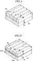
- Fig. 4 is a perspective view of a substrate with projections manufactured according to the same embodiment.
- Fig. 5 is a perspective view cf a substrate having projections manufactured according to a method of another embodiment of the invention of the present application.
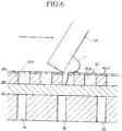
- Fig. 6 is an enlarged cross sectional view showing the process of rubbing viscous material into a printing plate according to another embodiment of the invention of the present application.
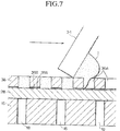
- Fig. 7 is an enlarged cross sectional view showing the process of rubbing the viscous material into a printing plate according to another embodiment of the invention of the present application.
- Fig. 8 is a perspective view showing the essential parts of a common plasma display panel.
- Fig. 1 shows a side view of an example of a printing apparatus used in the manufacturing method of the present invention for producing substrates having projections.
- an opening/closing base 12 On the upper portion of main base 10, an opening/closing base 12 is provided which is hinged at one end and can be rotated around this hinge.
- a box shaped air tight container 14 is arranged horizontally in the upper portion of main base 10. The upper surface of the air tight container 14 is covered by a rectangular substrate supporting plate 16. There are a plurality of small ventilation holes 18 formed in substrate supporting plate 16. Air tight container 14 is connected through a pipe 22 to a pressure reduction device 24. When the pressure of the inside of air tight container 14 is reduced by the action of pressure reduction device 24, air is sucked out of all the ventilation holes 18, and the substrate 28 arranged above the ventilation holes 18 can be made to adhere to the upper surface of main base 10.
- electromagnets 20 Within air tight container 14, extending across the whole lower surface of the inside of airtight container 14 are a plurality of electromagnets 20 arranged lengthwise and crosswise at fixed intervals. These electromagnets 22 are each connected to electric supply mechanism 26. When electric mechanism 26 is turned on a magnetic force is generated, and a printing plate 36 provided above substrate base 28 is attracted.
- Squeegee driving mechanism 30 is positioned along the longitudinal direction of opening/closing mechanism 12.
- a slider 32 which is movable in the above-mentioned longitudinal direction is positioned on squeegee driving mechanism 30.
- a squeegee 34 is attached perpendicularly and is tiltable on both sides at a fixed angle.
- the squeegee 34 is formed from an elastic material such as rubber with an entire length equal to the lateral width of the printing plate 36, so that when slider 32 moves, the squeegee rubs the entire area of the printing plate. At this time, squeegee 34 is tilted so as to form an acute angle with printing plate 36 in the direction of progress.
- the front side, with respect to the direction of movement, of squeegee 34 is always inclined at an acute angle to printing plate 36, thereby obtaining an action wherein viscous material I is rubbed into the viscous material penetrating portions 36A of printing plate 36.
- Printing plate 36 has a ferromagnetism extending over its whole surface, so that the shape of the projections to be formed on the flat surface of the top of substrate base 28 are formed by the viscous material penetrating portions 36A, as shown in Fig. 2.
- a plurality of partitions (projections) 40 extending in a longitudinal direction over the surface of substrate base 28, a plurality of slits 36A are formed on printing plate 36.
- the thickness of printing plate 36 determines the corresponding degree of projection of the projecting portions 40 to be formed, for example a level of 100 ⁇ m.
- the aforementioned printing plate 30B it is possible to employ (1) a printing plate formed by means of dispersing and affixing a ferromagnetic powder in a binding material, or (2) a printing plate in which openings are formed in a thin plate of a ferromagnetic substance.
- the material (1) in which a ferromagnetic powder has been dispersed and fixed in a binding material it is possible to use a resin layer formed by means of adding a ferromagnetic powder to sections other than the viscous material penetrating portion forming the print pattern of a mesh screen woven using synthetic fabric such as nylon, polyester, and the like, or metallic thread such as stainless steel thread, and the like.
- a method for forming the aforementioned resin layer a method can be appropriately employed in which a viscous material penetrating portion is formed by means of adding a ferromagnetic powder to a conventional photoresist, applying this substance to the aforementioned screen, exposing this resultant material to the reverse print pattern, and then removing unnecessary sections therein.
- any conventional ferromagnetic material may be employed such as iron, cobalt, nickel, as well as alloys of the aforementioned, oxides of magnetic materials, compounds of magnetic materials, and the like.
- the printing plate from a resin to which metallic powder has been added (including so-called “rubber magnets”, “plastic magnets”, and the like) while omitting the aforementioned mesh screen, as long as a sufficient tensile strength can be obtained from just the resin.
- openings (viscous material-penetrating portion) in the shape of the print pattern are formed by means of etching or machine-working of the printing plate.
- a material in which openings are formed in a ferromagnetic, metallic thin plate, a material can be used which is formed by punching a thin plate of a ferromagnetic metal such as soft iron, cobalt alloy, nickel alloy, and the like, working this plate by means of a procedure such as laser working, etching, or the like, and then constructing openings (viscous material-penetrating portion) forming the print pattern.
- a screen 42 for reinforcement onto this metallic thin plate in which openings are formed it is also possible to laminate a screen 42 for reinforcement onto this metallic thin plate in which openings are formed.
- a glass panel for example, can be used as the substrate base 28, and a material which becomes an insulator after it solidifies can be used as a viscous material.
- the method of the invention of the present application is not limited to the manufacture of substrates for use in PDPs.
- a material which becomes an electrical conductor after it solidifies can be used as a viscous material.
- substrate base 28 is positioned on substrate supporting plate 16, and substrate base 28 is fixed to substrate supporting plate 16 by the activation of pressure reduction device 24.
- Printing plate 36 is fixed to the under surface of opening/closing base 12 so that when opening/closing base 12 is closed, printing plate 36 comes into contact with substrate base 28.
- each electromagnet 20 is electrified by electric device 26 generating a magnetic force which fixes printing plate 36 onto substrate base 28 by means of attraction.
- viscous material I is placed onto printing plate 36; squeegee driving mechanism 30 is activated, thereby moving slider 32 in one direction or two directions (a round trip); and by means of squeegee 34, viscous material I is rubbed over the entire surface of printing plate 36.
- viscous material I fills up the viscous material penetrating portions 36A, so that the upper surface of the viscous material I is level with the upper surface of the printing plate 36, as shown in Fig. 2.
- viscous material I is a heat curing material such as heat curing resin or the like, or contains a solvent which evaporates on heating
- the substrate body onto which the viscous material has been printed is heated, and the viscous material I solidifies forming the projection 40.
- heating methods methods of heating the substrate base 28 in a heating furnace, methods of heating by irradiation with beams of infrared rays or the like, methods of heating by irradiation with microwaves, methods in which heating of substrate base 28 begins during printing and the like are possible.
- viscous material I contains a monomer or the like which solidifies by undergoing a polymerization reaction in a beam of a specific wave length, for example, ultra violet light
- irradiation by a beam of that wave length will cause the viscous material I to solidify.
- the temperature increase the viscous material I and the substrate base 28 is small, even when materials with large thermal expansions are used, problems arising from strain, variation, and the like are few.
- viscous material I When a material containing a thermoplastic substance is used as viscous material I, the viscous material I is printed onto substrate base 28 in a melted state, then the melted viscous material I can solidify by cooling naturally or by being forcibly cooled.
- the projections 40 can be formed by sintering the particles or by removing the dispersion medium by heating.
- printing plate 36 is attracted to substrate base 28 by means of the magnetic force of the electromagnets; thus, when viscous material I is being rubbed into printing plate 36, the adhesion between printing plate 36 and substrate base 28 is good, even when printing plate 36 is thick (for example, several 100 ⁇ m thick); and misalignments can be prevented. Consequently, distortions of viscous material I are not produced, printing position accuracy is high, and projections 40 of a desired shape can be easily formed with high precision.
- a screen printing method is used, manufacturing efficiency of back boards for PDP and the like is improved, and the production cost can be reduced.
- freedom in the design of the projecting portions 40 is improved.
- a thin screen 42 fixed to the surface of printing plate 36 by means of an adhesive agent or the like can maintain the accuracy of the shape of the viscous material penetrating portions 36A.
- the threads of the mesh of the screen 42 be finer than the width of the smallest opening of the viscous material penetrating portions 36A.
- the longitudinal threads and the lateral threads 42A of the screen 42 are arranged so that they cross over the viscous material penetrating portions 36A, when the viscous material I fills up the inside of the viscous material penetrating portions 36A, the entire opening of the viscous material penetrating portions 36 are at no time blocked, so the air in the viscous material penetrating portions 36A flows out easily, giving the advantage that it is difficult for bubbles to be left in the viscous material I after the viscous material penetrating portions have been filled.
- the under surface 36B of printing plate 36 and/or the upper surface 28A of the substrate base 28 can be roughened producing a small number of gaps between the contacting surfaces. These gaps are limited in size to the extent that viscous material I which contain particles does not flow into them.
- minute balls (beads) of plastic, glass, ceramic, or the like can be spread uniformly over the entire area of the boundary surface between substrate base 28 and printing plate 36. As the spread beads get caught in between the substrate base 28 and the printing plate 36, their diameter must be such that they form suitably small gaps. It is also possible for some of the beads to be taken into the viscous material I.
- Particles of glass, ceramic, and the like which are of a different type material to the substrate base 28, can be dispersed in the viscous material I. Furthermore, as shown in Fig. 5, while only the lower layer 40A of the projections 40 which are in contact with substrate base 28 is made of a very similar material to that of substrate base 28, the upper layer 40B can be formed from an inexpensive insulator resin or the like. In this case, while manufacturing costs are controlled, the bonding strength between projecting portions 40 and substrate body 28 can be increased.
- lower layer 40A is printed using first printing plate 36, after this lower layer 40A has solidified, upper layer 40B is printed onto lower layer 40A and allowed to solidify using a second printing plate which has a penetrating portion pattern which is the same as that of first printing plate.
- the same printing plate can be used to form a two layered structure in projecting portions 40 by rubbing two different viscous materials I into the printing plate 36 in two separate steps. In the same ways, it is possible to form 3 or more layers in projecting portions 40.
- the magnet force is controlled by turning the supply of electricity to the electromagnets on and off
- the magnetic force of the electromagnets can be controlled by positioning the substrate base 28 closer to or further away from the electromagnets 20.
- permanent magnets can be used in place of electromagnets 20.
- the invention of the present application is not limited to insulated back boards for use in flat display panels, it can also be applied to the manufacture of print boards which have electrically conductive layers bearing circuit patterns.
- the substrate base 28 can then be heated, the solder particles melted, and the solder layer can be formed.
- a thin metallic membrane of copper, or the like can be formed on the surface of substrate base 28, after the solder layer has been shaped, all the metallic membrane except that part covered by the solder layer can be removed by etching or the like.
- solder which has flowed into gaps between parts positioned on substrate base 28 and substrate base 28 can solder those parts to the surface of substrate base 28, and the solder can also fill up grooves formed in substrate base 28.
- an insulated substrate on which a metallic foil has been formed can be used as a substrate base 28, after thickly printing an insulating masking material onto the surface of the metal foil, the masking material solidifies, and the remaining metallic foil can be removed by etching, or the masking material can be removed.
- substrate base 28 is not limited to rigid substances, if necessary, a flexible material like leather, fabric, or the like can be used as substrate base 28.
- a flexible material like leather, fabric, or the like can be used as substrate base 28.
- misalignment can be stopped, viscous material can be thickly printed with exactness over a large area, and projecting portions can be formed with high accuracy.
- a pulverized form of the aforementioned ferromagnetic material can be mixed in with the viscous material I, when printing plate 36 is peeled off from substrate base 28, the viscous material I which has been kept in the viscous material penetrating portions 36A can be attracted by mean of magnetic force toward substrate base 28, thus the extraction of the viscous material from the viscous material penetrating portions can be improved.
- the unevenness in the viscous material penetrating portions should be formed so as not to cause damage to the shape of the printed viscous material when the printing plate 36 is peeled of from substrate base 28.
- the minimum opening width of the viscous material penetrating portions 36A is preferably more than 10 microns. In the case where the minimum opening width is less than 10 microns, the risk arises that the projections to be formed on the substrate base 28 will be deformed after printing.
Landscapes
- Engineering & Computer Science (AREA)
- Mechanical Engineering (AREA)
- Manufacturing & Machinery (AREA)
- Microelectronics & Electronic Packaging (AREA)
- Printing Methods (AREA)
- Laminated Bodies (AREA)
- Manufacturing Of Magnetic Record Carriers (AREA)
- Electroluminescent Light Sources (AREA)
- Application Of Or Painting With Fluid Materials (AREA)
Applications Claiming Priority (4)
| Application Number | Priority Date | Filing Date | Title |
|---|---|---|---|
| JP6188502A JPH0852856A (ja) | 1994-08-10 | 1994-08-10 | スクリーン印刷装置 |
| JP188502/94 | 1994-08-10 | ||
| JP7002302A JPH08190866A (ja) | 1995-01-10 | 1995-01-10 | 絶縁性基板の製造方法 |
| JP2302/95 | 1995-01-10 |
Publications (2)
| Publication Number | Publication Date |
|---|---|
| EP0701393A1 true EP0701393A1 (fr) | 1996-03-13 |
| EP0701393B1 EP0701393B1 (fr) | 1997-12-29 |
Family
ID=26335651
Family Applications (1)
| Application Number | Title | Priority Date | Filing Date |
|---|---|---|---|
| EP95420230A Expired - Lifetime EP0701393B1 (fr) | 1994-08-10 | 1995-08-09 | Méthode de production d'un substrat à portions en saillie |
Country Status (5)
| Country | Link |
|---|---|
| US (1) | US5830307A (fr) |
| EP (1) | EP0701393B1 (fr) |
| KR (1) | KR100210896B1 (fr) |
| AT (1) | ATE161675T1 (fr) |
| DE (1) | DE69501299T2 (fr) |
Cited By (1)
| Publication number | Priority date | Publication date | Assignee | Title |
|---|---|---|---|---|
| CN116100971A (zh) * | 2021-11-10 | 2023-05-12 | 先进装配系统新加坡有限公司 | 沉积物平整 |
Families Citing this family (7)
| Publication number | Priority date | Publication date | Assignee | Title |
|---|---|---|---|---|
| US6475555B2 (en) * | 1999-10-29 | 2002-11-05 | International Business Machines Corporation | Process for screening features on an electronic substrate with a low viscosity paste |
| US20030224198A1 (en) * | 2002-01-11 | 2003-12-04 | Nissan Technical Center North America, Inc. | Reusable masking device for sprayable bed liner |
| US8034414B2 (en) * | 2004-12-21 | 2011-10-11 | Chunghwa Picture Tubes, Ltd. | Printing process and method for improving side-bottom ratio |
| CN103184772B (zh) | 2013-03-19 | 2016-01-20 | 辽宁超烁图码科技板业有限公司 | 一种适用于建筑物外墙的图码保温板的丝网印刷生产方法 |
| KR20150008613A (ko) * | 2013-07-15 | 2015-01-23 | 삼성디스플레이 주식회사 | 수지 도포 장치 및 수지 도포 방법 |
| JP5946815B2 (ja) * | 2013-11-26 | 2016-07-06 | ファナック株式会社 | 絶縁部品が装着されたプリント基板を有するモータ駆動装置 |
| CN108365081B (zh) * | 2018-05-18 | 2019-10-11 | 武汉华星光电技术有限公司 | 网版、面光源的制作方法及直下式背光模组的制作方法 |
Citations (1)
| Publication number | Priority date | Publication date | Assignee | Title |
|---|---|---|---|---|
| FR2336258A1 (fr) * | 1975-12-24 | 1977-07-22 | Ibm | Procede de serigraphie utilisant un masque sans support |
Family Cites Families (2)
| Publication number | Priority date | Publication date | Assignee | Title |
|---|---|---|---|---|
| JPS53133109A (en) * | 1977-04-22 | 1978-11-20 | Fujitsu Ltd | Screen printer |
| JPH04298353A (ja) * | 1991-03-27 | 1992-10-22 | Toshiba Mach Co Ltd | スクリーン印刷装置 |
-
1995
- 1995-08-09 AT AT95420230T patent/ATE161675T1/de active
- 1995-08-09 DE DE69501299T patent/DE69501299T2/de not_active Expired - Fee Related
- 1995-08-09 EP EP95420230A patent/EP0701393B1/fr not_active Expired - Lifetime
- 1995-08-09 US US08/513,156 patent/US5830307A/en not_active Expired - Fee Related
- 1995-08-10 KR KR1019950024673A patent/KR100210896B1/ko not_active Expired - Fee Related
Patent Citations (1)
| Publication number | Priority date | Publication date | Assignee | Title |
|---|---|---|---|---|
| FR2336258A1 (fr) * | 1975-12-24 | 1977-07-22 | Ibm | Procede de serigraphie utilisant un masque sans support |
Non-Patent Citations (1)
| Title |
|---|
| "Magnetic stencil paste screening method", RESEARCH DISCLOSURE, vol. 326, no. 45, 6 October 1991 (1991-10-06), HAVANT GB, pages 421, XP000206594 * |
Cited By (1)
| Publication number | Priority date | Publication date | Assignee | Title |
|---|---|---|---|---|
| CN116100971A (zh) * | 2021-11-10 | 2023-05-12 | 先进装配系统新加坡有限公司 | 沉积物平整 |
Also Published As
| Publication number | Publication date |
|---|---|
| ATE161675T1 (de) | 1998-01-15 |
| DE69501299D1 (de) | 1998-02-05 |
| KR100210896B1 (ko) | 1999-07-15 |
| KR960009809A (ko) | 1996-03-22 |
| DE69501299T2 (de) | 1998-12-03 |
| EP0701393B1 (fr) | 1997-12-29 |
| US5830307A (en) | 1998-11-03 |
Similar Documents
| Publication | Publication Date | Title |
|---|---|---|
| KR100377603B1 (ko) | 이방전도성수지필름 | |
| US9223228B2 (en) | Method and apparatus for forming pattern | |
| KR100957654B1 (ko) | 가요성 주형 및 그를 이용한 미세구조체의 제조 방법 | |
| EP1589796A1 (fr) | Element pour carte imprimee, procede de fabrication de carte, dispositif de fabrication de carte | |
| EP0701393B1 (fr) | Méthode de production d'un substrat à portions en saillie | |
| JP2005536830A (ja) | 微細構造を備えたアセンブリ | |
| JP4385498B2 (ja) | シート状コネクターおよびその製造方法並びに電気的検査装置 | |
| JP2002158051A (ja) | 異方導電性シート | |
| JP2004006577A (ja) | ペーストバンプ形成方法、及びペーストバンプ形成装置 | |
| KR100653811B1 (ko) | 성형 재료 전사 방법, 기판 구조체 | |
| JPH07302666A (ja) | 異方導電性樹脂フィルム状成形物の製造法 | |
| JP2004160843A (ja) | 可とう性成形型及びその製造方法ならびに微細構造体の製造方法 | |
| JPS6234837B2 (fr) | ||
| JPH0621617A (ja) | スクリーン印刷方法およびその装置 | |
| JP3256331B2 (ja) | 電子部品の接続方法 | |
| US5164033A (en) | Electro-chemical etch device | |
| US5635000A (en) | Method for screening using electrostatic adhesion | |
| CN114481018B (zh) | 掩模制造方法 | |
| JPH0669643A (ja) | 導体の接続方法と接続装置ならびにこれらに用いる異方性導電膜 | |
| CN110444663A (zh) | 基板结构、吸附及剥离方法、显示面板及显示装置 | |
| JPH11260518A (ja) | 異方導電性シートの製造方法およびその製造装置 | |
| EP3343609A1 (fr) | Réseaux d'électrodes à bosses pour micro-assembleurs | |
| JPH0696620A (ja) | 異方性導電材料および該材料を用いた回路の接続方法並びに電気回路基板 | |
| JP2004273176A (ja) | 磁性粒子分散膜及びその製造方法 | |
| JPH0948106A (ja) | 印刷物の製造方法 |
Legal Events
| Date | Code | Title | Description |
|---|---|---|---|
| PUAI | Public reference made under article 153(3) epc to a published international application that has entered the european phase |
Free format text: ORIGINAL CODE: 0009012 |
|
| AK | Designated contracting states |
Kind code of ref document: A1 Designated state(s): AT DE FR GB IT NL |
|
| 17P | Request for examination filed |
Effective date: 19960316 |
|
| 17Q | First examination report despatched |
Effective date: 19960528 |
|
| GRAG | Despatch of communication of intention to grant |
Free format text: ORIGINAL CODE: EPIDOS AGRA |
|
| GRAG | Despatch of communication of intention to grant |
Free format text: ORIGINAL CODE: EPIDOS AGRA |
|
| GRAH | Despatch of communication of intention to grant a patent |
Free format text: ORIGINAL CODE: EPIDOS IGRA |
|
| GRAH | Despatch of communication of intention to grant a patent |
Free format text: ORIGINAL CODE: EPIDOS IGRA |
|
| GRAA | (expected) grant |
Free format text: ORIGINAL CODE: 0009210 |
|
| AK | Designated contracting states |
Kind code of ref document: B1 Designated state(s): AT DE FR GB IT NL |
|
| PG25 | Lapsed in a contracting state [announced via postgrant information from national office to epo] |
Ref country code: IT Free format text: LAPSE BECAUSE OF FAILURE TO SUBMIT A TRANSLATION OF THE DESCRIPTION OR TO PAY THE FEE WITHIN THE PRESCRIBED TIME-LIMIT;WARNING: LAPSES OF ITALIAN PATENTS WITH EFFECTIVE DATE BEFORE 2007 MAY HAVE OCCURRED AT ANY TIME BEFORE 2007. THE CORRECT EFFECTIVE DATE MAY BE DIFFERENT FROM THE ONE RECORDED. Effective date: 19971229 Ref country code: AT Free format text: LAPSE BECAUSE OF FAILURE TO SUBMIT A TRANSLATION OF THE DESCRIPTION OR TO PAY THE FEE WITHIN THE PRESCRIBED TIME-LIMIT Effective date: 19971229 |
|
| REF | Corresponds to: |
Ref document number: 161675 Country of ref document: AT Date of ref document: 19980115 Kind code of ref document: T |
|
| REF | Corresponds to: |
Ref document number: 69501299 Country of ref document: DE Date of ref document: 19980205 |
|
| ET | Fr: translation filed | ||
| PLBE | No opposition filed within time limit |
Free format text: ORIGINAL CODE: 0009261 |
|
| STAA | Information on the status of an ep patent application or granted ep patent |
Free format text: STATUS: NO OPPOSITION FILED WITHIN TIME LIMIT |
|
| 26N | No opposition filed | ||
| PGFP | Annual fee paid to national office [announced via postgrant information from national office to epo] |
Ref country code: NL Payment date: 20010719 Year of fee payment: 7 |
|
| PGFP | Annual fee paid to national office [announced via postgrant information from national office to epo] |
Ref country code: GB Payment date: 20010803 Year of fee payment: 7 |
|
| PGFP | Annual fee paid to national office [announced via postgrant information from national office to epo] |
Ref country code: FR Payment date: 20010830 Year of fee payment: 7 |
|
| REG | Reference to a national code |
Ref country code: GB Ref legal event code: IF02 |
|
| PG25 | Lapsed in a contracting state [announced via postgrant information from national office to epo] |
Ref country code: GB Free format text: LAPSE BECAUSE OF NON-PAYMENT OF DUE FEES Effective date: 20020809 |
|
| PGFP | Annual fee paid to national office [announced via postgrant information from national office to epo] |
Ref country code: DE Payment date: 20020911 Year of fee payment: 8 |
|
| PG25 | Lapsed in a contracting state [announced via postgrant information from national office to epo] |
Ref country code: NL Free format text: LAPSE BECAUSE OF NON-PAYMENT OF DUE FEES Effective date: 20030301 |
|
| GBPC | Gb: european patent ceased through non-payment of renewal fee |
Effective date: 20020809 |
|
| PG25 | Lapsed in a contracting state [announced via postgrant information from national office to epo] |
Ref country code: FR Free format text: LAPSE BECAUSE OF NON-PAYMENT OF DUE FEES Effective date: 20030430 |
|
| NLV4 | Nl: lapsed or anulled due to non-payment of the annual fee |
Effective date: 20030301 |
|
| REG | Reference to a national code |
Ref country code: FR Ref legal event code: ST |
|
| PG25 | Lapsed in a contracting state [announced via postgrant information from national office to epo] |
Ref country code: DE Free format text: LAPSE BECAUSE OF NON-PAYMENT OF DUE FEES Effective date: 20040302 |