EP0702230A2 - Laser-System und Verfahren zum Untersuchen von Materialien mittels Ultraschall - Google Patents
Laser-System und Verfahren zum Untersuchen von Materialien mittels Ultraschall Download PDFInfo
- Publication number
- EP0702230A2 EP0702230A2 EP95114555A EP95114555A EP0702230A2 EP 0702230 A2 EP0702230 A2 EP 0702230A2 EP 95114555 A EP95114555 A EP 95114555A EP 95114555 A EP95114555 A EP 95114555A EP 0702230 A2 EP0702230 A2 EP 0702230A2
- Authority
- EP
- European Patent Office
- Prior art keywords
- target
- elastic wave
- interferometer
- impulse
- laser
- Prior art date
- Legal status (The legal status is an assumption and is not a legal conclusion. Google has not performed a legal analysis and makes no representation as to the accuracy of the status listed.)
- Withdrawn
Links
Images


Classifications
-
- G—PHYSICS
- G01—MEASURING; TESTING
- G01N—INVESTIGATING OR ANALYSING MATERIALS BY DETERMINING THEIR CHEMICAL OR PHYSICAL PROPERTIES
- G01N21/00—Investigating or analysing materials by the use of optical means, i.e. using sub-millimetre waves, infrared, visible or ultraviolet light
- G01N21/17—Systems in which incident light is modified in accordance with the properties of the material investigated
- G01N21/1717—Systems in which incident light is modified in accordance with the properties of the material investigated with a modulation of one or more physical properties of the sample during the optical investigation, e.g. electro-reflectance
-
- G—PHYSICS
- G01—MEASURING; TESTING
- G01N—INVESTIGATING OR ANALYSING MATERIALS BY DETERMINING THEIR CHEMICAL OR PHYSICAL PROPERTIES
- G01N29/00—Investigating or analysing materials by the use of ultrasonic, sonic or infrasonic waves; Visualisation of the interior of objects by transmitting ultrasonic or sonic waves through the object
- G01N29/04—Analysing solids
- G01N29/041—Analysing solids on the surface of the material, e.g. using Lamb, Rayleigh or shear waves
-
- G—PHYSICS
- G01—MEASURING; TESTING
- G01N—INVESTIGATING OR ANALYSING MATERIALS BY DETERMINING THEIR CHEMICAL OR PHYSICAL PROPERTIES
- G01N29/00—Investigating or analysing materials by the use of ultrasonic, sonic or infrasonic waves; Visualisation of the interior of objects by transmitting ultrasonic or sonic waves through the object
- G01N29/04—Analysing solids
- G01N29/07—Analysing solids by measuring propagation velocity or propagation time of acoustic waves
-
- G—PHYSICS
- G01—MEASURING; TESTING
- G01N—INVESTIGATING OR ANALYSING MATERIALS BY DETERMINING THEIR CHEMICAL OR PHYSICAL PROPERTIES
- G01N29/00—Investigating or analysing materials by the use of ultrasonic, sonic or infrasonic waves; Visualisation of the interior of objects by transmitting ultrasonic or sonic waves through the object
- G01N29/22—Details, e.g. general constructional or apparatus details
- G01N29/228—Details, e.g. general constructional or apparatus details related to high temperature conditions
-
- G—PHYSICS
- G01—MEASURING; TESTING
- G01N—INVESTIGATING OR ANALYSING MATERIALS BY DETERMINING THEIR CHEMICAL OR PHYSICAL PROPERTIES
- G01N29/00—Investigating or analysing materials by the use of ultrasonic, sonic or infrasonic waves; Visualisation of the interior of objects by transmitting ultrasonic or sonic waves through the object
- G01N29/22—Details, e.g. general constructional or apparatus details
- G01N29/24—Probes
- G01N29/2418—Probes using optoacoustic interaction with the material, e.g. laser radiation, photoacoustics
-
- G—PHYSICS
- G01—MEASURING; TESTING
- G01N—INVESTIGATING OR ANALYSING MATERIALS BY DETERMINING THEIR CHEMICAL OR PHYSICAL PROPERTIES
- G01N29/00—Investigating or analysing materials by the use of ultrasonic, sonic or infrasonic waves; Visualisation of the interior of objects by transmitting ultrasonic or sonic waves through the object
- G01N29/22—Details, e.g. general constructional or apparatus details
- G01N29/24—Probes
- G01N29/2456—Focusing probes
-
- G—PHYSICS
- G01—MEASURING; TESTING
- G01N—INVESTIGATING OR ANALYSING MATERIALS BY DETERMINING THEIR CHEMICAL OR PHYSICAL PROPERTIES
- G01N29/00—Investigating or analysing materials by the use of ultrasonic, sonic or infrasonic waves; Visualisation of the interior of objects by transmitting ultrasonic or sonic waves through the object
- G01N29/22—Details, e.g. general constructional or apparatus details
- G01N29/32—Arrangements for suppressing undesired influences, e.g. temperature or pressure variations, compensating for signal noise
- G01N29/326—Arrangements for suppressing undesired influences, e.g. temperature or pressure variations, compensating for signal noise compensating for temperature variations
-
- G—PHYSICS
- G01—MEASURING; TESTING
- G01N—INVESTIGATING OR ANALYSING MATERIALS BY DETERMINING THEIR CHEMICAL OR PHYSICAL PROPERTIES
- G01N29/00—Investigating or analysing materials by the use of ultrasonic, sonic or infrasonic waves; Visualisation of the interior of objects by transmitting ultrasonic or sonic waves through the object
- G01N29/34—Generating the ultrasonic, sonic or infrasonic waves, e.g. electronic circuits specially adapted therefor
- G01N29/348—Generating the ultrasonic, sonic or infrasonic waves, e.g. electronic circuits specially adapted therefor with frequency characteristics, e.g. single frequency signals, chirp signals
-
- G—PHYSICS
- G01—MEASURING; TESTING
- G01N—INVESTIGATING OR ANALYSING MATERIALS BY DETERMINING THEIR CHEMICAL OR PHYSICAL PROPERTIES
- G01N29/00—Investigating or analysing materials by the use of ultrasonic, sonic or infrasonic waves; Visualisation of the interior of objects by transmitting ultrasonic or sonic waves through the object
- G01N29/44—Processing the detected response signal, e.g. electronic circuits specially adapted therefor
- G01N29/4409—Processing the detected response signal, e.g. electronic circuits specially adapted therefor by comparison
- G01N29/4427—Processing the detected response signal, e.g. electronic circuits specially adapted therefor by comparison with stored values, e.g. threshold values
-
- H—ELECTRICITY
- H01—ELECTRIC ELEMENTS
- H01S—DEVICES USING THE PROCESS OF LIGHT AMPLIFICATION BY STIMULATED EMISSION OF RADIATION [LASER] TO AMPLIFY OR GENERATE LIGHT; DEVICES USING STIMULATED EMISSION OF ELECTROMAGNETIC RADIATION IN WAVE RANGES OTHER THAN OPTICAL
- H01S5/00—Semiconductor lasers
- H01S5/10—Construction or shape of the optical resonator, e.g. extended or external cavity, coupled cavities, bent-guide, varying width, thickness or composition of the active region
- H01S5/14—External cavity lasers
- H01S5/141—External cavity lasers using a wavelength selective device, e.g. a grating or etalon
-
- G—PHYSICS
- G01—MEASURING; TESTING
- G01N—INVESTIGATING OR ANALYSING MATERIALS BY DETERMINING THEIR CHEMICAL OR PHYSICAL PROPERTIES
- G01N2291/00—Indexing codes associated with group G01N29/00
- G01N2291/01—Indexing codes associated with the measuring variable
- G01N2291/011—Velocity or travel time
-
- G—PHYSICS
- G01—MEASURING; TESTING
- G01N—INVESTIGATING OR ANALYSING MATERIALS BY DETERMINING THEIR CHEMICAL OR PHYSICAL PROPERTIES
- G01N2291/00—Indexing codes associated with group G01N29/00
- G01N2291/01—Indexing codes associated with the measuring variable
- G01N2291/015—Attenuation, scattering
-
- G—PHYSICS
- G01—MEASURING; TESTING
- G01N—INVESTIGATING OR ANALYSING MATERIALS BY DETERMINING THEIR CHEMICAL OR PHYSICAL PROPERTIES
- G01N2291/00—Indexing codes associated with group G01N29/00
- G01N2291/02—Indexing codes associated with the analysed material
- G01N2291/023—Solids
- G01N2291/0237—Thin materials, e.g. paper, membranes, thin films
-
- G—PHYSICS
- G01—MEASURING; TESTING
- G01N—INVESTIGATING OR ANALYSING MATERIALS BY DETERMINING THEIR CHEMICAL OR PHYSICAL PROPERTIES
- G01N2291/00—Indexing codes associated with group G01N29/00
- G01N2291/02—Indexing codes associated with the analysed material
- G01N2291/025—Change of phase or condition
- G01N2291/0251—Solidification, icing, curing composites, polymerisation
-
- G—PHYSICS
- G01—MEASURING; TESTING
- G01N—INVESTIGATING OR ANALYSING MATERIALS BY DETERMINING THEIR CHEMICAL OR PHYSICAL PROPERTIES
- G01N2291/00—Indexing codes associated with group G01N29/00
- G01N2291/02—Indexing codes associated with the analysed material
- G01N2291/028—Material parameters
- G01N2291/02827—Elastic parameters, strength or force
-
- G—PHYSICS
- G01—MEASURING; TESTING
- G01N—INVESTIGATING OR ANALYSING MATERIALS BY DETERMINING THEIR CHEMICAL OR PHYSICAL PROPERTIES
- G01N2291/00—Indexing codes associated with group G01N29/00
- G01N2291/02—Indexing codes associated with the analysed material
- G01N2291/028—Material parameters
- G01N2291/02854—Length, thickness
-
- G—PHYSICS
- G01—MEASURING; TESTING
- G01N—INVESTIGATING OR ANALYSING MATERIALS BY DETERMINING THEIR CHEMICAL OR PHYSICAL PROPERTIES
- G01N2291/00—Indexing codes associated with group G01N29/00
- G01N2291/04—Wave modes and trajectories
- G01N2291/042—Wave modes
- G01N2291/0421—Longitudinal waves
-
- G—PHYSICS
- G01—MEASURING; TESTING
- G01N—INVESTIGATING OR ANALYSING MATERIALS BY DETERMINING THEIR CHEMICAL OR PHYSICAL PROPERTIES
- G01N2291/00—Indexing codes associated with group G01N29/00
- G01N2291/04—Wave modes and trajectories
- G01N2291/042—Wave modes
- G01N2291/0422—Shear waves, transverse waves, horizontally polarised waves
-
- G—PHYSICS
- G01—MEASURING; TESTING
- G01N—INVESTIGATING OR ANALYSING MATERIALS BY DETERMINING THEIR CHEMICAL OR PHYSICAL PROPERTIES
- G01N2291/00—Indexing codes associated with group G01N29/00
- G01N2291/04—Wave modes and trajectories
- G01N2291/042—Wave modes
- G01N2291/0423—Surface waves, e.g. Rayleigh waves, Love waves
-
- G—PHYSICS
- G01—MEASURING; TESTING
- G01N—INVESTIGATING OR ANALYSING MATERIALS BY DETERMINING THEIR CHEMICAL OR PHYSICAL PROPERTIES
- G01N2291/00—Indexing codes associated with group G01N29/00
- G01N2291/04—Wave modes and trajectories
- G01N2291/042—Wave modes
- G01N2291/0427—Flexural waves, plate waves, e.g. Lamb waves, tuning fork, cantilever
-
- G—PHYSICS
- G01—MEASURING; TESTING
- G01N—INVESTIGATING OR ANALYSING MATERIALS BY DETERMINING THEIR CHEMICAL OR PHYSICAL PROPERTIES
- G01N2291/00—Indexing codes associated with group G01N29/00
- G01N2291/04—Wave modes and trajectories
- G01N2291/044—Internal reflections (echoes), e.g. on walls or defects
-
- G—PHYSICS
- G01—MEASURING; TESTING
- G01N—INVESTIGATING OR ANALYSING MATERIALS BY DETERMINING THEIR CHEMICAL OR PHYSICAL PROPERTIES
- G01N2291/00—Indexing codes associated with group G01N29/00
- G01N2291/04—Wave modes and trajectories
- G01N2291/045—External reflections, e.g. on reflectors
-
- G—PHYSICS
- G01—MEASURING; TESTING
- G01N—INVESTIGATING OR ANALYSING MATERIALS BY DETERMINING THEIR CHEMICAL OR PHYSICAL PROPERTIES
- G01N2291/00—Indexing codes associated with group G01N29/00
- G01N2291/10—Number of transducers
- G01N2291/102—Number of transducers one emitter, one receiver
-
- G—PHYSICS
- G01—MEASURING; TESTING
- G01N—INVESTIGATING OR ANALYSING MATERIALS BY DETERMINING THEIR CHEMICAL OR PHYSICAL PROPERTIES
- G01N2291/00—Indexing codes associated with group G01N29/00
- G01N2291/26—Scanned objects
- G01N2291/269—Various geometry objects
- G01N2291/2697—Wafer or (micro)electronic parts
-
- H—ELECTRICITY
- H01—ELECTRIC ELEMENTS
- H01S—DEVICES USING THE PROCESS OF LIGHT AMPLIFICATION BY STIMULATED EMISSION OF RADIATION [LASER] TO AMPLIFY OR GENERATE LIGHT; DEVICES USING STIMULATED EMISSION OF ELECTROMAGNETIC RADIATION IN WAVE RANGES OTHER THAN OPTICAL
- H01S3/00—Lasers, i.e. devices using stimulated emission of electromagnetic radiation in the infrared, visible or ultraviolet wave range
- H01S3/05—Construction or shape of optical resonators; Accommodation of active medium therein; Shape of active medium
- H01S3/08—Construction or shape of optical resonators or components thereof
- H01S3/08004—Construction or shape of optical resonators or components thereof incorporating a dispersive element, e.g. a prism for wavelength selection
-
- H—ELECTRICITY
- H01—ELECTRIC ELEMENTS
- H01S—DEVICES USING THE PROCESS OF LIGHT AMPLIFICATION BY STIMULATED EMISSION OF RADIATION [LASER] TO AMPLIFY OR GENERATE LIGHT; DEVICES USING STIMULATED EMISSION OF ELECTROMAGNETIC RADIATION IN WAVE RANGES OTHER THAN OPTICAL
- H01S3/00—Lasers, i.e. devices using stimulated emission of electromagnetic radiation in the infrared, visible or ultraviolet wave range
- H01S3/10—Controlling the intensity, frequency, phase, polarisation or direction of the emitted radiation, e.g. switching, gating, modulating or demodulating
- H01S3/106—Controlling the intensity, frequency, phase, polarisation or direction of the emitted radiation, e.g. switching, gating, modulating or demodulating by controlling devices placed within the cavity
-
- H—ELECTRICITY
- H01—ELECTRIC ELEMENTS
- H01S—DEVICES USING THE PROCESS OF LIGHT AMPLIFICATION BY STIMULATED EMISSION OF RADIATION [LASER] TO AMPLIFY OR GENERATE LIGHT; DEVICES USING STIMULATED EMISSION OF ELECTROMAGNETIC RADIATION IN WAVE RANGES OTHER THAN OPTICAL
- H01S5/00—Semiconductor lasers
- H01S5/02—Structural details or components not essential to laser action
- H01S5/022—Mountings; Housings
- H01S5/02208—Mountings; Housings characterised by the shape of the housings
-
- H—ELECTRICITY
- H01—ELECTRIC ELEMENTS
- H01S—DEVICES USING THE PROCESS OF LIGHT AMPLIFICATION BY STIMULATED EMISSION OF RADIATION [LASER] TO AMPLIFY OR GENERATE LIGHT; DEVICES USING STIMULATED EMISSION OF ELECTROMAGNETIC RADIATION IN WAVE RANGES OTHER THAN OPTICAL
- H01S5/00—Semiconductor lasers
- H01S5/02—Structural details or components not essential to laser action
- H01S5/022—Mountings; Housings
- H01S5/0225—Out-coupling of light
- H01S5/02255—Out-coupling of light using beam deflecting elements
Definitions
- This invention relates generally to apparatus and method for remotely (non-contact) characterizing one or more properties of a target, such as the metallurgical status, structural integrity, dimensions, and/or temperature, through the use of ultrasonic energy that is induced within the target and the use of an optical system for detecting a corresponding motion of the surface of the target.
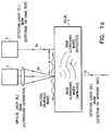
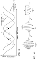
- Figs. 1a-1d there are four types of waves which can propagate in a target, such as a solid 1, namely longitudinal, shear, Rayleigh or surface, and Lamb waves (shown in Fig. 10a).
- the longitudinal and/or shear waves travel only through the bulk of the solid, with the longitudinal waves having a velocity that is approximately twice that of the shear waves.
- the Rayleigh waves travel only on the surface of the solid with velocities slightly less than that of the shear waves.
- the Lamb waves are supported by and propagate through very thin solids, and may be used to measure the thickness of the solid 1.
- Longitudinal bulk waves and shear bulk waves have been extensively used for the detection of flaws, measurements of elastic properties of solids, and for the monitoring of phase transitions, such as occurs when a molten metal solidifies. It is also well-known to measure the temperature of the solid 1, as the temperature effects the velocity of the waves within the solid.
- a number of different types of transducers have been employed to generate elastic or ultrasound wave energy in solids.
- a laser e.g., impulse laser 2
- a detection laser 3 such as is found in an optical interferometer, to detect a movement of the surface of the solid 1 in response to the propagating ultrasound waves.
- the velocity of the wave in the solid 1 can be determined; so long as the distance d is known between the spot where the impulse laser beam 2a impinges and where the detection laser beam 3a impinges.
- the determined velocity, or 'time of flight' may then be correlated with some property of interest of the solid, such as the structure of the solid or the temperature of the solid.
- some property of interest of the solid such as the structure of the solid or the temperature of the solid.
- the impulse laser beam 2a and the detection laser beam 3a are directed to opposite sides of the solid, as in Fig. 1d, it is possible to measure the thickness of the solid. The thickness can also be measured, with the impulse and detection laser beams impinging on the same side, if the solid is thin enough to support a Lamb wave.
- U.S. Patents in this and related technical areas include the following: U.S. Patent 3,601,490, issued 8/24/71 to K. Erickson and entitled “Laser Interferometer”; U.S. Patent 3,694,088, issued 9/26/72 to J. Gallagher et al. and entitled “Wavefront Measurement”; and U.S. Patent 4,633,715, issued 1/6/87 to J. Monchalin and entitled "Laser Heterodyne Interferometric Method and System for Measuring Ultrasonic Displacements".
- One intended operating environment for this type of system is in a metals fabrication and/or treating facility.
- a metals fabrication and/or treating facility As can be appreciated, and because of the ambient heat, vibration and airborne particulate matter that is typically found in this type of environment, severe demands and operating stresses are placed on the interferometer and its associated detection laser and optical elements.
- Another important consideration is the cost of the system, as an industrial application may require the use of a number of materials analysis systems. That is, it is desirable to provide a rugged, compact and low cost system without compromising measurement accuracy and repeatability.
- This invention provides an interferometric-based laser ultrasonics materials analysis system that is improved over known types of systems. This is achieved through a novel combination of laser beam shaping and pointing techniques, the use of a low cost, rugged, and compact diode laser assembly as a detection laser, various techniques to optimize the system for use with the diode laser-based detection laser, and the use of signal processing techniques that compensate for inherent instabilities and short-term drift in the diode laser. In addition, matched filter processing techniques are disclosed for processing interferometrically-obtained data points from a target being analyzed.
- an impulse source such as an impulse laser
- a plurality of data points so obtained are subsequently processed, such as by the matched filter technique, to determine a property of interest of the target.
- the property of interest may be, by example, the temperature of the target or the metallurgical status of the target.
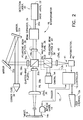
- Fig. 2 is a block diagram of a presently preferred embodiment of a laser ultrasonics materials analysis system 10 that is constructed and operated in accordance with this invention.
- the system 10 generally operates by launching an elastic wave within a target, sensing a surface displacement of the target due to the elastic wave, and then correlating the sensed displacement with a value of a property or properties of interest.
- an elastic wave is intended to also encompass an acoustic wave.
- a target may be a solid, a semi-solid, or a liquid.
- a system controller 12 such as an embedded microprocessor or an externally connected computer or workstation, includes a user interface 12a that includes, by example, a touchscreen and/or a conventional keyboard and/or a pointing device (e.g., mouse) in combination with a graphical display device through which a user is enabled to interact and direct the operation of the system 10.
- An impulse laser 14 is controlled by the controller 14 to provide an impulse beam 14a to the surface of an object, hereafter referred to as a target 16 (the target forms no part of the system 10, and is shown only for completeness).
- the impulse beam 14a causes a localized heating of the target 16 and launches an elastic wave within the target as described previously.
- a displacement of the surface of the target 16 due to the elastic wave is detected by a polarizing interferometer 18 that is constructed and operated in accordance with this invention.
- the interferometer 18 includes a detection laser 20 which, in the presently preferred embodiment of the polarizing interferometer 18, includes a diode laser 22.
- the diode laser 22 provides high power (>100mW) along with the combined characteristics of small dimensions, low cost (relative to more conventional detection lasers such as the He-Ne), and a long coherence length (i.e., narrow bandwidth).
- Commercially available diode laser systems can provide >100mW of power with bandwidths that range from 10 MHz to less than 10KHz.
- the selection of a particular diode laser for use in the system 10 is a function of the required power, coherence length, wavelength, system compactness, and cost.
- the detection laser 20 is a conventional Faraday rotator (not shown) to prevent any reflected laser light that returns from the target 16 from effecting the performance of the diode laser 22.
- a conventional Faraday rotator (not shown) to prevent any reflected laser light that returns from the target 16 from effecting the performance of the diode laser 22.
- the output of the detection laser 20 assembly is a source beam 20a.
- Fig. 16 for illustrating a novel and preferred diode laser assembly 21. It is first pointed out that some diode lasers have been conventionally stabilized by an external cavity formed by a grating mounted in a Littrow configuration. The first order reflection off the grating provides feedback into the laser cavity and the zero order reflection provides the output coupling.
- the diode laser assembly 21 of Fig. 16 employs a novel technique for mounting and aligning a grating which is very stable (thermally and mechanically), and at the same time inexpensive to manufacture and simple to construct.
- a laser diode 21a and a collimating lens 21b are mounted on an end of a support structure (e.g., a tube 21c made from stainless steel or some other suitable rigid material).
- a support structure e.g., a tube 21c made from stainless steel or some other suitable rigid material.
- the tube 21c has a length of six inches and a diameter of two inches.
- the diode laser 21a has an anti-reflection (AR) coating on its output facet to eliminate facet modes which would conflict with external modes established by a grating 21d.
- the grating 21d is mounted on a fixed angle pedestal 21e, the angle ( ⁇ 1) of which is selected to provide a desired operating wavelength of the laser diode 21a.
- the accuracy of the machined angle required for tuning the laser diode emission to ⁇ 1 nm is approximately ⁇ 0.8 degrees, a value well within simple machining tolerances.
- the angle of the tuning axis (in the plane of the drawing) is not critical and, thus, no adjustment mechanism is necessary (although one may be provided if desired).
- the angle out of plane (the alignment axis AA) cannot be readily machined to sufficient accuracy.
- this angle is adjusted by rotating a wedge 21f about the axis approximately parallel to the laser beam.
- the wedge 21f is positioned between the diode laser 21a and the grating 21d and functions to change the angle of the laser beam.
- the wedge 21f is supported by a rotation stage mount 21g.
- the angle ⁇ 2 is the Littrow angle associated with the grating 21d, and the optical cavity external to the diode laser 21a extends generally to the face of the grating 21d.
- the wedge 21f is preferably anti-reflection coated to minimize cavity losses, and is also tilted with respect to the beam axis so that reflections off either wedge surface will not go back into the laser diode 21a.
- the source beam 20a is provided to a beam expander 24.
- the characteristics of the beam expander 24 directly impact the light collecting power of the sensor system described below. In general, the larger the beam diameter, the larger the return speckle size, and thus the greater is the fraction of the total returned power that is available to interference signal generation.
- the beam expander 24 can be placed either before or after a polarizing beam splitter 28 that is described below. Placing the beam expander 24 after the beam splitter 28 has the advantage that the interferometer optics can be made smaller and also independent of the expansion ratio of the beam expander 24. However, placing the beam expander 24 at this position requires that the detection or probe beam (PB) 28b pass through the beam expander 24 twice. As a result, the quality (cost) and alignment of the beam expander 24 becomes important to the overall operation of the system 10. As such, and although it is preferred to place the beam expander 24 before the polarizing beam splitter 28, as illustrated in Fig. 2, the teaching of this invention is not so limited.
- the expanded source beam 24a next encounters a halfwave plate 26 that is located before the polarizing beam splitter 28.
- the halfwave plate 26 provides a mechanism for setting a desired ratio for a reference beam (RB 28a) to probe beam (PB 28b) intensity. Varying the rotation angle of the halfwave plate 26 rotates the polarization of the laser beam and, in combination with the operation of the polarizing beam splitter 28 that is described next, thereby controls the fraction of the beam going into the PB 28b and into the RB 28a of the interferometer 18.
- the halfwave plate 26 may be coupled to a mechanism, such as a motor, for imparting a rotary motion to the halfwave plate 26.
- the controller 12 automatically monitors the signal returned from the target 16 and controllably rotates the halfwave plate 26, via signal line 12b, so as to optimize the relative intensities of the reference and probe beams.
- this function can be performed by user who monitors a graphical display provided by a camera 44 (described below).
- the rotated beam 26a that passes through the halfwave plate 26 is split into the RB 28a and PB 28b by the polarizing beam splitter 28, with the RB 28a and PB 28b having relative intensities set by the rotation imparted by the halfwave plate 26.
- the polarizing beam splitter 28 After the reference and probe beams 28a and 28b leave the polarizing beam splitter 28 each passes through an associated 1/4 wave retardation plate 30a and 30b, respectively. Plates 30a and 30b are aligned so that both of the RB 28a and PB 28b are circularly polarized.
- the path length of the RB 28a is adjusted to reduce the noise in the signal that is detected from a combined beam (CB) 28c.
- the degree to which the lengths of the probe leg and the reference leg are matched is a function of the bandwidth of the diode laser 22, the fraction of the signal noise that is attributed to any frequency jitter of the diode laser 22, and the impact of the length of the reference leg on the overall compactness of the interferometer 18.
- RB 28a leg Included within the RB 28a leg are a plurality of folding mirrors 32a and 32b and a corner cube reflector 34. It is important to the operation of the interferometer 18 that the reference leg return beam be at the same angle (opposite direction) as the outgoing reference beam. This important goal is achieved in a simple, compact, and inexpensive manner using the corner cube 34. In contrast, a simple mirror would require careful and precise adjustment, and very high quality mounts all along the reference path to maintain the alignment. In the presently preferred embodiment of this invention these requirements are eliminated by the use of the corner cube 34 (preferably gold coated and hollow) which terminates the reference beam path leg while preserving the polarization characteristics of the RB 28a.
- the corner cube 34 preferably gold coated and hollow
- the PB 28b is focussed to a point on the target 16 using a lens 36 that has a focal length equal to the distance to the target 16. That portion of the PB 28b that reflects from the surface of the target 16 is subsequently collimated by the lens 36 as it travels back into the interferometer 18.
- the same prism (the polarizing beam splitter 28) that is used to split the polarized beam 26a into the RB 28a and the PB 28b is also is used to recombine the RB 28a and the returned (reflected) portion of the PB 28b into a combined beam (CB) 28c.
- the RB 28a and the PB 28b are circularly polarized, and must pass back through the 1/4 wave plates 30a and 30b, respectively, they are again linearly polarized, but at the opposite orientation than their original linear polarizations. Because of this, the CB 28c does not go back toward the diode laser 22, but instead is directed into a signal detection portion of the interferometer 18.
- a polarizing prism or beam splitter 38 oriented at 45° is used to select a projection of the polarization axis of each of the RB 28a and the PB 28b along a common axis.
- Fig. 5 illustrates the use of two photodetectors (PD-1 and PD-2) for detecting two combined beams.
- a combined beam focussing lens 40 is used to focus the CB(s) 28c onto a radiation sensitive surface of one or more photodetectors 42.
- the lens 38 in combination with an aperture 41, can also be used to spatially block out light other than that of the combined beams from impinging on the photodetector 42.
- the photodetector 42 may be provided in a number of suitable forms, depending on performance characteristics. Both conventional photomultiplier tubes and hybrid photodiode/amplifiers are suitable embodiments for detecting the light and dark pattern that results from the interference of the RB 28a and the returned portion of the PB 28b within the CB 28c. The output of the detector 42 is provided to the controller 12 for signal processing in the manner described below.
- An optional camera 44 is primarily used as a diagnostic tool, i.e., the camera 44 useful for optimizing the detected signal when an operator is setting up and controlling the system 10.
- the camera 44 which may be a conventional CCD device that provides an output to a display monitor of the user interface 12a, provides visual feedback to the operator for best signal return, which implies a best pointing angle to the target 16.
- an automatic beam steering system performs this function without operator intervention.
- the camera 44 may also be used for alignment of the signal and reference beams.
- the camera 44 can also be employed to determine the relative intensity of the reference and signal beams and, based on the indicated intensities, the operator is enabled to rotate the halfwave plate 26 to achieve an optimum intensity distribution for optimum fringe contrast.
- a second photodiode 42 can be installed in its place.
- the use of a second photodiode 42 enables a square and add signal processing technique to be used as described in U.S. Patent 5,286,313, which has been incorporated by reference herein.
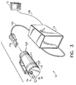
- Fig. 3 depicts an elevational view of the system 10, and shows a bulkhead-mounted optical head 11, a base unit 13, and the controller 12.
- the optical head 11 is constructed to have a slide-in unit 11a that contains the impulse laser 14, the interferometer 18, and all associated electronics and controls.
- the optical head 11 includes a jacket 11b through which a cooling fluid (e.g., water) is flowed during the operation of the system 10.
- the slide-in unit 11a is thermally coupled to the water jacket 11b when inserted into the head 11, which thereby functions to remove the heat that is generated by the operation of the lasers and associated electronics, although a primary function of the water jacket 11b is to remove the external heat load during high temperature operation.
- the base unit 13 contains all required power supplies and provides, via cabling 13a and 13b, an interface to the controller 12.
- the optical head is instead tripod-mounted and may not be water-cooled.
- Fig. 4 is a top view of an exemplary embodiment of a slide-in unit 11a that is suitable for use in the above-mentioned tripod-mounted embodiment of the invention.
- a baseplate 50 provides a rigid support for mounting all of the required lasers and optical components.
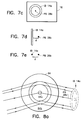
- the impulse laser 14 has its output connected to a variable beam attenuator 50 and to a beam-shaping negative axicon 52a (Fig. 7a).
- the negative axicon 52a provides, in accordance with an aspect of this invention, a ring-shaped annular impulse beam 14a for impinging on the target 16.
- a waxicon 52b (Figs. 7b and 7b') is employed instead.
- One difference between these embodiments is that the negative axicon 52a works in transmission, while the waxicon 52b works in reflection.
- a second difference is that the use of the waxicon shortens the beam path.
- the shaped impulse beam is folded by mirrors 54, 56, 58 and combiner 60 before being provided to rotatably mounted beam steering mirrors 62 and 64, connected to a motor 64a, which direct the impulse beam 14a towards the target 16 at a controlled and optimum angle.
- This aspect of the invention is described in detail below with regard to Figs. 8a and 8b.
- the detection laser 20 is provided as a modular unit that includes the laser diode 22 and an externally mounted resonant cavity for narrowing the bandwidth of the laser diode 22. It is also preferred to use an antireflection (AR) coating to eliminate any internal modes of the laser diode. It is further preferred to employ a current control technique that uses a photodiode detector to sense any instability in the output of the laser diode 22 and, in response, that perturbs the laser diode current by some predetermined amount (e.g., 0.1% - 1%). The laser diode 22 is operated as a continuous duty device. That is, and as will be made apparent below, an interference signal from the target 16 is available whether or not the impulse laser 14 is being triggered. A preferred embodiment of a diode laser assembly is illustrated in Fig. 16 and was described previously.
- the output of the laser diode 22 is provided via mirrors 66 and 68 to the aforementioned Faraday rotator 70 and then to the halfwave plate 26 (beam polarization rotator).
- the beam polarization rotator 26 is positioned in front of the beam expander telescope 24. Coupled to the output of the beam expander telescope 24 is the polarizing beam splitter 28.
- the output of the beam splitter 28 impinges on a mirror 72 from which it is directed to an optical path wherein the beam is folded a number of times between a mirror 74 and reflectors 76 and 78.
- the probe beam 28b is output along with the impulse beam 14a towards the target 16 via the beam steering mirrors 62 and 64.
- the folding of the probe beam between mirrors 74, 76 and 78 is an aspect of this invention related to the use of the diode laser as the detection laser 20.
- the coherence length of a typical diode laser is in the range of 30 meters to 40 meters.
- This path matching is used in combination with the grating 21d (Fig. 16), the Faraday rotator, the beam expanding telescope 24, and the focussing lens 36 (to provide at least one bright speckle), in order to optimize the interferometer 18 for use with a diode laser as the detection laser.
- the components 80 and 82 are shutters. Also shown is the camera 44, the photodetector 42 and, in dashed outline 84, a support electronics package. As can be appreciated, the impulse laser system and the interferometer 18 are provided in a small area and the beams are tightly folded to minimize the required mounting area.
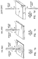
- the impulse beam 14a with a shape that corresponds to a ring, a line, or a point.
- the ring-shape is preferred (using the negative axicon 52a or the waxicon 52b), but there are many applications where the other shapes become important.
- the probe beam 28b is preferably tightly focussed to a diffraction limited spot.
- the probe beam 28b is located at the center of the ring (Fig. 7c), and the time of flight (TOF) of the elastic wave launched by the IB 14a is measured across the radius of the ring.
- the probe beam 28b is separated by a fixed distance d, for example 0.5" to 1", away from the impulse beam 14a (see Figs. 7d and 7e, respectively), and the TOF is measured across the distance d.
- the conical surface is concave.
- the same impulse laser ring-shape on the target can be obtained with a convex surface (positive) axicon, but immediately after the axicon there will be a caustic focus which creates a line-shaped zone of intense laser fluence which can cause damage to optics placed in its path.
- the length of this zone extending from the axicon is a function of the angle of the axicon and the diameter of the impulse beam, and can extend several inches.
- the concave surface axicon there is no limit on how close subsequent optics can be placed. As such, the use of the concave surface axicon is preferred, although the teaching of this invention is not limited to only this configuration.
- a problem that arises during the use of an axicon is that the impulse beam 14a ring diverges and the diameter of the ring on the target will vary as a function of distance to the target. Such a situation is unacceptable as the system 10 would not operate correctly with moving or vibrating targets because the target distance, and thus the diameter of the IB 14a ring, will change continuously. In this case the time of arrival of the elastic waves at the location of the PB 28b will also be continually changing, and there would be no way to distinguish between a change in the arrival time due to the target motion (a change in ring diameter) or that due to a change in a property of the target (a change in elastic wave arrival time).
- This problem is overcome in the system 10 by ensuring that the ring-shaped IB 14a exiting the head 11 is of constant diameter and is not expanding (diverging) or converging. This is achieved by causing the impulse beam 14a to travel a predetermined distance within the head 11 before it is focused onto the target 16.
- the predetermined distance is approximately equal to the distance of the head 11 to the target 16, and is achieved through the use of adjustable path length folding optics represented by the components 54, 56, 58, 60 and 62 of Fig. 4.
- the optical properties of the reflective waxicon 52b of Figs. 7b and 7b' also solve this problem of impulse beam divergence or convergence and provide an impulse beam ring of constant diameter, while reducing or eliminating the requirement to provide the extended light path inside the head 11. As a result, the use of the waxicon 52b is desirable to reduce the volume of the head 11.
- the waxicon 52b is comprised of a substrate 53, such as aluminum, having a diamond machined reflective surface 53b ( ⁇ /4).
- a suitable diameter is three inches, and a suitable maximum thickness (TH) is one inch.
- a suitable value for angle ⁇ 1 is 45°, while a suitable value for angle ⁇ 2 is approximately 45.3°.
- an annular output beam 53d is generated with a diameter (BD) of approximately two inches.
- Other materials, dimensions and angles may be employed, depending on the requirements of a particular application.
- the impulse beam 14a and the probe beam 28b may be located on the same side of the target 16 or, with additional reflectors and path optics, on opposite sides of the target 16.
- the stability of the probe beam 28b is determined by the duration of a time interval during which the wavelength of the detection laser 20 can shift by no more than a predetermined maximum quantity or number of wave numbers.
- the maximum quantity or number of wave numbers corresponds to a frequency in the range of 10 kHz to 100 kHz.
- this stability requirement is at or beyond the limit of the capabilities of currently available laser diode systems, or of most if not all types of laser systems that would be required to operate in the adverse environments within which the system 10 may be required to operate.
- a combination of mirrors 62 and 64 is employed to steer both beams (it being remembered that the impulse beam 14a may be a ring with the PB 28b at its center).
- the beam steering mirrors (actually the combination of the mirrors 62 and 64) have a reflective "patch" in their center, i.e., a small area 64a that is coated with a metal (e.g., gold) to reflect the PB 28b (which is in the infrared spectrum), while the remainder of the surface of the mirror 64 has a conventional dielectric coating 64b to reflect the impulse beam 14a, which may be in the green portion of the visible spectrum. Since the energy flux of the impulse beam 14a is quite high, providing a dielectric coating is desirable to avoid optical damage.
- a metal e.g., gold
- the PB 28b must maintain its polarization during reflections, and hence the metallic (gold) patch 64a is preferred over a conventional dielectric-coated mirror, which will induce a change in polarization.
- the use of specific reflection materials and dielectric coatings can be generalized to whatever combination is appropriate for the wavelengths that are being used.
- the choice of the IB 14a and the PB 28b wavelengths is not random, and there are several criterion involved in a specific choice of wavelengths.
- the laser light interaction with the target surface is wavelength-dependent, and it has been found that metal targets respond best to green or ultraviolet (UV) wavelengths for the IB 14a.
- UV ultraviolet
- many composite materials give optimum results with IB 14a wavelengths in the far infrared.
- the sensitivity of the photodetector 42 is a function of the wavelength of the CB 28c and, hence, the emission wavelength of the laser diode 22.
- the system 10 is observing a target with a very diffuse reflectivity (near Lambertian), it is not critical that the viewing axis is normal to the surface. In fact, the intensity is still 50% of its peak value when the viewing axis is 45 degrees off normal. There are, however, surfaces such as those associated with non-polished metallic materials where the intensity drops of much faster as a function of angle. The intensity may drop to 10% of its peak value in a range of 1 to 10 degrees. For these situations it is desirable to provide an automatic system which adjusts the beam angle (preferably both impulse and probe) to stay near normal to the surface. This is important for applications such as viewing a moving strip in a metals processing plant where a common twisting motion of the strip can change the angle by as much as ⁇ 10 degrees.
- the output of the alignment laser 65a passes through a lens 65b which is selected so that the beam coming out of the instrument illuminates a spot on the target which, relative to the position of the instrument window, subtends an angle larger than the possible angular variation of the target 16.
- the alignment beam from alignment laser 65a is combined with the PB 28b from detection laser 22 using a dichroic beam splitter 65d.
- the dichroic beam splitter 65d reflects the alignment laser beam AB but transmits the PB 28b.
- Alignment laser light returning from the target 16 is imaged onto a position sensitive detector 65e with an imaging lens 65f.
- One suitable embodiment for the detector 65e is a well known silicon quadrature detector.
- the imaging lens 65f is selected to have the beam spot on the target imaged to about the same size as the detector 65e.
- a 50/50 beam splitter 65c provides a simple method to both reflect out the alignment laser, and pass the returning beam (returning on the same axis AB) to the imaging lens 64f and the detector 65e. Although half the intensity is lost on the outgoing path and half on the incoming path, this technique is simpler and less expensive than using a polarizing beam splitter and quarter wave plate to eliminate these losses.
- target reflectivities are low, or available alignment laser powers are too low, this more involved technique can be used.
- the intensity distribution on the detector 65e is very similar to that of the alignment laser-produced spot on the target 16. If the reflectivity drops of quickly with angle there will be a bright spot within the image on the detector 65e. If the viewing angle is normal to the surface of the target 16, this bright spot will be centered within the image on the detector 65e.
- the intensity information from the detector 65e is provided to closed loop control circuitry (not shown) which drives xy tilt mechanisms 65g on steering mirror 64 to bring the bright spot to the center of the image on the detector 65e.
- the probe and impulse beams 28b and 28a are maintained normal to the surface of the target 16, which is the desired result.
- Some materials such as rolled aluminum, have different reflectivity angular distributions for the axis along a strip relative to the axis perpendicular to the strip. This may necessitate greater sensitivity along one axis compared to another. This can be accomplished by using an elliptical spot on the target 16 (minor axis in the direction of greater required sensitivity) and providing the lens 65f as one or more cylindrical lenses to image the orthogonal axis of the ellipse separately on to the detector 65e. The cylindrical lenses function to create a circular spot on the detector 65e.
- Fig. 5 shows the transfer functions for two photodetectors 42 that are 90° apart in phase, although it should be realized the system 10 may operate with one, two, or even more photodetectors 42. What should be evident from this transfer function is that the most sensitive, and hence the most desirable and optimum points of operation are at the maximum slopes, i.e., points E, C, F, D.
- An interferometer may use vibrating mirrors or other moving parts to adjust or dither the reference leg of the interferometer so as to force the system to operate at such points.
- this approach may not be desirable for all applications in that it adds to the overall complexity and cost of the system.
- the system 10 operates at these optimum points, without the use of moving optical components, by an algorithmic technique that results in the triggering of the impulse laser 14 only at times when the signal received from the photodetector(s) 42 is optimum.
- Fig. 6 shows a typical signal received from a target 16 (moving in this case, but static targets have a similar response). As shown, there are "bursts" of sinusoidal signals designated as A, D, and C, interspersed with regions B of little or no sensitivity (flat line). The bursts occur, typically, over a time (t) of two to four milliseconds.
- the regions A, B and C represent 'poor' signal regions, while the region D represents a 'good' signal region, i.e., low frequency target motion and a high signal amplitude.
- the poor region A exhibits a high signal amplitude, but also has a high frequency of target motion.
- the existence of the region A is usually due to target motion and, in most cases, regular environmental vibrations that cause oscillations of low frequency. It is important to note that these oscillations are not of the same frequency as the environmental vibrations, but instead represent the number of wavelengths per unit time received by the interferometer 18. For example, a low frequency, but very large amplitude, external vibration can cause the target 16 to move by many millions of wavelengths in a very short time. On the other hand, the same condition can be caused by a high frequency, but low amplitude vibration. If the frequency of these wavelengths reaches the useful data range (for example, 300 kHz to 2 MHz), then no subsequent filtering action can separate the desired signal from the external vibrations. The situation may be referred to as "frequency poisoning".
- the existence of the regions B of Fig. 6 can be attributed to one or more of the following: (a) no return light, hence no interference, which can be caused by receiving a dark speckle from the target 16 (light and dark speckles are randomly distributed); and (b) no interference due to a lack of diode laser 22 coherence, which can be caused by instability in the laser operation or signal/reference leg path differences being larger than the coherence length of the diode laser 22.
- the region C exhibits a low frequency of target motion, but also has a low signal amplitude. This can be due to a lack of contrast in the interference fringes or by an insufficient amount of returned light.
- the system 10 operates with an impulse laser 14 "trigger on demand” (TOD) technique that triggers the impulse laser 14, and hence collects data, only during a period of reception of a "good” signal (i.e., region D of Fig. 6).
- TOD trigger on demand
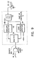
- the controller 12 includes a bandpass filter 90 that is coupled to the photodiode (PD) 42.
- the desirable signals When operating in the Rayleigh mode the desirable signals are generally in the range of approximately 1-5 MHz, while when operating in the Lamb mode the desirable signals are generally in the range of approximately 100 kHz to 1 MHz.
- the output of the filter 90 is connected to an envelope detector 92 and to a zero crossing detector 94.
- the envelope detector 92 determines the amplitude of the bursts received from the photodiode 42, while the zero crossing detector 94 detects the zero crossings and, hence, the frequency component of the sinusoidal bursts.
- An analyzer 96 monitors the output of the envelope detector 92 and the output of the zero crossing detector 94 to determine a condition wherein both the burst amplitude and frequency indicate that a 'good' burst is occurring. The occurrence of such a good burst indicates a lack of all or most of the undesirable conditions described in conjunction with the regions A, B and C or Fig. 6 (e.g., loss of laser diode coherence, unacceptable target motion, the reception of a dark speckle, etc.). The analyzer 96 then triggers the impulse laser 14 to initiate a measurement during the remaining period of the good burst. This trigger point (TP) is indicated in the region D of Fig. 6.
- the timing of the trigger may also be selected so that an expected elastic wave detection will occur at or near an optimum point on the sinusoidal signal.
- the TP occurs at a point corresponding to point A in Fig. 5, which results in the launched elastic wave passing under the probe beam 28b at or about the optimum measurement point C on the sinusoid.
- any latencies in the operation of the impulse laser 14 are also considered, and the initiation of the trigger 96a is adjusted accordingly. Typical latencies are in the range of 100 ⁇ sec to 200 ⁇ sec.
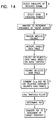
- Fig. 9 may be executed wholly or partially by a suitably programmed processing device.
- a method of this invention there are performed the steps of (A) detecting the envelope of the received signal to determine the amplitude of the sinusoidal oscillations; (B) detecting zero crossing points of the sinusoidal oscillations to identify the frequency of the burst; (C) analyzing the detected amplitude and the detected frequency to determine an occurrence of a good burst; and (D) triggering the impulse laser 14 at an appropriate time in order to collect data at the maximum slope operating points of the polarizing interferometer 18, i.e., points E, C, F, or D of Fig. 5.
- the signal processing of the received signal proceeds as follows: (E) acquiring a trace of signal vs. time; (F) accepting or rejecting the data based on criteria of allowable signal noise; (G) squaring the data; (H) accumulating similar data traces and combining them by adding the data, or by using techniques such as weighted averaging; (I) using a 'matched filter' to extract a feature of interest from the processed signal; (J) calculating the TOF from the 'matched filter'; and (K) converting the TOF to useful properties of the material (such as temperature, metallurgical status, etc.) by using predetermined calibration curves.
- the Rayleigh regime i.e., non-dispersive surface wave mode
- the S o and A o Lamb modes are detected and are employed in combination to obtain the temperature of the target 1. That is, equations with two unknowns (thickness and temperature) are solved based on the S o and A o velocities which are detected in response to the application of the impulse beam 14a.
- One particularly useful application is in detecting the temperature of a thin substrate, for example a silicon substrate having a thickness in the range of approximately 200 to 400 micrometers. An embodiment of this application will be described below with reference to Fig. 12.
- a matched filter library 100 is employed in conjunction with a matched filter processor 102 to determine the thickness of a substrate.
- a plurality of wave templates or shapes 100a are digitized and stored during a training mode of operation using samples of predetermined thickness (100b).
- the stored shapes are each based on a plurality of measurements taken on a single sample.
- the measurements are preferably filtered and otherwise processed to eliminate noise and other artifacts of the measurement process.
- Each stored wave shape 100a thus represents an average of the plurality of measurements.
- the training mode is indicated schematically by the switch S1 being in a closed position.
- the PD 42 output signal is applied to the matched filter processor 102 as an input signal.
- Individual ones of the stored shapes 100a are compared to the input signal to determine a best match through an autocorrelation technique (indicated by the arrow).
- the best match shape 100a is then correlated with its associated thickness 100b. Having determined the thickness of the sample, the temperature can be determined.
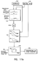
- Fig. 11b illustrates a second signal processing embodiment, specifically a calibration technique for velocity measurements.
- this is a method to convert the TOF measurements to velocity and then to, by example, temperature.
- This technique is especially applicable to thin targets, where Lamb modes are used and dispersive behavior is observed.
- temperature is used as an example, the method can be generalized for other material properties.
- the TOF of the elastic wave is illustrated, this embodiment may be generalized to determine a time varying characteristic (e.g., frequency, phase, etc.) of the elastic wave.
- the inputs to this signal processing embodiment may be manually or automatically generated.
- the thickness of the target can be automatically inferred by the method described in Fig. 11a, or may be manually inserted from the user interface 12a.
- the inputs are the target thickness 104 and material type 105.
- the material type 105 may be, by example, the identification of an alloy.
- the separation distance (SD) between the impulse beam 14a and the probe beam 28b may be provided as a constant.
- a library of "matched filters" 106 and a library of calibration curves 107.
- the library of calibration curves 107 may represent, by example, velocity vs. temperature (see, for example, Fig. 15) or, more generally, one or more ultrasonic pulse or elastic wave characteristics vs. material property (e.g., temperature).
- the thickness and material type inputs 104 and 105 are used to select one of the stored matched filters from library 106 and a calibration curve from the library 107. Having selected a corresponding matched filter from the library 106, the processed data waveform is then compared with the selected matched filter until a best match is obtained. This is a correlation operation that yields the TOF 106a. The TOF 106a is then converted to the velocity of the elastic wave based on the SD.
- the temperature or some other material property is determined in block 108 and is output as a result 109.
- FIG. 12 An application of the Lamb mode processing technique of this invention is illustrated in Fig. 12.
- This figure generally shows a rapid thermal processing (RTP) system 110 which is used for the thermal processing of a silicon wafer 112.
- RTP rapid thermal processing
- a heater module 114 surrounds a portion of a process chamber 116 which is covered by a layer of thermal insulation 118.
- a lower transfer chamber 120 enables the wafer 112 to be loaded into and extracted from the process chamber 116.
- an elevator assembly 122 is used to raise and lower the wafer 112 within the process chamber 116.
- a very rapid heating e.g., 50-100°/sec
- a pyrometer head 132 is connected via an optical fiber 134 to a pyrometer 136 for measuring, by emissivity, the temperature within the process chamber 116.
- the pyrometer 136 is interfaced to the process controller 124 to close the temperature control loop.
- the RTP system further includes the laser ultrasonics materials analysis system 10 of this invention.
- the head 11 is disposed so as to direct the impulse beam 14a and the probe beam 28b onto a surface of the wafer 112 during the thermal processing of the wafer.
- the Lamb mode of operation (Fig. 11b) is preferably utilized to determine the wafer temperature. Due to the crystalline nature of the silicon wafer 112 the S o Lamb mode is more apparent because there is less background noise than would be found in, for example, a metal substrate of the same dimensions. This enables temperature measurements of the wafer 112 with an accuracy equal to or less than ⁇ 5°F. This temperature measurement occurs without using the emissivity of the silicon wafer, which would be difficult to accurately measure within the high ambient temperature of the process chamber 116.
- Fig. 13 shows another exemplary application of the system 10.
- the system 10 is used to monitor the surface temperature of boiler tubes 140 within a furnace 142. Such an arrangement is often found within a petrochemical refinery.
- One or more view ports 144 enable optical access to the boiler tubes 140.
- the IB 14a and PB 28b are directed onto the surface of a boiler tube wall 140a. If a deposit build up (shown generally as 140b) occurs on the inner surface of the boiler tube wall 140a, a hot spot is created on the outer surface. The presence of such a hot spot is undesirable in that it can eventually lead to metal fatigue and the failure of the affected boiler tube 140. Since the boiler tubes normally carry a pressurized heated volatile fluid, such a failure can be catastrophic.
- the use of the system 10 enables a remote (non-contact) and very accurate reading of surface temperature along the boiler tube outer walls and thus enables a detection of surface hot spots before metal failure occurs.
- An exemplary, but certainly not exhaustive list of other applications that may benefit from the remote, contactless temperature measurement system of this invention include the heat treating industry (measurement of internal and surface temperature of steel, aluminum, etc.); the carburizing industry (measurement and control of carburization depth and surface hardness); phase change processing (as shown in Fig. 15, the detection of onset and completion of phase changes during steel processing); and nondestructive inspection (detection of internal flaws, cracks, and voids in structures). In the flaw detection application additional signal peaks are observed which arise from internal flaws within a structure (such as bridge support) under test.
- Another application of interest is the process control of paper, i.e. mechanical strength, water content, etc.
- one technique is to first detect the arrival of the wave (peak detection) and then from the Time-Of-Flight (TOF) calculate the velocity by knowing the distance or the path length.
- the determined elastic wave velocity correlates with many properties of the target, such as temperature, metallurgical status, etc.
- the velocity measurement is not the only suitable method for analyzing the signal.
- any time varying characteristic of the received elastic wave may be used to monitor various material properties, such as carbon content, case depth, grain size, etc.
- Exemplary time varying characteristics include the frequency of the received elastic wave, the phase of the received elastic wave, and an amplitude modulation of the envelope of the received elastic wave.
- Methods such as Fast Fourier Transformations, Wavelets, etc. are used in the system 10 to measure the time varying content, such as frequency characteristics, of the received elastic wave so as to correlate the measured time varying content with one or more material properties of interest.
- a thickness test it is within the scope of this invention to eliminate a thickness test altogether when determining a material's properties. More particularly, when thick targets are being investigated (e.g., thicker than 0.125") and bulk waves are being used, then there is a need for prior sided (reflected waves from opposite side) and double sided (one pass through target) configurations. In both of these cases the travel distance of the elastic wave needs to be known in order to calculate the velocity from the TOF measurements.
- a method for determining the travel distance is to generate an elastic wave in the target and to then detect the arrival of both Longitudinal (L) and Shear (S) waves.
- L Longitudinal
- S Shear
- the latter travel with almost half the speed of the former. Therefore these waves arrive at different points in time and can thus be detected separately.
- the ratio of the determined L and S TOFs are used to infer the ratio of the L and S velocities (Block B).
- the travel path drops out of this calculation, since it is the same for both waves. Therefore, instead of correlating the velocity of each wave with the target properties, the ratio of the L and S velocities is correlated with a target property of interest (Block C), thereby avoiding any thickness uncertainty.
Landscapes
- Physics & Mathematics (AREA)
- General Physics & Mathematics (AREA)
- Health & Medical Sciences (AREA)
- Life Sciences & Earth Sciences (AREA)
- Chemical & Material Sciences (AREA)
- Analytical Chemistry (AREA)
- Biochemistry (AREA)
- General Health & Medical Sciences (AREA)
- Immunology (AREA)
- Pathology (AREA)
- Acoustics & Sound (AREA)
- Optics & Photonics (AREA)
- Engineering & Computer Science (AREA)
- Signal Processing (AREA)
- Condensed Matter Physics & Semiconductors (AREA)
- Electromagnetism (AREA)
- Length Measuring Devices By Optical Means (AREA)
- Instruments For Measurement Of Length By Optical Means (AREA)
- Investigating Or Analyzing Materials By The Use Of Ultrasonic Waves (AREA)
- Investigating Or Analysing Materials By Optical Means (AREA)
Applications Claiming Priority (2)
| Application Number | Priority Date | Filing Date | Title |
|---|---|---|---|
| US30837294A | 1994-09-19 | 1994-09-19 | |
| US308372 | 1994-09-19 |
Publications (2)
| Publication Number | Publication Date |
|---|---|
| EP0702230A2 true EP0702230A2 (de) | 1996-03-20 |
| EP0702230A3 EP0702230A3 (de) | 1999-02-24 |
Family
ID=23193730
Family Applications (1)
| Application Number | Title | Priority Date | Filing Date |
|---|---|---|---|
| EP95114555A Withdrawn EP0702230A3 (de) | 1994-09-19 | 1995-09-15 | Laser-System und Verfahren zum Untersuchen von Materialien mittels Ultraschall |
Country Status (3)
| Country | Link |
|---|---|
| US (6) | US5604592A (de) |
| EP (1) | EP0702230A3 (de) |
| JP (1) | JPH08184581A (de) |
Cited By (7)
| Publication number | Priority date | Publication date | Assignee | Title |
|---|---|---|---|---|
| WO1997039305A1 (en) * | 1996-04-15 | 1997-10-23 | National Research Council Of Canada | Sensitive and fast response optical detection of transient motion from a scattering surface by two-wave mixing |
| EP0800056A3 (de) * | 1996-04-01 | 1999-06-02 | Fraunhofer-Gesellschaft Zur Förderung Der Angewandten Forschung E.V. | Verfahren zur Werkstoffprüfung von beschichteten Werkstoffen |
| WO1999044052A1 (en) * | 1998-02-24 | 1999-09-02 | Kla-Tencor Corporation | Non-contact system for measuring film thickness |
| WO2002006813A3 (en) * | 2000-07-13 | 2002-10-17 | Ca Nat Research Council | Laser-ultrasonic testing system |
| US6633384B1 (en) | 1998-06-30 | 2003-10-14 | Lockheed Martin Corporation | Method and apparatus for ultrasonic laser testing |
| GB2397650A (en) * | 2003-01-24 | 2004-07-28 | Accentus Plc | Controlling an annealing process using a laser ultrasonic method to monitor grain size |
| FR3103280A1 (fr) * | 2019-11-19 | 2021-05-21 | Centre National De La Recherche Scientifique (Cnrs) | Procédé de détection de défaut par focalisation d’ondes ultrasonores générés par impulsion laser |
Families Citing this family (158)
| Publication number | Priority date | Publication date | Assignee | Title |
|---|---|---|---|---|
| US5724138A (en) * | 1996-04-18 | 1998-03-03 | Textron Systems Corporation | Wavelet analysis for laser ultrasonic measurement of material properties |
| EP1023595A4 (de) * | 1996-11-22 | 2003-07-09 | Perceptron Inc | Methode und gerät zur signalverarbeitung zur erlangung eines physikalischen parameters |
| US6769307B1 (en) | 1997-11-21 | 2004-08-03 | Perceptron, Inc. | Method and system for processing measurement signals to obtain a value for a physical parameter |
| US6128081A (en) * | 1996-11-22 | 2000-10-03 | Perceptron, Inc. | Method and system for measuring a physical parameter of at least one layer of a multilayer article without damaging the article and sensor head for use therein |
| US5996415A (en) | 1997-04-30 | 1999-12-07 | Sensys Instruments Corporation | Apparatus and method for characterizing semiconductor wafers during processing |
| US6182512B1 (en) | 1997-06-13 | 2001-02-06 | General Electric Company | Method and apparatus for imaging thin structures |
| US6019000A (en) * | 1997-11-20 | 2000-02-01 | Sensys Instruments Corporation | In-situ measurement of deposition on reactor chamber members |
| US6552803B1 (en) | 1998-02-24 | 2003-04-22 | Kla-Tencor Corporation | Detection of film thickness through induced acoustic pulse-echos |
| US6057927A (en) * | 1998-02-25 | 2000-05-02 | American Iron And Steel Institute | Laser-ultrasound spectroscopy apparatus and method with detection of shear resonances for measuring anisotropy, thickness, and other properties |
| US6393384B1 (en) * | 1998-04-10 | 2002-05-21 | Textron Systems Corporation | Apparatus and method for remote ultrasonic determination of thin material properties using signal correlation |
| US6198538B1 (en) | 1998-04-10 | 2001-03-06 | Textron Systems Corporation | Match filter apparatus and method for remote ultrasonic determination of thin material properties |
| US6795198B1 (en) * | 1998-05-28 | 2004-09-21 | Martin Fuchs | Method and device for measuring thin films and semiconductor substrates using reflection mode geometry |
| US7545509B2 (en) * | 1998-06-30 | 2009-06-09 | Lockheed Martin Corporation | System and method for online control of paper elasticity and thickness |
| US7612890B2 (en) * | 1998-06-30 | 2009-11-03 | Lockheed Martin Corporation | System and method for controlling wafer temperature |
| US6657733B1 (en) * | 1998-06-30 | 2003-12-02 | Lockheed Martin Corporation | Method and apparatus for detecting ultrasonic surface displacements using post-collection optical amplification |
| US7515896B1 (en) | 1998-10-21 | 2009-04-07 | Parkervision, Inc. | Method and system for down-converting an electromagnetic signal, and transforms for same, and aperture relationships |
| US6061551A (en) | 1998-10-21 | 2000-05-09 | Parkervision, Inc. | Method and system for down-converting electromagnetic signals |
| US6694128B1 (en) | 1998-08-18 | 2004-02-17 | Parkervision, Inc. | Frequency synthesizer using universal frequency translation technology |
| US8529139B2 (en) | 1998-09-22 | 2013-09-10 | Digitaloptics Corporation East | Optical element and system using the same |
| US6496621B1 (en) * | 1998-09-22 | 2002-12-17 | Digital Optics Corp. | Fiber coupler system and associated methods for reducing back reflections |
| US6370371B1 (en) | 1998-10-21 | 2002-04-09 | Parkervision, Inc. | Applications of universal frequency translation |
| US6542722B1 (en) | 1998-10-21 | 2003-04-01 | Parkervision, Inc. | Method and system for frequency up-conversion with variety of transmitter configurations |
| US6560301B1 (en) | 1998-10-21 | 2003-05-06 | Parkervision, Inc. | Integrated frequency translation and selectivity with a variety of filter embodiments |
| US7027786B1 (en) | 1998-10-21 | 2006-04-11 | Parkervision, Inc. | Carrier and clock recovery using universal frequency translation |
| US6049706A (en) | 1998-10-21 | 2000-04-11 | Parkervision, Inc. | Integrated frequency translation and selectivity |
| US7236754B2 (en) | 1999-08-23 | 2007-06-26 | Parkervision, Inc. | Method and system for frequency up-conversion |
| US7039372B1 (en) | 1998-10-21 | 2006-05-02 | Parkervision, Inc. | Method and system for frequency up-conversion with modulation embodiments |
| US6061555A (en) | 1998-10-21 | 2000-05-09 | Parkervision, Inc. | Method and system for ensuring reception of a communications signal |
| US6813485B2 (en) | 1998-10-21 | 2004-11-02 | Parkervision, Inc. | Method and system for down-converting and up-converting an electromagnetic signal, and transforms for same |
| US7295826B1 (en) | 1998-10-21 | 2007-11-13 | Parkervision, Inc. | Integrated frequency translation and selectivity with gain control functionality, and applications thereof |
| FI982603A7 (fi) * | 1998-12-02 | 2000-06-03 | Leonid Mihaljov | Laser-mittauksen epätarkkuutta pienentävä mittausmenetelmä |
| US6704549B1 (en) | 1999-03-03 | 2004-03-09 | Parkvision, Inc. | Multi-mode, multi-band communication system |
| US7006805B1 (en) | 1999-01-22 | 2006-02-28 | Parker Vision, Inc. | Aliasing communication system with multi-mode and multi-band functionality and embodiments thereof, such as the family radio service |
| US6704558B1 (en) | 1999-01-22 | 2004-03-09 | Parkervision, Inc. | Image-reject down-converter and embodiments thereof, such as the family radio service |
| US6879817B1 (en) | 1999-04-16 | 2005-04-12 | Parkervision, Inc. | DC offset, re-radiation, and I/Q solutions using universal frequency translation technology |
| US6853690B1 (en) | 1999-04-16 | 2005-02-08 | Parkervision, Inc. | Method, system and apparatus for balanced frequency up-conversion of a baseband signal and 4-phase receiver and transceiver embodiments |
| US6873836B1 (en) * | 1999-03-03 | 2005-03-29 | Parkervision, Inc. | Universal platform module and methods and apparatuses relating thereto enabled by universal frequency translation technology |
| US7110435B1 (en) | 1999-03-15 | 2006-09-19 | Parkervision, Inc. | Spread spectrum applications of universal frequency translation |
| US6188050B1 (en) | 1999-03-25 | 2001-02-13 | Karta Technologies, Inc. | System and method for controlling process temperatures for a semi-conductor wafer |
| US6747268B1 (en) * | 1999-04-02 | 2004-06-08 | Georgia Tech Research Corporation | Object inspection method and system |
| US7693230B2 (en) | 1999-04-16 | 2010-04-06 | Parkervision, Inc. | Apparatus and method of differential IQ frequency up-conversion |
| US7110444B1 (en) | 1999-08-04 | 2006-09-19 | Parkervision, Inc. | Wireless local area network (WLAN) using universal frequency translation technology including multi-phase embodiments and circuit implementations |
| US7065162B1 (en) | 1999-04-16 | 2006-06-20 | Parkervision, Inc. | Method and system for down-converting an electromagnetic signal, and transforms for same |
| US6078397A (en) * | 1999-04-20 | 2000-06-20 | National Research Council | Method and apparatus for mapping the wall thickness of tubes during production |
| US6303411B1 (en) | 1999-05-03 | 2001-10-16 | Vortek Industries Ltd. | Spatially resolved temperature measurement and irradiance control |
| US7072390B1 (en) | 1999-08-04 | 2006-07-04 | Parkervision, Inc. | Wireless local area network (WLAN) using universal frequency translation technology including multi-phase embodiments |
| US8295406B1 (en) | 1999-08-04 | 2012-10-23 | Parkervision, Inc. | Universal platform module for a plurality of communication protocols |
| US7054296B1 (en) | 1999-08-04 | 2006-05-30 | Parkervision, Inc. | Wireless local area network (WLAN) technology and applications including techniques of universal frequency translation |
| US6517240B1 (en) * | 1999-11-05 | 2003-02-11 | Durametrics, Inc. | Ultrasonic thermometer system |
| US7082171B1 (en) | 1999-11-24 | 2006-07-25 | Parkervision, Inc. | Phase shifting applications of universal frequency translation |
| US6411914B1 (en) * | 1999-11-29 | 2002-06-25 | Goodrich Corporation | System and method for coherent signal detection using wavelet functions |
| US6963734B2 (en) | 1999-12-22 | 2005-11-08 | Parkervision, Inc. | Differential frequency down-conversion using techniques of universal frequency translation technology |
| US7292835B2 (en) | 2000-01-28 | 2007-11-06 | Parkervision, Inc. | Wireless and wired cable modem applications of universal frequency translation technology |
| GB0007160D0 (en) * | 2000-03-25 | 2000-05-17 | Renishaw Plc | Wavelength tuning in external cavity lasers |
| DE10018253C2 (de) * | 2000-04-13 | 2003-08-21 | Leica Microsystems | Laser-Mikro-Dissektionsgerät |
| US7010286B2 (en) | 2000-04-14 | 2006-03-07 | Parkervision, Inc. | Apparatus, system, and method for down-converting and up-converting electromagnetic signals |
| US7554508B2 (en) | 2000-06-09 | 2009-06-30 | Parker Vision, Inc. | Phased array antenna applications on universal frequency translation |
| JP4157265B2 (ja) * | 2000-10-03 | 2008-10-01 | パイオニア株式会社 | レーザ光強度制御装置 |
| US7010559B2 (en) | 2000-11-14 | 2006-03-07 | Parkervision, Inc. | Method and apparatus for a parallel correlator and applications thereof |
| US7454453B2 (en) | 2000-11-14 | 2008-11-18 | Parkervision, Inc. | Methods, systems, and computer program products for parallel correlation and applications thereof |
| US6833554B2 (en) * | 2000-11-21 | 2004-12-21 | Massachusetts Institute Of Technology | Laser-induced defect detection system and method |
| JP2002163005A (ja) * | 2000-11-29 | 2002-06-07 | Nikon Corp | 制御系の設計方法、制御系、制御系の調整方法及び露光方法 |
| US6594446B2 (en) * | 2000-12-04 | 2003-07-15 | Vortek Industries Ltd. | Heat-treating methods and systems |
| US6366403B1 (en) * | 2001-02-12 | 2002-04-02 | The United States Of America As Represented By The Administrator Of The National Aeronautics And Space Administration | Laser image contrast enhancement system |
| KR100419094B1 (ko) * | 2001-06-28 | 2004-02-19 | (주)나노믹스 | 기체 식별기 |
| US6668654B2 (en) * | 2001-08-15 | 2003-12-30 | Lockheed Martin Corporation | Method and apparatus for generating specific frequency response for ultrasound testing |
| US7085335B2 (en) | 2001-11-09 | 2006-08-01 | Parkervision, Inc. | Method and apparatus for reducing DC offsets in a communication system |
| US7072427B2 (en) | 2001-11-09 | 2006-07-04 | Parkervision, Inc. | Method and apparatus for reducing DC offsets in a communication system |
| US7445382B2 (en) * | 2001-12-26 | 2008-11-04 | Mattson Technology Canada, Inc. | Temperature measurement and heat-treating methods and system |
| US7370532B2 (en) * | 2002-01-11 | 2008-05-13 | Lockheed Martin Corporation | RF communications method and system for laser ultrasonic testing |
| JP2005517177A (ja) * | 2002-02-05 | 2005-06-09 | ミリポア・コーポレーシヨン | 組立デバイスにおける欠陥を検出するためのスペックル干渉計の使用 |
| US6959602B2 (en) * | 2002-03-19 | 2005-11-01 | Millipore Corporation | Ultrasonic detection of porous medium characteristics |
| US6975848B2 (en) | 2002-06-04 | 2005-12-13 | Parkervision, Inc. | Method and apparatus for DC offset removal in a radio frequency communication channel |
| US7321640B2 (en) | 2002-06-07 | 2008-01-22 | Parkervision, Inc. | Active polyphase inverter filter for quadrature signal generation |
| US7038780B2 (en) * | 2002-06-20 | 2006-05-02 | Lockheed Martin Corporation | Method for sensing acoustic energy |
| US7460584B2 (en) | 2002-07-18 | 2008-12-02 | Parkervision, Inc. | Networking methods and systems |
| US7379883B2 (en) | 2002-07-18 | 2008-05-27 | Parkervision, Inc. | Networking methods and systems |
| US6837109B2 (en) * | 2002-11-05 | 2005-01-04 | Kawasaki Steel Corporation | Material thickness measurement method and apparatus |
| AU2003287837A1 (en) | 2002-12-20 | 2004-07-14 | Vortek Industries Ltd | Methods and systems for supporting a workpiece and for heat-treating the workpiece |
| US8564780B2 (en) * | 2003-01-16 | 2013-10-22 | Jordan Valley Semiconductors Ltd. | Method and system for using reflectometry below deep ultra-violet (DUV) wavelengths for measuring properties of diffracting or scattering structures on substrate work pieces |
| US7067818B2 (en) * | 2003-01-16 | 2006-06-27 | Metrosol, Inc. | Vacuum ultraviolet reflectometer system and method |
| US7126131B2 (en) * | 2003-01-16 | 2006-10-24 | Metrosol, Inc. | Broad band referencing reflectometer |
| US7026626B2 (en) * | 2003-01-16 | 2006-04-11 | Metrosol, Inc. | Semiconductor processing techniques utilizing vacuum ultraviolet reflectometer |
| US20080246951A1 (en) * | 2007-04-09 | 2008-10-09 | Phillip Walsh | Method and system for using reflectometry below deep ultra-violet (DUV) wavelengths for measuring properties of diffracting or scattering structures on substrate work-pieces |
| US7394551B2 (en) * | 2003-01-16 | 2008-07-01 | Metrosol, Inc. | Vacuum ultraviolet referencing reflectometer |
| CN1856702B (zh) * | 2003-09-23 | 2010-05-26 | 迈特罗索尔公司 | 真空紫外参考反射计及其应用方法 |
| JP5630935B2 (ja) * | 2003-12-19 | 2014-11-26 | マトソン テクノロジー、インコーポレイテッド | 工作物の熱誘起運動を抑制する機器及び装置 |
| US7492449B2 (en) * | 2004-04-12 | 2009-02-17 | Georgia Tech Research Corporation | Inspection systems and methods |
| US7327448B2 (en) * | 2004-07-29 | 2008-02-05 | Optech Ventures Llc | Laser-ultrasonic detection of flip chip attachment defects |
| US7399975B2 (en) * | 2004-08-11 | 2008-07-15 | Metrosol, Inc. | Method and apparatus for performing highly accurate thin film measurements |
| US7511265B2 (en) * | 2004-08-11 | 2009-03-31 | Metrosol, Inc. | Method and apparatus for accurate calibration of a reflectometer by using a relative reflectance measurement |
| US7663097B2 (en) | 2004-08-11 | 2010-02-16 | Metrosol, Inc. | Method and apparatus for accurate calibration of a reflectometer by using a relative reflectance measurement |
| US7282703B2 (en) * | 2004-08-11 | 2007-10-16 | Metrosol, Inc. | Method and apparatus for accurate calibration of a reflectometer by using a relative reflectance measurement |
| US7804059B2 (en) * | 2004-08-11 | 2010-09-28 | Jordan Valley Semiconductors Ltd. | Method and apparatus for accurate calibration of VUV reflectometer |
| EP1789765B1 (de) * | 2004-09-17 | 2008-11-05 | Siemens Aktiengesellschaft | Temperaturbestimmung einer abgewandten fläche eines objektes |
| US8134707B2 (en) * | 2004-10-22 | 2012-03-13 | Vanderbilt University | On-chip polarimetry for high-throughput screening of nanoliter and smaller sample volumes |
| US8085388B2 (en) * | 2005-02-01 | 2011-12-27 | Laser Projection Technologies, Inc. | Laser radar projection with object feature detection and ranging |
| JP4673686B2 (ja) * | 2005-07-07 | 2011-04-20 | 株式会社東芝 | 表面検査方法およびその表面検査装置 |
| US7728967B2 (en) * | 2005-07-07 | 2010-06-01 | Kabushiki Kaisha Toshiba | Laser-based maintenance apparatus |
| JP4376837B2 (ja) * | 2005-08-05 | 2009-12-02 | サンテック株式会社 | 波長走査型レーザ光源 |
| US7278315B1 (en) * | 2005-10-04 | 2007-10-09 | Op Tech Ventures Llc | Laser-ultrasonic detection of subsurface defects in processed metals |
| FR2892511B1 (fr) * | 2005-10-21 | 2008-05-09 | Centre Nat Rech Scient | Dispositif d'echantillonnage optique heterodyne |
| US7440113B2 (en) * | 2005-12-23 | 2008-10-21 | Agilent Technologies, Inc. | Littrow interferometer |
| US7676061B2 (en) * | 2006-05-02 | 2010-03-09 | Telesis Technologies, Inc. | Laser safety system |
| JP5967859B2 (ja) * | 2006-11-15 | 2016-08-10 | マトソン テクノロジー、インコーポレイテッド | 熱処理中の被加工物を支持するシステムおよび方法 |
| JP4804313B2 (ja) * | 2006-11-17 | 2011-11-02 | 株式会社小松製作所 | 露光装置用狭帯域レーザ装置 |
| US20080129986A1 (en) * | 2006-11-30 | 2008-06-05 | Phillip Walsh | Method and apparatus for optically measuring periodic structures using orthogonal azimuthal sample orientations |
| US7605924B2 (en) * | 2006-12-06 | 2009-10-20 | Lockheed Martin Corporation | Laser-ultrasound inspection using infrared thermography |
| DE102007035715A1 (de) * | 2006-12-27 | 2008-07-03 | Robert Bosch Gmbh | Laserstrahlbearbeitungsvorrichtung sowie Verfahren zum Justieren der Fokuslage |
| KR100803222B1 (ko) | 2007-01-26 | 2008-02-14 | 삼성전자주식회사 | 스펙클 저감 레이저와 이를 채용한 레이저 디스플레이 장치 |
| US7835013B2 (en) * | 2007-05-18 | 2010-11-16 | Vanderbilt University | Interferometric detection system and method |
| US8445217B2 (en) | 2007-09-20 | 2013-05-21 | Vanderbilt University | Free solution measurement of molecular interactions by backscattering interferometry |
| US7712955B2 (en) * | 2007-12-17 | 2010-05-11 | Chinhua Wang | Non-contact method and apparatus for hardness case depth monitoring |
| JP2008102160A (ja) * | 2008-01-18 | 2008-05-01 | Toshiba Corp | 超音波計測装置 |
| US20090219537A1 (en) * | 2008-02-28 | 2009-09-03 | Phillip Walsh | Method and apparatus for using multiple relative reflectance measurements to determine properties of a sample using vacuum ultra violet wavelengths |
| US8368289B2 (en) * | 2008-04-10 | 2013-02-05 | SpectraQuest, Inc. | Nondestructive testing apparatus and method |
| DE102008001476A1 (de) * | 2008-04-30 | 2009-11-05 | Robert Bosch Gmbh | Anordnung zum Ausrichten eines Messobjekts relativ zu einem Detektor, interferometrische Anordnung sowie Ausrichtverfahren |
| WO2009137940A1 (en) | 2008-05-16 | 2009-11-19 | Mattson Technology Canada, Inc. | Workpiece breakage prevention method and apparatus |
| US7930115B2 (en) * | 2008-10-15 | 2011-04-19 | Honeywell International Inc. | Low-power flow meter and related method |
| EP2431719B1 (de) * | 2009-05-01 | 2018-07-04 | Fujitsu Limited | System und verfahren zur temperaturmessung |
| US8153987B2 (en) * | 2009-05-22 | 2012-04-10 | Jordan Valley Semiconductors Ltd. | Automated calibration methodology for VUV metrology system |
| US8429974B2 (en) * | 2009-09-08 | 2013-04-30 | Honeywell International Inc. | Lamb wave dispersion compensation for EUSR approach to ultrasonic beam steering |
| JP5249975B2 (ja) * | 2010-02-26 | 2013-07-31 | 三菱重工業株式会社 | レーザ超音波探傷装置 |
| JP5814339B2 (ja) | 2010-03-30 | 2015-11-17 | ザイゴ コーポレーションZygo Corporation | 干渉計エンコーダ・システム |
| US9638632B2 (en) | 2010-06-11 | 2017-05-02 | Vanderbilt University | Multiplexed interferometric detection system and method |
| US9784625B2 (en) * | 2010-11-30 | 2017-10-10 | Bloom Energy Corporation | Flaw detection method and apparatus for fuel cell components |
| US8867041B2 (en) | 2011-01-18 | 2014-10-21 | Jordan Valley Semiconductor Ltd | Optical vacuum ultra-violet wavelength nanoimprint metrology |
| US9562853B2 (en) | 2011-02-22 | 2017-02-07 | Vanderbilt University | Nonaqueous backscattering interferometric methods |
| US8565379B2 (en) | 2011-03-14 | 2013-10-22 | Jordan Valley Semiconductors Ltd. | Combining X-ray and VUV analysis of thin film layers |
| US8711340B2 (en) * | 2011-05-31 | 2014-04-29 | General Electric Company | Auto-aligning spectroscopy system |
| CA2872378C (en) | 2011-07-20 | 2016-01-12 | University Of Washington Through Its Center For Commercialization | Photonic blood typing |
| US10031138B2 (en) | 2012-01-20 | 2018-07-24 | University Of Washington Through Its Center For Commercialization | Hierarchical films having ultra low fouling and high recognition element loading properties |
| US9273949B2 (en) | 2012-05-11 | 2016-03-01 | Vanderbilt University | Backscattering interferometric methods |
| EP2781296B1 (de) | 2013-03-21 | 2020-10-21 | Corning Laser Technologies GmbH | Vorrichtung und verfahren zum ausschneiden von konturen aus flächigen substraten mittels laser |
| US9410793B2 (en) | 2013-08-06 | 2016-08-09 | Laser Projection Technologies, Inc. | Virtual laser projection system and method |
| US11556039B2 (en) | 2013-12-17 | 2023-01-17 | Corning Incorporated | Electrochromic coated glass articles and methods for laser processing the same |
| US10293436B2 (en) | 2013-12-17 | 2019-05-21 | Corning Incorporated | Method for rapid laser drilling of holes in glass and products made therefrom |
| US10914902B2 (en) * | 2014-02-26 | 2021-02-09 | TeraDiode, Inc. | Methods for altering properties of a radiation beam |
| US10444202B2 (en) | 2014-04-16 | 2019-10-15 | Triad National Security, Llc | Nondestructive inspection using continuous ultrasonic wave generation |
| TWI730945B (zh) | 2014-07-08 | 2021-06-21 | 美商康寧公司 | 用於雷射處理材料的方法與設備 |
| KR20170028943A (ko) | 2014-07-14 | 2017-03-14 | 코닝 인코포레이티드 | 조정가능한 레이저 빔 촛점 라인을 사용하여 투명한 재료를 처리하는 방법 및 시스템 |
| EP3247988A4 (de) | 2015-01-23 | 2018-12-19 | Vanderbilt University | Robustes interferometer und verfahren zur verwendung davon |
| US11773004B2 (en) | 2015-03-24 | 2023-10-03 | Corning Incorporated | Laser cutting and processing of display glass compositions |
| CN107430021B (zh) * | 2015-04-10 | 2020-09-15 | 高准公司 | 测量振动元件的两个或更多位置之间的时空关系 |
| WO2017011296A1 (en) | 2015-07-10 | 2017-01-19 | Corning Incorporated | Methods of continuous fabrication of holes in flexible substrate sheets and products relating to the same |
| EP3408649B1 (de) | 2016-01-29 | 2023-06-14 | Vanderbilt University | Interferometrie mit antwortfunktion in freier lösung |
| JP2018048899A (ja) * | 2016-09-21 | 2018-03-29 | 株式会社日立製作所 | レーザ計測装置及びレーザ超音波装置 |
| US10730783B2 (en) | 2016-09-30 | 2020-08-04 | Corning Incorporated | Apparatuses and methods for laser processing transparent workpieces using non-axisymmetric beam spots |
| RU2643232C1 (ru) * | 2016-10-10 | 2018-01-31 | Учреждение науки "Инженерно-конструкторский центр сопровождения эксплуатации космической техники" (Учреждение науки ИКЦ СЭКТ) | Способ измерения изменения скорости распространения головной ультразвуковой волны и устройство для его реализации |
| KR102428350B1 (ko) | 2016-10-24 | 2022-08-02 | 코닝 인코포레이티드 | 시트형 유리 기판의 레이저 기반 기계 가공을 위한 기판 프로세싱 스테이션 |
| US10794836B1 (en) | 2016-12-27 | 2020-10-06 | Triad National Security, Llc | System and method for in-process inspection within advanced manufacturing processes |
| IL255894B (en) * | 2017-11-26 | 2020-11-30 | Zajdman Avigdor | laser system |
| EP3779378B1 (de) * | 2018-04-05 | 2022-05-11 | Shimadzu Corporation | Schwingungsmesser |
| EP3819633A4 (de) * | 2018-07-04 | 2021-08-11 | Shimadzu Corporation | Defekterkennungsvorrichtung |
| DE102018010192A1 (de) * | 2018-12-22 | 2020-06-25 | Hochschule Mittweida (Fh) | Einrichtung und Verfahren zur berührungslosen Bestimmung des Zustandes der Asphaltbefestigung von Fahrbahnen |
| EP3748353B1 (de) * | 2019-06-04 | 2021-05-12 | SSAB Technology AB | Verfahren und anordnung zur schätzung einer materialeigenschaft eines objekts mittels einer laserultraschall (lus)-messvorrichtung |
| US12261406B2 (en) * | 2019-11-19 | 2025-03-25 | Raytheon Company | Spectral beam combiner supporting embedded auto-alignment scheme |
| WO2025085734A1 (en) * | 2023-10-20 | 2025-04-24 | Novelis Inc. | Metal processing system with in-line delamination detection using laser ultrasonics |
Citations (4)
| Publication number | Priority date | Publication date | Assignee | Title |
|---|---|---|---|---|
| US3601490A (en) | 1966-12-30 | 1971-08-24 | Keuffel & Esser Co | Laser interferometer |
| US3694088A (en) | 1971-01-25 | 1972-09-26 | Bell Telephone Labor Inc | Wavefront measurement |
| US4633715A (en) | 1985-05-08 | 1987-01-06 | Canadian Patents And Development Limited - Societe Canadienne Des Brevets Et D'exploitation Limitee | Laser heterodyne interferometric method and system for measuring ultrasonic displacements |
| US5286313A (en) | 1991-10-31 | 1994-02-15 | Surface Combustion, Inc. | Process control system using polarizing interferometer |
Family Cites Families (73)
| Publication number | Priority date | Publication date | Assignee | Title |
|---|---|---|---|---|
| DE1085350B (de) * | 1957-07-02 | 1960-07-14 | Leitz Ernst Gmbh | Interferometer |
| LU56842A1 (de) * | 1968-09-06 | 1970-03-06 | ||
| US3771875A (en) * | 1971-11-15 | 1973-11-13 | Perkin Elmer Corp | Interferometer having d.c. level compensation |
| US3885224A (en) * | 1972-02-24 | 1975-05-20 | Carl N Klahr | Signal processing apparatus for imaging scanner |
| JPS5643635B2 (de) * | 1973-03-26 | 1981-10-14 | ||
| US3959739A (en) * | 1975-02-03 | 1976-05-25 | The United States Of America As Represented By The Secretary Of The Navy | Electro-optic tuning of organic dye laser |
| US3991383A (en) * | 1975-03-28 | 1976-11-09 | The United States Of America As Represented By The Secretary Of The Navy | Franz-Keldysh effect tuned laser |
| US3978713A (en) * | 1975-05-27 | 1976-09-07 | General Electric Company | Laser generation of ultrasonic waves for nondestructive testing |
| US4052889A (en) * | 1976-06-10 | 1977-10-11 | Adaptronics, Inc. | System for measurement of subsurface fatigue crack size |
| DE2637107C2 (de) * | 1976-08-18 | 1978-09-14 | Danfoss A/S, Nordborg (Daenemark) | Schaltungsanordnung zum Ermitteln physikalischer Größen strömender Medien nach der Ultraschallmethode |
| US4156206A (en) * | 1976-12-30 | 1979-05-22 | International Business Machines Corporation | Grating coupled waveguide laser apparatus |
| DE2707933C2 (de) * | 1977-02-24 | 1982-05-27 | Krautkrämer, GmbH, 5000 Köln | Verfahren zur Erzeugung impulsförmiger ebener Schallwellen vorbestimmter Ausbreitungsrichtung in stark lichtabsorbierenden Werkstücken |
| US4122412A (en) * | 1977-04-18 | 1978-10-24 | The United States Of America As Represented By The Secretary Of The Navy | Magneto-optically tuned lasers |
| GB2007014B (en) * | 1977-10-04 | 1982-03-31 | Commissariat Energie Atomique | Fast-switching multiwavelength laser |
| US4229710A (en) * | 1977-10-21 | 1980-10-21 | Itamar Shoshan | Wavelength selector for tunable laser |
| WO1979000506A1 (en) * | 1978-01-13 | 1979-08-09 | Nat Res Dev | Interferometer systems |
| US4201473A (en) * | 1978-04-21 | 1980-05-06 | Zygo Corporation | Optical interferometer system with CCTV camera for measuring a wide range of aperture sizes |
| US4225240A (en) * | 1978-06-05 | 1980-09-30 | Balasubramanian N | Method and system for determining interferometric optical path length difference |
| US4255971A (en) * | 1978-11-01 | 1981-03-17 | Allan Rosencwaig | Thermoacoustic microscopy |
| US4300394A (en) * | 1979-05-24 | 1981-11-17 | Phillips Petroleum Co. | Sonic wave travel time measuring system |
| FR2492176A1 (fr) * | 1980-10-09 | 1982-04-16 | Centre Nat Rech Scient | Dispositif selecteur optique utilisant un coin de fizeau en reflexion |
| US4372163A (en) * | 1981-02-03 | 1983-02-08 | Rockwell International Corporation | Acoustic measurement of near surface property gradients |
| US4391526A (en) * | 1981-08-24 | 1983-07-05 | Itek Corporation | Interferometric surface contour measuring arrangement |
| DE3174649D1 (en) * | 1981-11-25 | 1986-06-19 | Ibm Deutschland | Phase balancing of an optical wave front |
| JPS58131557A (ja) * | 1982-01-12 | 1983-08-05 | Nippon Steel Corp | 超音波の非接触測定法 |
| USRE34604E (en) * | 1982-04-14 | 1994-05-10 | Stanford University | Sensor using fiber interferometer |
| US4469450A (en) * | 1982-06-01 | 1984-09-04 | The Firestone Tire & Rubber Company | Electroacoustic method for nondestructively monitoring the internal temperature of objects |
| US4522510A (en) * | 1982-07-26 | 1985-06-11 | Therma-Wave, Inc. | Thin film thickness measurement with thermal waves |
| US4521118A (en) * | 1982-07-26 | 1985-06-04 | Therma-Wave, Inc. | Method for detection of thermal waves with a laser probe |
| US4468551A (en) * | 1982-07-30 | 1984-08-28 | Armco Inc. | Laser treatment of electrical steel and optical scanning assembly therefor |
| JPS5937495A (ja) * | 1982-08-25 | 1984-02-29 | 株式会社日立製作所 | 電導性流体の流速、温度および音響を検出するためのセンサ並びに検出装置 |
| DE3242284A1 (de) * | 1982-11-16 | 1984-05-17 | Philips Patentverwaltung Gmbh, 2000 Hamburg | Verfahren und anordnung zur laufzeitbestimmung eines ultraschallimpulses |
| US4541280A (en) * | 1982-12-28 | 1985-09-17 | Canadian Patents & Development Ltd. | Efficient laser generation of surface acoustic waves |
| US4498773A (en) * | 1983-05-04 | 1985-02-12 | Rockwell International Corporation | Pencil beam interferometer |
| US4763282A (en) * | 1983-05-27 | 1988-08-09 | Larry Rosenberg | Programming format and apparatus for the improved coherent beam coupler system and method |
| JPS606860A (ja) * | 1983-06-15 | 1985-01-14 | Hitachi Ltd | 非接触式超音波探傷方法およびその装置 |
| US4545248A (en) * | 1983-06-16 | 1985-10-08 | Kabushiki Kaisha Tokyo Keiki | Ultrasonic thickness gauge |
| US4606036A (en) * | 1983-08-29 | 1986-08-12 | Rockwell International Corporation | Decentered annular ring resonator with internal misalignment cancellation |
| US4516244A (en) * | 1983-09-01 | 1985-05-07 | Rockwell International Corporation | Common-pass decentered annular ring resonator with improved polarization control |
| US4639669A (en) * | 1983-09-26 | 1987-01-27 | Lockheed Missiles & Space Company, Inc. | Pulsed electromagnetic nondestructive test method for determining volume density of graphite fibers in a graphite-epoxy composite material |
| US4539846A (en) * | 1984-01-10 | 1985-09-10 | The United States Of America As Represented By The United States Department Of Energy | High resolution in situ ultrasonic corrosion monitor |
| US4636088A (en) * | 1984-05-21 | 1987-01-13 | Therma-Wave, Inc. | Method and apparatus for evaluating surface conditions of a sample |
| JPS60262926A (ja) * | 1984-06-08 | 1985-12-26 | Kawasaki Steel Corp | 成品焼結鉱成分濃度の制御方法 |
| DE3429409C2 (de) * | 1984-08-09 | 1986-09-11 | Karl Deutsch Prüf- und Meßgerätebau GmbH + Co KG, 5600 Wuppertal | Verfahren und Vorrichtung zur Dickenmessung an Prüflingen mittels Ultraschalles |
| US4598408A (en) * | 1984-10-22 | 1986-07-01 | Trw Inc. | High extraction efficiency cylindrical ring resonator |
| CA1224935A (en) * | 1984-11-28 | 1987-08-04 | Her Majesty The Queen, In Right Of Canada, As Represented By The Ministe R Of The National Research Council And The Minister Of Energy, Mines And Resources | Optical interferometric reception of ultrasonic energy |
| EP0200301A1 (de) * | 1985-03-01 | 1986-11-05 | Therma-Wave Inc. | Verfahren und Vorrichtung zum Auswerten von Eigenschaften der Oberfläche und des Inneren eines Halbleiters |
| US4688940A (en) * | 1985-03-12 | 1987-08-25 | Zygo Corporation | Heterodyne interferometer system |
| US4689491A (en) * | 1985-04-19 | 1987-08-25 | Datasonics Corp. | Semiconductor wafer scanning system |
| US4655608A (en) * | 1985-10-24 | 1987-04-07 | The United States Of America As Represented By The Secretary Of The Air Force | Non-perturbing beam deflection system and method for high repetition rate temperature measurement of combustion flames |
| US4890921A (en) * | 1986-08-11 | 1990-01-02 | The Boeing Company | Scanning interferometer |
| US4762425A (en) * | 1987-10-15 | 1988-08-09 | Parthasarathy Shakkottai | System for temperature profile measurement in large furnances and kilns and method therefor |
| CA1287388C (en) * | 1988-04-29 | 1991-08-06 | Jean-Pierre Monchalin | Broadband optical detection of transient motion from a scattering surface |
| JP2718705B2 (ja) * | 1988-07-27 | 1998-02-25 | 株式会社日立製作所 | 光音響信号検出方法及びその装置 |
| JPH02173505A (ja) * | 1988-12-26 | 1990-07-05 | Brother Ind Ltd | 光波干渉型微細表面形状測定装置 |
| US5052661A (en) * | 1989-05-08 | 1991-10-01 | Aluminum Company Of America | Controlling heat treating furnaces |
| US4932783A (en) * | 1989-07-21 | 1990-06-12 | United States Of America As Represented By The Secretary Of The Navy | Apparatus and method for minimizing polarization-induced signal fading in an interferometric fiber-optic sensor using input-polarization modulation |
| US5035144A (en) * | 1989-07-31 | 1991-07-30 | National Research Council Of Canada | Frequency broadband measurement of the characteristics of acoustic waves |
| US5136172A (en) * | 1989-08-16 | 1992-08-04 | Hitachi, Ltd. | Method and apparatus for detecting photoacoustic signal |
| JPH0378609A (ja) * | 1989-08-23 | 1991-04-03 | Brother Ind Ltd | 光スキッド式表面粗さ計測装置 |
| US5110211A (en) * | 1990-01-04 | 1992-05-05 | Shoji Niki | Optical interference signal extractor with device for reduced noise from optical light power variation |
| CA2007190C (en) * | 1990-01-04 | 1998-11-24 | National Research Council Of Canada | Laser optical ultrasound detection |
| CA2013406C (en) * | 1990-03-29 | 1998-06-16 | Rene Heon | Optical detection of a surface motion of an object |
| US5263037A (en) * | 1990-08-01 | 1993-11-16 | Hewlett-Packard Company | Optical oscillator sweeper |
| US5363050A (en) * | 1990-08-31 | 1994-11-08 | Guo Wendy W | Quantitative dielectric imaging system |
| US5153669A (en) * | 1991-03-27 | 1992-10-06 | Hughes Danbury Optical Systems, Inc. | Three wavelength optical measurement apparatus and method |
| US5374991A (en) * | 1991-03-29 | 1994-12-20 | Gradient Lens Corporation | Compact distance measuring interferometer |
| US5131748A (en) * | 1991-06-10 | 1992-07-21 | Monchalin Jean Pierre | Broadband optical detection of transient motion from a scattering surface by two-wave mixing in a photorefractive crystal |
| JPH0520094A (ja) * | 1991-07-17 | 1993-01-29 | Toshiba Corp | 情報処理装置 |
| US5386727A (en) * | 1992-06-02 | 1995-02-07 | Herzog Contracting Corporation | Dynamic rail longitudinal stress measuring system |
| US5373741A (en) * | 1992-06-27 | 1994-12-20 | Krautkramer Gmbh & Co. | Ultrasonic measuring device, especially suited to non-destructive testing of materials |
| US5383366A (en) * | 1992-10-26 | 1995-01-24 | The United States Of America As Represented By The Secretary Of The Navy | Ultrasonic two probe system for locating and sizing |
| US5428635A (en) * | 1994-01-11 | 1995-06-27 | American Biogenetic Sciences, Inc. | Multi-wavelength tunable laser |
-
1995
- 1995-06-07 US US08/482,782 patent/US5604592A/en not_active Expired - Fee Related
- 1995-06-07 US US08/482,783 patent/US5638396A/en not_active Expired - Fee Related
- 1995-09-15 EP EP95114555A patent/EP0702230A3/de not_active Withdrawn
- 1995-09-19 JP JP7240199A patent/JPH08184581A/ja active Pending
-
1997
- 1997-02-14 US US08/800,834 patent/US5798835A/en not_active Expired - Fee Related
- 1997-02-14 US US08/800,835 patent/US5956143A/en not_active Expired - Fee Related
- 1997-02-14 US US08/800,833 patent/US5793489A/en not_active Expired - Fee Related
- 1997-02-14 US US08/800,836 patent/US5781304A/en not_active Expired - Fee Related
Patent Citations (4)
| Publication number | Priority date | Publication date | Assignee | Title |
|---|---|---|---|---|
| US3601490A (en) | 1966-12-30 | 1971-08-24 | Keuffel & Esser Co | Laser interferometer |
| US3694088A (en) | 1971-01-25 | 1972-09-26 | Bell Telephone Labor Inc | Wavefront measurement |
| US4633715A (en) | 1985-05-08 | 1987-01-06 | Canadian Patents And Development Limited - Societe Canadienne Des Brevets Et D'exploitation Limitee | Laser heterodyne interferometric method and system for measuring ultrasonic displacements |
| US5286313A (en) | 1991-10-31 | 1994-02-15 | Surface Combustion, Inc. | Process control system using polarizing interferometer |
Cited By (10)
| Publication number | Priority date | Publication date | Assignee | Title |
|---|---|---|---|---|
| EP0800056A3 (de) * | 1996-04-01 | 1999-06-02 | Fraunhofer-Gesellschaft Zur Förderung Der Angewandten Forschung E.V. | Verfahren zur Werkstoffprüfung von beschichteten Werkstoffen |
| WO1997039305A1 (en) * | 1996-04-15 | 1997-10-23 | National Research Council Of Canada | Sensitive and fast response optical detection of transient motion from a scattering surface by two-wave mixing |
| WO1999044052A1 (en) * | 1998-02-24 | 1999-09-02 | Kla-Tencor Corporation | Non-contact system for measuring film thickness |
| US6108087A (en) * | 1998-02-24 | 2000-08-22 | Kla-Tencor Corporation | Non-contact system for measuring film thickness |
| US6633384B1 (en) | 1998-06-30 | 2003-10-14 | Lockheed Martin Corporation | Method and apparatus for ultrasonic laser testing |
| WO2002006813A3 (en) * | 2000-07-13 | 2002-10-17 | Ca Nat Research Council | Laser-ultrasonic testing system |
| US6813951B2 (en) | 2000-07-13 | 2004-11-09 | National Research Council Of Canada | Laser-ultrasonic testing system |
| GB2397650A (en) * | 2003-01-24 | 2004-07-28 | Accentus Plc | Controlling an annealing process using a laser ultrasonic method to monitor grain size |
| FR3103280A1 (fr) * | 2019-11-19 | 2021-05-21 | Centre National De La Recherche Scientifique (Cnrs) | Procédé de détection de défaut par focalisation d’ondes ultrasonores générés par impulsion laser |
| WO2021099727A1 (fr) * | 2019-11-19 | 2021-05-27 | Centre National De La Recherche Scientifique (Cnrs) | Procédé de détection de défaut par focalisation d'ondes ultrasonores générés par impulsion laser |
Also Published As
| Publication number | Publication date |
|---|---|
| US5956143A (en) | 1999-09-21 |
| US5604592A (en) | 1997-02-18 |
| US5798835A (en) | 1998-08-25 |
| US5781304A (en) | 1998-07-14 |
| EP0702230A3 (de) | 1999-02-24 |
| US5638396A (en) | 1997-06-10 |
| US5793489A (en) | 1998-08-11 |
| JPH08184581A (ja) | 1996-07-16 |
Similar Documents
| Publication | Publication Date | Title |
|---|---|---|
| US5798835A (en) | Laser ultrasonics-based material analysis system and method utilizing optimum triggering time | |
| US5410405A (en) | Method and apparatus for measuring surface movement of a solid object that is subjected to external vibrations | |
| US4046477A (en) | Interferometric method and apparatus for sensing surface deformation of a workpiece subjected to acoustic energy | |
| US6181431B1 (en) | System and method for laser ultrasonic bond integrity evaluation | |
| US5724138A (en) | Wavelet analysis for laser ultrasonic measurement of material properties | |
| US6038026A (en) | Apparatus and method for the determination of grain size in thin films | |
| US5469742A (en) | Acoustic temperature and film thickness monitor and method | |
| WO1997039308A9 (en) | Wavelet analysis for laser ultrasonic measurement of material properties | |
| US6188050B1 (en) | System and method for controlling process temperatures for a semi-conductor wafer | |
| US20030020923A1 (en) | Method and apparatus for using a two-wave mixing ultrasonic detection in rapid scanning applications | |
| JP7039371B2 (ja) | レーザ励起超音波発生装置、レーザ超音波検査装置、及びレーザ超音波検査方法 | |
| JP4439363B2 (ja) | レーザ超音波を利用したオンライン結晶粒径測定装置及び測定方法 | |
| JPS62500468A (ja) | 測定対象物における静応力の測定装置および測定方法 | |
| KR20010053281A (ko) | 초음파 레이저 테스트를 위한 방법 및 장치 | |
| Monchalin et al. | Ultrasonic velocity and attenuation determination by laser-ultrasonics | |
| Shan et al. | An automatic stabilization system for a confocal Fabry-Perot interferometer used in the detection of laser-generated ultrasound | |
| US5293211A (en) | Microreflectometer system | |
| JP5128061B2 (ja) | レーザ超音波材質計測装置 | |
| AU784262B2 (en) | System and method for laser ultrasonic bond integrity evaluation | |
| Monchalin | Optical generation and detection of ultrasound | |
| Frederick Jr | Measuring the regression of a burning solid propellant | |
| WO2004003541A1 (en) | Optoacoustic measurement of material properties by a two-point laser-induced generation of ultrasonic waves | |
| Monchalin et al. | Laser-ultrasonics for materials characterization | |
| Smith et al. | Fiber optic sensing for NDE and process control | |
| JPH10239210A (ja) | レンズまたはミラーの検査方法および装置 |
Legal Events
| Date | Code | Title | Description |
|---|---|---|---|
| PUAI | Public reference made under article 153(3) epc to a published international application that has entered the european phase |
Free format text: ORIGINAL CODE: 0009012 |
|
| AK | Designated contracting states |
Kind code of ref document: A2 Designated state(s): DE FR GB IT |
|
| PUAL | Search report despatched |
Free format text: ORIGINAL CODE: 0009013 |
|
| AK | Designated contracting states |
Kind code of ref document: A3 Designated state(s): DE FR GB IT |
|
| STAA | Information on the status of an ep patent application or granted ep patent |
Free format text: STATUS: THE APPLICATION IS DEEMED TO BE WITHDRAWN |
|
| 18D | Application deemed to be withdrawn |
Effective date: 19990401 |