EP0702253A2 - Frequenzablenkungsvorrichtung mit breitem und im wesentlichen flachen Durchlassband - Google Patents
Frequenzablenkungsvorrichtung mit breitem und im wesentlichen flachen Durchlassband Download PDFInfo
- Publication number
- EP0702253A2 EP0702253A2 EP95305686A EP95305686A EP0702253A2 EP 0702253 A2 EP0702253 A2 EP 0702253A2 EP 95305686 A EP95305686 A EP 95305686A EP 95305686 A EP95305686 A EP 95305686A EP 0702253 A2 EP0702253 A2 EP 0702253A2
- Authority
- EP
- European Patent Office
- Prior art keywords
- routing device
- output
- frequency routing
- optical
- waveguides
- Prior art date
- Legal status (The legal status is an assumption and is not a legal conclusion. Google has not performed a legal analysis and makes no representation as to the accuracy of the status listed.)
- Ceased
Links
- 230000005540 biological transmission Effects 0.000 claims abstract description 67
- 230000003287 optical effect Effects 0.000 claims abstract description 58
- 230000001902 propagating effect Effects 0.000 claims description 6
- 230000008878 coupling Effects 0.000 claims description 5
- 238000010168 coupling process Methods 0.000 claims description 5
- 238000005859 coupling reaction Methods 0.000 claims description 5
- 238000010438 heat treatment Methods 0.000 claims description 2
- 230000000737 periodic effect Effects 0.000 description 5
- 230000010287 polarization Effects 0.000 description 4
- 230000003247 decreasing effect Effects 0.000 description 3
- VYPSYNLAJGMNEJ-UHFFFAOYSA-N Silicium dioxide Chemical compound O=[Si]=O VYPSYNLAJGMNEJ-UHFFFAOYSA-N 0.000 description 2
- 230000010363 phase shift Effects 0.000 description 2
- 101100135609 Arabidopsis thaliana PAP10 gene Proteins 0.000 description 1
- 230000001419 dependent effect Effects 0.000 description 1
- 238000003384 imaging method Methods 0.000 description 1
- 238000000034 method Methods 0.000 description 1
- 238000000926 separation method Methods 0.000 description 1
- 229910052710 silicon Inorganic materials 0.000 description 1
- 239000010703 silicon Substances 0.000 description 1
- 239000000377 silicon dioxide Substances 0.000 description 1
- 230000003595 spectral effect Effects 0.000 description 1
Images


Classifications
-
- G—PHYSICS
- G02—OPTICS
- G02B—OPTICAL ELEMENTS, SYSTEMS OR APPARATUS
- G02B6/00—Light guides; Structural details of arrangements comprising light guides and other optical elements, e.g. couplings
- G02B6/10—Light guides; Structural details of arrangements comprising light guides and other optical elements, e.g. couplings of the optical waveguide type
- G02B6/12—Light guides; Structural details of arrangements comprising light guides and other optical elements, e.g. couplings of the optical waveguide type of the integrated circuit kind
- G02B6/12007—Light guides; Structural details of arrangements comprising light guides and other optical elements, e.g. couplings of the optical waveguide type of the integrated circuit kind forming wavelength selective elements, e.g. multiplexer, demultiplexer
- G02B6/12009—Light guides; Structural details of arrangements comprising light guides and other optical elements, e.g. couplings of the optical waveguide type of the integrated circuit kind forming wavelength selective elements, e.g. multiplexer, demultiplexer comprising arrayed waveguide grating [AWG] devices, i.e. with a phased array of waveguides
- G02B6/12019—Light guides; Structural details of arrangements comprising light guides and other optical elements, e.g. couplings of the optical waveguide type of the integrated circuit kind forming wavelength selective elements, e.g. multiplexer, demultiplexer comprising arrayed waveguide grating [AWG] devices, i.e. with a phased array of waveguides characterised by the optical interconnection to or from the AWG devices, e.g. integration or coupling with lasers or photodiodes
- G02B6/12021—Comprising cascaded AWG devices; AWG multipass configuration; Plural AWG devices integrated on a single chip
-
- G—PHYSICS
- G02—OPTICS
- G02B—OPTICAL ELEMENTS, SYSTEMS OR APPARATUS
- G02B6/00—Light guides; Structural details of arrangements comprising light guides and other optical elements, e.g. couplings
- G02B6/24—Coupling light guides
- G02B6/26—Optical coupling means
- G02B6/28—Optical coupling means having data bus means, i.e. plural waveguides interconnected and providing an inherently bidirectional system by mixing and splitting signals
- G02B6/293—Optical coupling means having data bus means, i.e. plural waveguides interconnected and providing an inherently bidirectional system by mixing and splitting signals with wavelength selective means
- G02B6/29346—Optical coupling means having data bus means, i.e. plural waveguides interconnected and providing an inherently bidirectional system by mixing and splitting signals with wavelength selective means operating by wave or beam interference
- G02B6/2935—Mach-Zehnder configuration, i.e. comprising separate splitting and combining means
- G02B6/29352—Mach-Zehnder configuration, i.e. comprising separate splitting and combining means in a light guide
-
- G—PHYSICS
- G02—OPTICS
- G02F—OPTICAL DEVICES OR ARRANGEMENTS FOR THE CONTROL OF LIGHT BY MODIFICATION OF THE OPTICAL PROPERTIES OF THE MEDIA OF THE ELEMENTS INVOLVED THEREIN; NON-LINEAR OPTICS; FREQUENCY-CHANGING OF LIGHT; OPTICAL LOGIC ELEMENTS; OPTICAL ANALOGUE/DIGITAL CONVERTERS
- G02F1/00—Devices or arrangements for the control of the intensity, colour, phase, polarisation or direction of light arriving from an independent light source, e.g. switching, gating or modulating; Non-linear optics
- G02F1/01—Devices or arrangements for the control of the intensity, colour, phase, polarisation or direction of light arriving from an independent light source, e.g. switching, gating or modulating; Non-linear optics for the control of the intensity, phase, polarisation or colour
- G02F1/21—Devices or arrangements for the control of the intensity, colour, phase, polarisation or direction of light arriving from an independent light source, e.g. switching, gating or modulating; Non-linear optics for the control of the intensity, phase, polarisation or colour by interference
- G02F1/225—Devices or arrangements for the control of the intensity, colour, phase, polarisation or direction of light arriving from an independent light source, e.g. switching, gating or modulating; Non-linear optics for the control of the intensity, phase, polarisation or colour by interference in an optical waveguide structure
-
- H—ELECTRICITY
- H04—ELECTRIC COMMUNICATION TECHNIQUE
- H04Q—SELECTING
- H04Q11/00—Selecting arrangements for multiplex systems
- H04Q11/0001—Selecting arrangements for multiplex systems using optical switching
- H04Q11/0003—Details
-
- G—PHYSICS
- G02—OPTICS
- G02B—OPTICAL ELEMENTS, SYSTEMS OR APPARATUS
- G02B6/00—Light guides; Structural details of arrangements comprising light guides and other optical elements, e.g. couplings
- G02B6/24—Coupling light guides
- G02B6/26—Optical coupling means
- G02B6/28—Optical coupling means having data bus means, i.e. plural waveguides interconnected and providing an inherently bidirectional system by mixing and splitting signals
- G02B6/293—Optical coupling means having data bus means, i.e. plural waveguides interconnected and providing an inherently bidirectional system by mixing and splitting signals with wavelength selective means
- G02B6/29301—Optical coupling means having data bus means, i.e. plural waveguides interconnected and providing an inherently bidirectional system by mixing and splitting signals with wavelength selective means based on a phased array of light guides
-
- G—PHYSICS
- G02—OPTICS
- G02F—OPTICAL DEVICES OR ARRANGEMENTS FOR THE CONTROL OF LIGHT BY MODIFICATION OF THE OPTICAL PROPERTIES OF THE MEDIA OF THE ELEMENTS INVOLVED THEREIN; NON-LINEAR OPTICS; FREQUENCY-CHANGING OF LIGHT; OPTICAL LOGIC ELEMENTS; OPTICAL ANALOGUE/DIGITAL CONVERTERS
- G02F1/00—Devices or arrangements for the control of the intensity, colour, phase, polarisation or direction of light arriving from an independent light source, e.g. switching, gating or modulating; Non-linear optics
- G02F1/01—Devices or arrangements for the control of the intensity, colour, phase, polarisation or direction of light arriving from an independent light source, e.g. switching, gating or modulating; Non-linear optics for the control of the intensity, phase, polarisation or colour
- G02F1/0147—Devices or arrangements for the control of the intensity, colour, phase, polarisation or direction of light arriving from an independent light source, e.g. switching, gating or modulating; Non-linear optics for the control of the intensity, phase, polarisation or colour based on thermo-optic effects
-
- H—ELECTRICITY
- H04—ELECTRIC COMMUNICATION TECHNIQUE
- H04Q—SELECTING
- H04Q11/00—Selecting arrangements for multiplex systems
- H04Q11/0001—Selecting arrangements for multiplex systems using optical switching
- H04Q11/0005—Switch and router aspects
- H04Q2011/0007—Construction
- H04Q2011/0015—Construction using splitting combining
-
- H—ELECTRICITY
- H04—ELECTRIC COMMUNICATION TECHNIQUE
- H04Q—SELECTING
- H04Q11/00—Selecting arrangements for multiplex systems
- H04Q11/0001—Selecting arrangements for multiplex systems using optical switching
- H04Q11/0005—Switch and router aspects
- H04Q2011/0007—Construction
- H04Q2011/0022—Construction using fibre gratings
-
- H—ELECTRICITY
- H04—ELECTRIC COMMUNICATION TECHNIQUE
- H04Q—SELECTING
- H04Q11/00—Selecting arrangements for multiplex systems
- H04Q11/0001—Selecting arrangements for multiplex systems using optical switching
- H04Q11/0005—Switch and router aspects
- H04Q2011/0037—Operation
- H04Q2011/0045—Synchronisation
-
- H—ELECTRICITY
- H04—ELECTRIC COMMUNICATION TECHNIQUE
- H04Q—SELECTING
- H04Q11/00—Selecting arrangements for multiplex systems
- H04Q11/0001—Selecting arrangements for multiplex systems using optical switching
- H04Q11/0005—Switch and router aspects
- H04Q2011/0037—Operation
- H04Q2011/0049—Crosstalk reduction; Noise; Power budget
Definitions
- This invention relates to an optical interconnection apparatus which is capable of optical switching, multiplexing, and demultiplexing functions. More particularly, this invention relates to an optical interconnection apparatus that has a wide and substantially flat passband.
- Optical switching, multiplexing, and demultiplexing have been accomplished in the past by using an interconnection apparatus having a plurality of closely spaced input waveguides communicating with the input of a star coupler.
- the output of the star coupler communicates with an optical grating comprising a series of optical waveguides, each of the waveguides differing in length with respect to its nearest neighbor by a predetermined fixed amount.
- the grating is connected to the input of a second star coupler, the outputs of which form the outputs of the switching, multiplexing, and demultiplexing apparatus.
- An example of such an interconnection apparatus is disclosed in U.S. Patent Nos. 5,002,350 and 5,136,671.
- the geometry of such an apparatus may be such that a plurality of separate and distinct wavelengths each launched into a separate and distinct input port of the apparatus will all combine and appear on a predetermined one of the output ports. In this manner, the apparatus performs a multiplexing function. The same apparatus may also perform a demultiplexing function. In this situation, a plurality of input wavelengths is directed to a predetermined one of the input ports of the apparatus. Each of the input wavelengths is separated from the others and directed to a predetermined one of the output ports of the apparatus. An appropriate selection of input wavelength also permits switching between any selected input port to any selected output port. Accordingly, these devices are referred to as frequency routing devices.
- an optical apparatus in accordance with the present invention, includes a first frequency routing device having at least one input port and P output ports, where P ⁇ 2.
- a second frequency routing device is also provided that has P input ports and at least one output port. P optical paths couple the input port of the first frequency routing device to the output port of the second frequency routing device.
- the optical paths each have a transmission coefficient substantially equal to unity at a distinct optical wavelength. Moreover, each of the transmission coefficients is substantially equal to one half unity at an intermediate wavelength approximately halfway been adjacent ones of the distinct optical wavelengths.
- the transmission coefficients of the optical paths may all have substantially the same group delay.
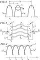
- FIG. 1 illustrates an example of a conventional optical frequency routing device.
- FIG. 2 is a graph showing the transmission coefficients T ik for the routing device of FIG. 1.
- FIG. 3 illustrates one embodiment of a routing arrangement constructed in accordance with the present invention.
- FIG. 4 is a graph showing the transmission coefficients for each of the distinct paths in the routing arrangement shown in FIG. 3.
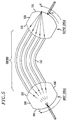
- FIG. 5 shows a conventional routing device such as shown in FIG. 1 illustrating the transmission of an image from an input port to an output port.
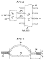
- FIG. 6 shows an alternative embodiment of the present invention in which the first frequency routing device is configured as a 1x2 routing device.
- FIG. 7 shows a Mach-Zehnder apparatus that may serve as the 1x2 routing device shown in FIG. 6.
- FIG. 8 shows an expanded view of a portion of the embodiment of the invention shown in FIG. 6 which incorporates the Mach-Zehnder apparatus shown in FIG. 7.
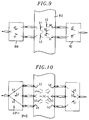
- FIG. 9 shows an alternative embodiment of the present invention which employs two Mach-Zehnder devices.
- FIG. 10 shows an embodiment of the present invention which is generalized from the embodiment shown in FIG. 9.
- FIG. 1 shows the pertinent details of a conventional frequency routing device.
- a plurality of output ports 30 extends from the output circle 97 of the free space region 98 and is connected to an optical grating 32.
- the optical grating 32 comprises a plurality of unequal length waveguides which provides a predetermined amount of path length difference to a corresponding plurality of input waveguides 34 connected to the input circle 33 of another free space region 46.
- the various input and output ports are formed from waveguides.
- These frequency routing devices operate as multiplexers and demultiplexers of optical frequencies. For example, if a signal of amplitude A is applied to input port 21 then signals of amplitudes AT11, AT12, ... AT 1N are produced at the output ports, where T ik is the value of the transmission coefficient for input port 2 i and output port 4 k . Additional details concerning these routing devices are found in the above-referenced patents.
- FIG. 2 The typical behavior of the routing device shown in FIG. 1 is illustrated in FIG. 2.
- This figure shows the set of transmission coefficients T 1k for the routing device for the particular input port 21 as a function of wavelength ⁇ .
- the channel spacing S indicated in FIG. 2 is defined as the wavelength separation between maximum peaks of adjacent transmission coefficients.
- the variation of each transmission coefficient as a function of wavelength is essentially periodic with a period X o , which is often referred to as the free spectral range of the device.
- the wavelengths ⁇ o , ⁇ 1 ..., ⁇ k of maximum transmission for each of the transmission coefficients are referred to as the center wavelengths.
- the transmission coefficients are substantially equal to unity at the center wavelengths if certain inherent losses are taken into account. In particular, the transmission coefficient will be equal to unity if wavelength independent losses are added thereto. These losses do not alter the principles upon which the present invention is based and hence they will be neglected in the discussion below.
- the channel spacing S is chosen to be large enough to ensure negligible crosstalk between different waveguides.
- a particular wavelength of maximum transmission such as ⁇ o in FIG. 2
- all other coefficients T ik are negligible.
- the various coefficients T ik are typically designed to be essentially non-overlapping, as in FIG. 2.
- the above-described conventional routing device has an undesirable feature, namely, that the passband is not very flat over its entire width W, as FIG. 2 indicates.
- FIG. 3 shows one embodiment of a routing arrangement constructed in accordance with the present invention.
- the routing arrangement is composed of two frequency routing devices 10 and 12 such as shown in FIG. 1.
- each routing device is configured as a 1xN routing device.
- the two routing devices may have differing numbers of input and output ports.
- P of the N output ports of the first routing device are optically coupled in series to P of the N input ports of the second routing device via a series of transmission waveguides 141, 142, ..., 14 p .
- the value of P may be equal to or less than the value of N.
- each of the individual routing devices 10 and 12 are configured to transit P distinct center wavelengths ⁇ 1, ⁇ 2, ..., ⁇ p , which are typically, but not necessarily, equally spaced apart from one another. Moreover, the routing devices 10 and 12 are configured so that adjacent ones of each of the passbands overlap, such as indicated in FIG. 2. This overlap allows transmission to occur at all wavelengths between ⁇ i and ⁇ i+1 .
- the first routing device 10 demultiplexes a signal directed to its input port 2 in the manner described above. If a multiplexed signal composed of wavelengths ⁇ 1, ⁇ 2, ..., ⁇ p is directed to input port 2 of the first routing device 10, each wavelength will be directed to a respective one of the transmission lines 141, 142, ..., 14 p . The transmission lines then direct the wavelengths to the input ports of the second routing device 12, which multiplexes the wavelengths so that they appear on output port 4.
- the routing arrangement shown in FIG. 3 contains p distinct optical paths between the input port 2 of the first routing device 2 and the output port 4 of the second routing device 12.
- Each path corresponds to one of the p transmission lines and each path is characterized by a distinct transmission coefficient t.
- the transmission coefficients t1, t2, ..., t p each have an amplitude of approximately unity at the center wavelengths ⁇ 1, ⁇ 2, ..., ⁇ p .
- the total transmission coefficient T of the device is therefore equal to the sum of the individual coefficients:
- the total transmission coefficient T will exhibit p maxima, which each occur at one of the center wavelengths ⁇ 1, ⁇ 2, ..., ⁇ p .
- FIG. 4 shows the transmission coefficients t1, t2, ..., t p as a function of wavelength. As FIG. 4 indicates, between each pair of adjacent maxima there is a wavelength for which the total transmission coefficient has a minimum amplitude. These minima are produced at approximately the intermediate wavelengths ⁇ i + ⁇ i +1 2
- the total transmission coefficient T should have an amplitude of approximately unity at the center wavelengths ⁇ 1, ⁇ 2, ..., ⁇ p as well as the intermediate wavelengths halfway between them.
- the transmission coefficients for each of the center wavelengths ⁇ i should fulfill the following condition:
- a flat passband (i.e.,
- the transmission coefficients for the transmission lines 141, 142, ..., 14 p will all be in phase if they are all provided with the same group delay.
- the transmission lines 141, 142, ..., 14 p will all have transmission coefficients with the same group delay if their lengths are properly chosen so that an optical pulse directed from the input circle of the first routing device 10 to the output circle of the second routing device will require the same transit time for each of the paths p.
- the optical grating 32 serves as an imaging apparatus. At any particular wavelength, the grating 32 transmits a filtered image of some initial optical distribution from the input port 2 i of the routing device to the output circle 35 of the output free space region 36.
- FIG. 5 shows a known routing device in which an input image emanates from point A on the input circle 595 of the input free space region 598 and is transmitted to point A' on the output circle 535 of the output free space region 536.
- Point B on the output circle 535 of the output free space region 536 denotes the location of the output port through which the image is to be transmitted.
- the optical grating 532 comprises a plurality of waveguides in which adjacent waveguides have a constant path length difference between them.
- the image location A' varies as a function of wavelength. It is this variation that is responsible for the relationship between the transmission coefficients and wavelength shown in FIG. 2.
- a transmission coefficient of nearly unity will only result if A' substantially coincides with B.
- the image location A' must remain coincident with B for all wavelengths in the passband interval approximately defined between ⁇ i ⁇ ⁇ ⁇ ⁇ i+1 .
- the location A from which the input image emanates should vary with wavelength to maintain point A' substantially coincident with B. The following discussion will demonstrate how this requirement can be more optimally and flexibly achieved by the routing arrangement of the present invention.
- FIG. 6 shows one embodiment of the present invention in which a 1x2 frequency routing device 610 is coupled to a NxN routing device 612, where N > 2.
- a 1x2 frequency routing device is essentially equivalent to a Mach-Zehnder apparatus such as shown in FIG. 7.
- the Mach-Zehnder apparatus is composed of a Y-branch coupler 702 that is optically coupled to two waveguides 704 and 706 of unequal length.
- the waveguides 704 and 706 terminate in an output section 708 in which the waveguides 704 and 706 have a predetermined length and a predetermined spacing between them.
- the Y-branch coupler 702 serves as the input port of the input frequency routing device 610 and the ends of the waveguides 704 and 706 in the output section 708 serve as the two output ports of the input frequency routing device 610 that are respectively coupled to the transmission lines 6141 and 6142.
- the Y-branch coupler 702 transfers half of the power of the input signal to each of the waveguides 704 and 706. Because the waveguides 704 and 706 have different path lengths, they produce in the output section 708 a wavelength-dependent phase difference between the two halves of the signal propagating in each waveguide.
- the spacing between the waveguides 704 and 706 in the output section 708 and the lengths thereof are chosen so that the two waveguides 704 and 706 are strongly coupled.
- the length of the waveguides 704 and 706 in the output section 708 is chosen so that half of the power propagating in each of the waveguides 704 and 706 prior to reaching the output section 708 is subsequently transferred to the other waveguide.
- the output signal at the end of the output section 708 will be centered at the midpoint A o between the axial points A1 and A2 of the waveguides 704 and 706 since half the power is propagating in each arm. If the wavelength of the input signal is increased to ⁇ 2 so that the phase difference is decreased by ⁇ /2, the output signal is centered along axis A2.
- the output signal will be located along axis A1.
- the location about which the output signal is centered along a line perpendicular to the axes of the waveguides 704 and 706 continuously varies from A1 to A o to A2, respectively.
- FIG. 8 shows an expanded view of a portion of the embodiment of the invention shown in FIG. 6 in which the waveguides 704 and 706 of the Mach-Zehnder apparatus form the input ports of the second frequency routing device 612.
- the points A o , A1 and A2 discussed in connection with FIG. 7 are now located on the input circle 833 of the free space region 897 of the second frequency routing device 612.
- an input signal directed through the Mach-Zehnder apparatus provides an image on the input circle 833 of the second frequency routing device 612 at a location between A1 and A2 that is a periodic function of wavelength.
- the criterion for providing a flat passband with nearly unity transmission is that an input signal having a wavelength in the passband interval between ⁇ 1 and ⁇ 2 should be directed to point B on the output circle 835 of the output free space region 836 of the second frequency routing device 612, where point B denotes the location of the output port of interest.
- This criterion is simply the general criterion discussed above particularized to the situation shown in FIG. 8.
- the Mach-Zehnder apparatus should be arranged so that an input signal of wavelength ⁇ 1 is directed with nearly unity transmission from point A1 to point B and an input signal of wavelength ⁇ 2 is directed with nearly unity transmission from point A2 to point B.
- the difference can be eliminated by slightly increasing the width of the output port, for example, so that the transmission coefficient for ⁇ o is increased while the transmission coefficient for ⁇ 1 and ⁇ 2 is decreased. In this manner a passband that is as flat as is practically possible can be obtained.
- the routing arrangement shown in FIG. 8 may be configured to be tunable. If the two waveguides 704 and 706 of the Mach-Zehnder apparatus shown in FIG. 8 have substantially the same length, there will be no phase difference between the signals propagating therein. Since the phase difference between the signals is zero, the location of the signal on the input circle 833 of the free space region 897 of the second frequency routing device will remain stationary. If one of the waveguides 704 and 706 is provided with a phase shifter that can selectively shift the optical path length of the waveguide by a predetermined amount, a predetermined amount of relative phase shift can be imparted to the signals propagating therein.
- the location of the resulting signal on the input circle 833 of the second routing device 612 also can be predetermined. Moreover, by preselecting the location of the signal in this manner, the center wavelength of maximum transmission for any given transmission coefficient also can be preselected, thus providing tunability.
- the phase shifter provided in one of the arms of the Mach-Zehnder apparatus may be chosen from among a variety of different phase shifters.
- the phase shifter may be a heating element that changes the temperature of the waveguide which in turn causes a change in its optical path length.
- the polarization shift i.e., the splitting of each wavelength of maximum transmission into two distinct peaks corresponding to the two principal polarizations TE and TM
- strain birefringence can be reduced or even eliminated. This reduction is accomplished in a manner analogous to that employed in the tunable routing arrangement discussed above.
- a polarization shifter is incorporated into one of the waveguides of the Mach-Zehnder apparatus.
- the polarization shifter which may be of any type known to those of ordinary skill in the art, introduces a suitable birefringence into the waveguide.
- One technique for introducing such birefringence is disclosed, for example, in M. Kawachi, "Silica Waveguides on Silicon and their Application to Integrated-Optical Components," Optical and Quantum Electronics, 22 (1990) pp. 391-416.
- FIG. 9 shows another embodiment of the invention based on the embodiment shown in FIG. 6 in which a Mach-Zehnder apparatus is coupled to the inputs of an NxN routing device.
- the input ports of a second Mach-Zehnder apparatus 820 are coupled to two output ports of the frequency routing device 812.
- the first Mach-Zehnder apparatus 810 serves to provide an image on the input circle of the frequency routing device 812 at a location that is a periodic function of wavelength.
- the second Mach-Zehnder apparatus 820 receives the image from the output ports of the frequency routing device 812 in a manner completely analogous to the optical coupling between the first Mach-Zehnder apparatus 810 and the frequency routing device 812 discussed above in connection with FIG. 6. Accordingly, the location of the image on the input circle of the frequency routing device 812 and the location at which the second Mach-Zehnder apparatus 820 is capable of optimally receiving the image from the frequency routing device 812 are both predeterminable and controllable.
- the resulting arrangement shown in FIG. 9 provides a wide passband that includes three wavelengths of maximum transmission.
- the optical paths shown in FIG. 9 indicate how these maxima arise.
- the optical paths are labeled in accordance with the respective ones of the wavelengths ⁇ 1, ⁇ 2, ⁇ 3 traversed by that path.
- wavelength ⁇ 2 traverses two distinct paths in the frequency routing device 812 before being recombined in the second Mach-Zehnder apparatus 820.
- the embodiment of the invention shown in FIG. 9 may be generalized as shown in FIG. 10 by replacing the two Mach-Zehnder devices with frequency routing devices having more than two input and output ports.
- FIG. 10 shows that five wavelengths of maximum transmission arise when the three frequency routing devices have three ports that are coupled together. More generally, if the three routing devices such as shown in FIG. 10 have P ports coupled together, a total of 2P-1 wavelengths of maximum transmission can be provided within the passband.
Landscapes
- Physics & Mathematics (AREA)
- General Physics & Mathematics (AREA)
- Optics & Photonics (AREA)
- Engineering & Computer Science (AREA)
- Nonlinear Science (AREA)
- Computer Networks & Wireless Communication (AREA)
- Microelectronics & Electronic Packaging (AREA)
- Optical Communication System (AREA)
- Optical Integrated Circuits (AREA)
Applications Claiming Priority (2)
| Application Number | Priority Date | Filing Date | Title |
|---|---|---|---|
| US08/295,445 US5488680A (en) | 1994-08-24 | 1994-08-24 | Frequency routing device having a wide and substantially flat passband |
| US295445 | 1994-08-24 |
Publications (2)
| Publication Number | Publication Date |
|---|---|
| EP0702253A2 true EP0702253A2 (de) | 1996-03-20 |
| EP0702253A3 EP0702253A3 (de) | 1996-07-03 |
Family
ID=23137763
Family Applications (1)
| Application Number | Title | Priority Date | Filing Date |
|---|---|---|---|
| EP95305686A Ceased EP0702253A3 (de) | 1994-08-24 | 1995-08-15 | Frequenzablenkungsvorrichtung mit breitem und im wesentlichen flachen Durchlassband |
Country Status (7)
| Country | Link |
|---|---|
| US (1) | US5488680A (de) |
| EP (1) | EP0702253A3 (de) |
| JP (1) | JP3256418B2 (de) |
| KR (1) | KR960008352A (de) |
| AU (1) | AU3013995A (de) |
| CA (1) | CA2149559A1 (de) |
| MX (1) | MX9503581A (de) |
Cited By (14)
| Publication number | Priority date | Publication date | Assignee | Title |
|---|---|---|---|---|
| EP0911659A1 (de) * | 1997-10-27 | 1999-04-28 | Lucent Technologies Inc. | Optischer Einfüge/Abzweig-Multiplexer mit komplementären Stufen |
| EP0936483A3 (de) * | 1998-02-10 | 1999-09-22 | Lucent Technologies Inc. | Optischer Verzweiger mit koherenten Verbindungspfaden |
| EP0933664A3 (de) * | 1998-01-30 | 2000-03-29 | Lucent Technologies Inc. | Verbesserter abstimmbarer Sender mit Mach-Zehnder-Modulator |
| EP1089097A3 (de) * | 1999-09-30 | 2002-12-11 | Agere Systems Optoelectronics Guardian Corporation | Weichenanordnung aus Wellenleitergitter mit dupliziertem Tor und im wesentlichen flachen Durchlassband |
| WO2002088791A3 (en) * | 2001-04-25 | 2003-03-13 | Lightwave Microsystems Corp | Multimode interference coupler for wdm applications |
| EP0901025A3 (de) * | 1997-09-08 | 2003-10-15 | Lucent Technologies Inc. | Optisches Durchlassfilter |
| WO2002048761A3 (en) * | 2000-12-13 | 2003-10-16 | Alcatel Optronics Uk Ltd | Segmented waveguide flattening the passband of a phasar |
| WO2004001470A1 (en) * | 2002-06-19 | 2003-12-31 | Gemfire Europe Limited | Athermal arrayed waveguide grating |
| EP1091220A3 (de) * | 1999-09-02 | 2004-04-07 | International Business Machines Corporation | Verbreiterung der Brandbreite eines Wellenleitergitters |
| WO2004083112A1 (en) * | 2003-03-19 | 2004-09-30 | Phicon Investment Holdings (Pty) Ltd | Assembling system |
| EP1226461B1 (de) * | 1999-11-01 | 2006-01-11 | Gemfire Europe Limited | Phasar mit flacher durchlasskurve |
| WO2007041706A1 (en) * | 2005-10-06 | 2007-04-12 | Lucent Technologies Inc. | Method and apparatus for wavelength-selective switches and modulators |
| WO2007047739A1 (en) * | 2005-10-18 | 2007-04-26 | Lucent Technologies Inc. | Retangular-passband multiplexer |
| WO2008118270A1 (en) * | 2007-03-24 | 2008-10-02 | Lucent Technologies Inc. | Tunable optical dispersion compensating apparatus |
Families Citing this family (43)
| Publication number | Priority date | Publication date | Assignee | Title |
|---|---|---|---|---|
| EP0612164A1 (de) * | 1993-02-19 | 1994-08-24 | AT&T Corp. | Schnell abstimmbarer breitbandiger intergrierter optischer Filter |
| US5623571A (en) * | 1995-08-29 | 1997-04-22 | Lucent Technologies Inc. | Polarization compensated waveguide grating router |
| US6097517A (en) * | 1995-09-01 | 2000-08-01 | Oki Electric Industry Co., Ltd. | Wavelength router |
| US5680490A (en) * | 1995-09-08 | 1997-10-21 | Lucent Technologies Inc. | Comb splitting system and method for a multichannel optical fiber communication network |
| US5706377A (en) * | 1996-07-17 | 1998-01-06 | Lucent Technologies Inc. | Wavelength routing device having wide and flat passbands |
| US5742414A (en) * | 1996-09-24 | 1998-04-21 | At&T Corp. | Multiplicity of services via a wavelength division router |
| US5745616A (en) * | 1996-11-27 | 1998-04-28 | Lucent Technologies Inc. | Waveguide grating router and method of making same having relatively small dimensions |
| US5740289A (en) * | 1996-12-30 | 1998-04-14 | At&T Corp | Optical arrangement for amplifying WDM signals |
| US6049644A (en) * | 1997-05-13 | 2000-04-11 | Lucent Technologies Inc. | Optical routing device having a substantially flat passband |
| FI103619B1 (fi) * | 1997-05-26 | 1999-07-30 | Nokia Telecommunications Oy | Optinen multipleksointi ja demultipleksointi |
| US5889906A (en) * | 1997-05-28 | 1999-03-30 | Lucent Technologies Inc. | Signal router with coupling of multiple waveguide modes for provicing a shaped multi-channel radiation pattern |
| US5870512A (en) | 1997-05-30 | 1999-02-09 | Sdl, Inc. | Optimized interferometrically modulated array source |
| JPH1130730A (ja) * | 1997-07-11 | 1999-02-02 | Oki Electric Ind Co Ltd | 光合分波素子 |
| US6137939A (en) * | 1997-10-01 | 2000-10-24 | Lucent Technologies Inc. | Method and apparatus for reducing temperature-related spectrum shifts in optical devices |
| JP3309369B2 (ja) | 1998-02-05 | 2002-07-29 | 日本電信電話株式会社 | 光波長合分波器 |
| GB2334343A (en) * | 1998-02-13 | 1999-08-18 | Northern Telecom Ltd | Optical waveguide multiplexer/demultiplexer with diffraction gratings embracing one another |
| US6351581B1 (en) | 1998-03-17 | 2002-02-26 | Agere Systems Optoelectronics Guardian Corp. | Optical add-drop multiplexer having an interferometer structure |
| US5937113A (en) * | 1998-04-17 | 1999-08-10 | National Research Council Of Canada | Optical grating-based device having a slab waveguide polarization compensating region |
| US6341186B1 (en) * | 1999-04-13 | 2002-01-22 | Qtera Corporation | Method and apparatus for the passband flattening of dense wavelength division optical filters |
| US6587615B1 (en) | 1999-05-11 | 2003-07-01 | Jds Fitel Inc. | Wavelength multiplexer-demultiplexer having a wide flat response within the spectral passband |
| US6421478B1 (en) | 1999-05-11 | 2002-07-16 | Jds Fitel Inc. | Tapered MMI coupler |
| US6351583B1 (en) * | 2000-01-28 | 2002-02-26 | Agere Systems Guardian Corp. | Multiple laser wavelength stabilization |
| US6421481B1 (en) | 2000-02-04 | 2002-07-16 | Zolo Technologies, Inc. | Apparatus and method for producing a flat-topped filter response for diffraction grating (De) multiplexer |
| US7509048B2 (en) * | 2001-07-20 | 2009-03-24 | Essex Corporation | Method and apparatus for optical signal processing using an optical tapped delay line |
| US6728446B2 (en) * | 2001-07-26 | 2004-04-27 | Lucent Technologies Inc. | Compact wavelength routing device having substantially flat passband |
| JP2003172830A (ja) * | 2001-12-04 | 2003-06-20 | Fujitsu Ltd | 光合分波器 |
| US7085438B2 (en) * | 2002-12-06 | 2006-08-01 | Nippon Telegraph And Telephone Corporation | Optical multi/demultiplexing circuit equipped with phase generating device |
| US7283700B2 (en) | 2005-11-02 | 2007-10-16 | Corrado Pietro Dragone | Optical router using stationary imaging |
| DK1857846T3 (da) * | 2006-05-19 | 2017-05-22 | Lumentum Operations Llc | Asymmetric Mach-Zehnder Interferometer Having a Reduced Drive Voltage Coupled to a Compact Low-Loss Arrayed Waveguide Grating |
| US7373039B1 (en) * | 2006-12-28 | 2008-05-13 | Lucent Technologies Inc. | Low-ripple optical device |
| US8236751B2 (en) * | 2007-03-07 | 2012-08-07 | The Johns Hopkins University | Methods of increasing muscle mass using follistatin-like related gene (FLRG) |
| JP5040642B2 (ja) * | 2007-12-27 | 2012-10-03 | 凸版印刷株式会社 | 回折構造形成体の製造方法 |
| JP5457661B2 (ja) | 2008-07-14 | 2014-04-02 | 日本電信電話株式会社 | 光波長合分波回路 |
| US7724991B1 (en) * | 2009-01-31 | 2010-05-25 | Alcatel-Lucent Usa Inc. | Compact optical receiver |
| EP2479593B1 (de) | 2009-09-18 | 2015-07-29 | Nippon Telegraph And Telephone Corporation | Optische multiplexer/demultiplexer-schaltung |
| US8204346B2 (en) * | 2009-11-21 | 2012-06-19 | Corrado Pietro Dragone | Optical router with nearly ideal performance |
| JP5244085B2 (ja) * | 2009-12-22 | 2013-07-24 | Nttエレクトロニクス株式会社 | 平面光波回路及び平面光波回路の製造方法 |
| US8594473B2 (en) * | 2010-02-20 | 2013-11-26 | Corrado Pietro Dragone | Optical router with stationary response and increased number of channels |
| US8326101B2 (en) | 2010-07-13 | 2012-12-04 | Corrado Pietro Dragone | Optical router with nearly ideal performance and increased number of channels |
| JP2015001626A (ja) * | 2013-06-14 | 2015-01-05 | Nttエレクトロニクス株式会社 | 光波長合分波回路 |
| JP6428146B2 (ja) | 2014-10-22 | 2018-11-28 | 日本電気株式会社 | 光導波路デバイス及びその製造方法 |
| JP2017142335A (ja) * | 2016-02-09 | 2017-08-17 | 沖電気工業株式会社 | 光合分波素子及びアレイ導波路回折格子型光波長フィルタ |
| JP7206528B2 (ja) | 2019-08-01 | 2023-01-18 | 日本電信電話株式会社 | 光波長合分波回路 |
Family Cites Families (8)
| Publication number | Priority date | Publication date | Assignee | Title |
|---|---|---|---|---|
| US5002350A (en) * | 1990-02-26 | 1991-03-26 | At&T Bell Laboratories | Optical multiplexer/demultiplexer |
| US5136671A (en) * | 1991-08-21 | 1992-08-04 | At&T Bell Laboratories | Optical switch, multiplexer, and demultiplexer |
| NL9101835A (nl) * | 1991-11-01 | 1993-06-01 | Nederland Ptt | Geintegreerde optische component. |
| JPH05346515A (ja) * | 1992-06-15 | 1993-12-27 | Nippon Telegr & Teleph Corp <Ntt> | 光遅延等化器 |
| US5339157A (en) * | 1993-02-19 | 1994-08-16 | At&T Bell Laboratories | Rapidly tunable integrated optical filter |
| US5373516A (en) * | 1993-02-19 | 1994-12-13 | At&T Corp. | Rapidly tunable wideband integrated laser |
| US5367586A (en) * | 1993-03-26 | 1994-11-22 | At&T Bell Laboratories | Optical delay line |
| US5412744A (en) * | 1994-05-02 | 1995-05-02 | At&T Corp. | Frequency routing device having a wide and substantially flat passband |
-
1994
- 1994-08-24 US US08/295,445 patent/US5488680A/en not_active Expired - Lifetime
-
1995
- 1995-05-17 CA CA002149559A patent/CA2149559A1/en not_active Abandoned
- 1995-08-15 EP EP95305686A patent/EP0702253A3/de not_active Ceased
- 1995-08-16 JP JP22960295A patent/JP3256418B2/ja not_active Expired - Fee Related
- 1995-08-21 MX MX9503581A patent/MX9503581A/es unknown
- 1995-08-21 AU AU30139/95A patent/AU3013995A/en not_active Abandoned
- 1995-08-23 KR KR1019950026074A patent/KR960008352A/ko not_active Withdrawn
Non-Patent Citations (1)
| Title |
|---|
| None |
Cited By (15)
| Publication number | Priority date | Publication date | Assignee | Title |
|---|---|---|---|---|
| EP0901025A3 (de) * | 1997-09-08 | 2003-10-15 | Lucent Technologies Inc. | Optisches Durchlassfilter |
| EP0911659A1 (de) * | 1997-10-27 | 1999-04-28 | Lucent Technologies Inc. | Optischer Einfüge/Abzweig-Multiplexer mit komplementären Stufen |
| EP0933664A3 (de) * | 1998-01-30 | 2000-03-29 | Lucent Technologies Inc. | Verbesserter abstimmbarer Sender mit Mach-Zehnder-Modulator |
| EP0936483A3 (de) * | 1998-02-10 | 1999-09-22 | Lucent Technologies Inc. | Optischer Verzweiger mit koherenten Verbindungspfaden |
| EP1091220A3 (de) * | 1999-09-02 | 2004-04-07 | International Business Machines Corporation | Verbreiterung der Brandbreite eines Wellenleitergitters |
| EP1089097A3 (de) * | 1999-09-30 | 2002-12-11 | Agere Systems Optoelectronics Guardian Corporation | Weichenanordnung aus Wellenleitergitter mit dupliziertem Tor und im wesentlichen flachen Durchlassband |
| EP1226461B1 (de) * | 1999-11-01 | 2006-01-11 | Gemfire Europe Limited | Phasar mit flacher durchlasskurve |
| WO2002048761A3 (en) * | 2000-12-13 | 2003-10-16 | Alcatel Optronics Uk Ltd | Segmented waveguide flattening the passband of a phasar |
| US6563988B2 (en) | 2001-04-25 | 2003-05-13 | Lightwave Microsystems Corporation | Optical apparatus and method having predetermined group velocity dispersion |
| WO2002088791A3 (en) * | 2001-04-25 | 2003-03-13 | Lightwave Microsystems Corp | Multimode interference coupler for wdm applications |
| WO2004001470A1 (en) * | 2002-06-19 | 2003-12-31 | Gemfire Europe Limited | Athermal arrayed waveguide grating |
| WO2004083112A1 (en) * | 2003-03-19 | 2004-09-30 | Phicon Investment Holdings (Pty) Ltd | Assembling system |
| WO2007041706A1 (en) * | 2005-10-06 | 2007-04-12 | Lucent Technologies Inc. | Method and apparatus for wavelength-selective switches and modulators |
| WO2007047739A1 (en) * | 2005-10-18 | 2007-04-26 | Lucent Technologies Inc. | Retangular-passband multiplexer |
| WO2008118270A1 (en) * | 2007-03-24 | 2008-10-02 | Lucent Technologies Inc. | Tunable optical dispersion compensating apparatus |
Also Published As
| Publication number | Publication date |
|---|---|
| EP0702253A3 (de) | 1996-07-03 |
| JP3256418B2 (ja) | 2002-02-12 |
| US5488680A (en) | 1996-01-30 |
| CA2149559A1 (en) | 1996-02-25 |
| MX9503581A (es) | 1997-05-31 |
| KR960008352A (ko) | 1996-03-22 |
| JPH0869021A (ja) | 1996-03-12 |
| AU3013995A (en) | 1996-03-07 |
Similar Documents
| Publication | Publication Date | Title |
|---|---|---|
| US5488680A (en) | Frequency routing device having a wide and substantially flat passband | |
| EP0681195B1 (de) | Frequenzweglenkungsvorrichtung mit breitbandigem und im wesentlichem flachen Durchlassband | |
| US5446809A (en) | All fiber wavelength selective optical switch | |
| US5953467A (en) | Switchable optical filter | |
| US6466341B1 (en) | Add/drop filter for a multi-wavelength lightwave system | |
| JP3537344B2 (ja) | 光アッド−ドロップ・マルチプレクサ | |
| EP0649040B1 (de) | Optischer Bandpass-Filter | |
| JP3448182B2 (ja) | 全光ファイバ製光ルータ | |
| EP0655874A2 (de) | Schnelles abstimmbares Kanalentnahmefilter | |
| JPH1062826A (ja) | 光学ルータ | |
| US5526153A (en) | Optical channel adding/dropping filter | |
| JPH10164021A (ja) | 波長多重通信用光回路及びこれを含む光伝送通信システム | |
| US20020150329A1 (en) | Multi-channel wavelength division multiplexer/demultiplexer | |
| CN114924357A (zh) | 一种基于级联马赫-曾德干涉仪结构的波分复用光延时线 | |
| US6597841B1 (en) | Multi-output arrayed waveguide grating demultiplexer | |
| EP1089479A2 (de) | Add/drop-Multiplexer für Wellenlängenmultiplexierung | |
| KR100442663B1 (ko) | 광 회선분배 시스템 | |
| KR20010085802A (ko) | 동조가능 애드/드롭 멀티플렉서 | |
| EP1089097A2 (de) | Weichenanordnung aus Wellenleitergitter mit dupliziertem Tor und im wesentlichen flachen Durchlassband | |
| JPH11271559A (ja) | 光学装置 | |
| US6546167B1 (en) | Tunable grating optical device | |
| JP3347382B2 (ja) | 光アド・ドロップ波長多重分離装置 | |
| KR100687043B1 (ko) | 재구성이 가능한 광 분기 및 결합장치 | |
| JPH0954346A (ja) | 光分波装置 | |
| JPH10148792A (ja) | 波長多重光源 |
Legal Events
| Date | Code | Title | Description |
|---|---|---|---|
| PUAI | Public reference made under article 153(3) epc to a published international application that has entered the european phase |
Free format text: ORIGINAL CODE: 0009012 |
|
| AK | Designated contracting states |
Kind code of ref document: A2 Designated state(s): DE FR GB IT NL SE |
|
| PUAL | Search report despatched |
Free format text: ORIGINAL CODE: 0009013 |
|
| AK | Designated contracting states |
Kind code of ref document: A3 Designated state(s): DE FR GB IT NL SE |
|
| 17P | Request for examination filed |
Effective date: 19961211 |
|
| 17Q | First examination report despatched |
Effective date: 20010724 |
|
| APBN | Date of receipt of notice of appeal recorded |
Free format text: ORIGINAL CODE: EPIDOSNNOA2E |
|
| APBR | Date of receipt of statement of grounds of appeal recorded |
Free format text: ORIGINAL CODE: EPIDOSNNOA3E |
|
| APAA | Appeal reference recorded |
Free format text: ORIGINAL CODE: EPIDOS REFN |
|
| APAF | Appeal reference modified |
Free format text: ORIGINAL CODE: EPIDOSCREFNE |
|
| APBT | Appeal procedure closed |
Free format text: ORIGINAL CODE: EPIDOSNNOA9E |
|
| STAA | Information on the status of an ep patent application or granted ep patent |
Free format text: STATUS: THE APPLICATION HAS BEEN REFUSED |
|
| 18R | Application refused |
Effective date: 20051209 |