EP0702389A2 - Système de réduction de l'émission de champs électrique - Google Patents
Système de réduction de l'émission de champs électrique Download PDFInfo
- Publication number
- EP0702389A2 EP0702389A2 EP95306251A EP95306251A EP0702389A2 EP 0702389 A2 EP0702389 A2 EP 0702389A2 EP 95306251 A EP95306251 A EP 95306251A EP 95306251 A EP95306251 A EP 95306251A EP 0702389 A2 EP0702389 A2 EP 0702389A2
- Authority
- EP
- European Patent Office
- Prior art keywords
- field
- unwanted
- cancellation
- amplifier
- electric field
- Prior art date
- Legal status (The legal status is an assumption and is not a legal conclusion. Google has not performed a legal analysis and makes no representation as to the accuracy of the status listed.)
- Granted
Links
- 230000005684 electric field Effects 0.000 title claims abstract description 44
- 230000009467 reduction Effects 0.000 title description 5
- 230000004044 response Effects 0.000 claims abstract description 15
- 239000011248 coating agent Substances 0.000 claims description 7
- 238000000576 coating method Methods 0.000 claims description 7
- 230000008878 coupling Effects 0.000 claims description 7
- 238000010168 coupling process Methods 0.000 claims description 7
- 238000005859 coupling reaction Methods 0.000 claims description 7
- 238000000034 method Methods 0.000 claims description 7
- 238000001514 detection method Methods 0.000 claims description 6
- 239000012799 electrically-conductive coating Substances 0.000 claims description 2
- 238000010586 diagram Methods 0.000 description 9
- 238000010894 electron beam technology Methods 0.000 description 7
- 230000001360 synchronised effect Effects 0.000 description 7
- 230000004048 modification Effects 0.000 description 5
- 238000012986 modification Methods 0.000 description 5
- OKTJSMMVPCPJKN-UHFFFAOYSA-N Carbon Chemical compound [C] OKTJSMMVPCPJKN-UHFFFAOYSA-N 0.000 description 4
- 230000003750 conditioning effect Effects 0.000 description 3
- 238000004519 manufacturing process Methods 0.000 description 3
- 238000012546 transfer Methods 0.000 description 3
- 238000005516 engineering process Methods 0.000 description 2
- 230000009471 action Effects 0.000 description 1
- 230000032683 aging Effects 0.000 description 1
- 230000015556 catabolic process Effects 0.000 description 1
- 239000004020 conductor Substances 0.000 description 1
- 230000003247 decreasing effect Effects 0.000 description 1
- 238000006731 degradation reaction Methods 0.000 description 1
- 238000013461 design Methods 0.000 description 1
- 230000000694 effects Effects 0.000 description 1
- 239000000383 hazardous chemical Substances 0.000 description 1
- 231100000206 health hazard Toxicity 0.000 description 1
- 239000002184 metal Substances 0.000 description 1
- 230000003287 optical effect Effects 0.000 description 1
- 238000002360 preparation method Methods 0.000 description 1
- 230000005855 radiation Effects 0.000 description 1
- 238000011160 research Methods 0.000 description 1
- 238000012216 screening Methods 0.000 description 1
- 230000002459 sustained effect Effects 0.000 description 1
- 230000000007 visual effect Effects 0.000 description 1
- 238000004804 winding Methods 0.000 description 1
Images


Classifications
-
- H—ELECTRICITY
- H01—ELECTRIC ELEMENTS
- H01J—ELECTRIC DISCHARGE TUBES OR DISCHARGE LAMPS
- H01J29/00—Details of cathode-ray tubes or of electron-beam tubes of the types covered by group H01J31/00
- H01J29/003—Arrangements for eliminating unwanted electromagnetic effects, e.g. demagnetisation arrangements, shielding coils
-
- H—ELECTRICITY
- H01—ELECTRIC ELEMENTS
- H01J—ELECTRIC DISCHARGE TUBES OR DISCHARGE LAMPS
- H01J2229/00—Details of cathode ray tubes or electron beam tubes
- H01J2229/0007—Elimination of unwanted or stray electromagnetic effects
- H01J2229/0015—Preventing or cancelling fields leaving the enclosure
Definitions
- the present invention relates to a system for reducing electric field emissions by the application of cancellation fields.
- a conventional raster scanned cathode ray tube (CRT) display such as a television receiver or a computer visual display unit comprises circuitry that can generate electric fields of sufficient strength to radiate beyond the display.
- CTR raster scanned cathode ray tube
- Various studies have raised public concern about these electric fields and the possible health hazards associated with them.
- various standards have been introduced defining maximum emission levels which products claiming to meet these standards can emit.
- products can be tested to a standard developed and administered by TCO, the Swedish Confederation of Professional Employees.
- true RMS values of emissions in the frequency band from 2kHz to 400kHz are measured and must be less than 1 Volt/metre.
- a CRT display typically comprises horizontal and vertical electromagnetic deflection coils arranged on a yoke mounted around the neck of the CRT.
- currents having a sawtooth waveform flow through the coils to scan the electron beam or beams across the CRT screen in a raster pattern.
- the voltages across the deflection coils reach a peak during the retrace or flyback period of the sawtooth currents.
- the peak voltage signals have a large component of harmonics of the corresponding deflection frequencies.
- the electron beam or beams are accelerated from the neck of the CRT towards the screen by a "final anode” or Extra High Tension (EHT) voltage of typically 25kV for a colour display.
- the flow of electrons is referred to as "beam current".
- the EHT voltage is typically generated from a step up transformer synchronised to the line scan.
- the voltage pulse signal driving the primary of the transformer is derived from the peak voltage across the horizontal deflection coil.
- the voltage pulse signal is generated separately from the line scan signal, but may be synchronised to it, although not necessarily in phase.
- the output impedance of the EHT generator is sufficiently high that changes in beam current loading through screen content cause modulation of the EHT voltage. This is the primary source of radiated electric fields in front of the display. This modulation of the internal CRT final anode voltage is coupled through the CRT faceplate and transmitted through the intervening medium (air in this case) to the observation point.
- Electric field emissions from CRT displays can be reduced at the sides and back by enclosing the radiating conductors with grounded metal screens, and this is normal for multi-frequency displays.
- the screening necessary to reduce the emissions in front of the display is usually in the form of a conductive optical panel which is transparent to the light emitted by the CRT panel.
- the screen image is viewed through the panel which can diminish image quality.
- these panels are expensive to manufacture.
- US Patent 5,151,635 describes an apparatus and method of reducing these time varying electric fields by providing a cancellation field of equal magnitude but opposite polarity to those generated by the horizontal deflection circuit, degaussing circuit and other circuits are provided, along with radiating antennae for each of these cancellation fields.
- European Patent Application 0 523 741 describes a similar apparatus which senses the electric field associated with the deflection yoke and provides a signal to a radiating antennae.
- the electric field sensed from the deflection circuit is similar to the actual electric field emitted from the display and so some cancellation of the primary source of radiated electric fields in front of the display is achieved.
- such a system may not achieve cancellation of the field since although the two circuits are usually, but not always, synchronised, they may be distanced from each other in phase.
- Co-pending UK Patent Application No.9312297.6 describes an open loop active field cancellation system for a CRT display.
- the system comprises a detection antenna connected via a matching network to the input of an inverting amplifier.
- the output of the amplifier is connected via a tuning network to a radiating antenna.
- the detection antenna detects electric fields radiating from the CRT.
- the amplifier amplifies and inverts the signal from the detection antenna.
- the matching network conditions the output from the detection antenna to correct for the amplifier gain and phase characteristics in preparation for application of the inverted signal output from the amplifier to the radiating antenna.
- a problem with this system is that it requires difficult adjustment during manufacture. Furthermore, in the event of a display fitted with this system requiring a major field service, readjustment may be needed.
- the open loop topology of this system limits further reductions in electric field radiation. This is a particularly significant problem because the acceptable Electric field emission level may be reduced as research continues. Still furthermore, high precision components are needed to prevent performance degradation with ageing.
- an electric field cancellation system comprising a sensor for generating an input signal indicative of an unwanted electric field radiating from a source, a variable gain amplifier for amplifying the input signal to produce an output signal, a radiator for generating a cancellation electric field in anti-phase to the unwanted field in response to the output signal to at least partially cancel the unwanted field, feedback means for generating an error signal indicative of the difference between the cancellation field and the unwanted field, and control means for varying the gain of the amplifier to vary the output signal in response to the error signal.
- the system of the present invention provides negative feedback, closed loop cancellation.
- the cancelling field therefore tracks the unwanted field as the negative feedback loop tends to minimise the error signal.
- the variable gain control of the amplifier causes the amplifier to respond to unwanted electric field of very low magnitude. Therefore, difficult manual of the performance of the cancellation system during manufacture or field service is not required.
- control means comprises an antenna for generating the error signal on simultaneous detection of both the cancellation field and the unwanted field.
- control means comprises an RMS to DC convertor for converting the error signal into a DC control level for controlling the gain of the amplifier.
- the RMS to DC convertor advantageously generates a DC control level indicative of the total energy in any residual field remaining due to any difference between the cancellation field and the unwanted field.
- the sensor may conveniently comprise a sense coil for inductively coupling the input of the amplifier to the source.
- the senor may comprise a capacitive sense element for capacitively coupling the input of the amplifier to the source.
- the cancellation system of the present invention is especially useful for cancelling electric fields from a cathode ray display tube.
- the radiator may then conveniently comprise the electrically conductive "aquadag" coating on the exterior of the cathode ray tube.
- the radiator may comprise a conductive element at least partially surrounding the screen of the cathode ray tube.
- the radiator may conveniently comprise an at least partially electrically conductive coating on the screen of the cathode ray tube.
- a method for at least partially cancelling an unwanted electric field radiating from a source comprising: sensing the unwanted field; generating an input signal indicative of the unwanted field; amplifying, using a variable gain amplifier, the input signal to produce an output signal; generating a cancellation electric field in anti-phase to the unwanted field in response to the output signal to at least partially cancel the unwanted field; generating an error signal indicative of the difference between the cancellation field and the unwanted field; and, varying the gain of the amplifier to vary the output signal in response to the error signal.
- a typical CRT display comprises a CRT 3 supported by a bezel 105.
- Horizontal and vertical deflection coils are disposed around the neck of the CRT 3 in a yoke 110.
- the CRT is controlled by a drive circuit.
- the drive circuit comprises horizontal and vertical scan circuits 115 and 120 connected to the horizontal and vertical deflection coils respectively, a video amplifier 125 connected to the electron gun of the CRT 3, and a power supply 130 for supplying power from the mains at 135 to scan circuits 115 and 120 and video amplifier 125 via supply rails Vs and 0V.
- Horizontal deflection circuit 115 comprises an integral EHT generator connected to the final anode of CRT 3.
- the EHT generator may be separate from the horizontal deflection circuit, but synchronised to the horizontal scan signal.
- the EHT generator comprises a step up transformer, the output of which is then rectified by high voltage diodes to produce, in conjunction with the CRT capacitance a DC output.
- a high resistance path to discharge the CRT capacitance (a bleed assembly) is present across the CRT 3.
- a degauss coil for demagnetising the CRT shadow mask. This coil operates generally whenever power is applied to the display.
- Thermistors whose resistance depends on temperature are used to cause the resultant current through the degauss coil to decay rapidly from a peak to switch on to a lower value. This lower value should have no visible effect on the screen, but nevertheless there is a residual mains frequency field emitted.
- power supply 130 receives power from the mains at 135.
- Line and frame scan circuits 115 and 120 generate line and frame sawtooth currents in the horizontal and vertical deflection coils to scan the three electron beams across CRT 3 in a raster pattern.
- Video amplifier 125 modulates the electron beam intensities with picture information in response to externally supplied red, green, and blue video signals.
- the sawtooth scan currents are synchronised to the input picture information by externally supplied horizontal and vertical synchronisation signals.
- the EHT transformer and CRT capacitance nominally cooperate to provide a constant DC voltage within the CRT.
- energy is drawn from the capacitance, causing a modulation of the DC voltage.
- This modulation signal is coupled through the CRT faceplate and transmitted, in the form of an undesirable time-varying electric field emission, through the intervening medium (air in most cases) to the observation point.
- an electric field cancellation of the present invention comprises a sensor 30 for generating an input signal I indicative of an unwanted electric field radiating from an electric field source such as CRT 3.
- a variable gain amplifier 5 is connected to sensor 30 for amplifying input signal I from sensor 30 to produce an output signal O.
- a radiator 20 is connected to amplifier 5 for generating a cancellation electric field C in anti-phase to unwanted field E in response to output signal O from amplifier 5 to at least partially cancel unwanted field E.
- Feedback means 10 generates an error signal F indicative of the difference between cancellation field C and unwanted field E.
- Control means 40 is connected to feedback means 10 for varying the gain of amplifier 5 to vary output signal O in response to the error signal F.
- sensor 30 is in the form of a sense coil 2 around a coupling cable 11 connecting the secondary winding of the EHT transformer 1 to CRT 3.
- Coil 2 is connected to the input of variable gain inverting amplifier 4.
- Radiator 20 is in the form of an aquadag conductive coating 8 on the exterior of CRT 3.
- Control means 40 includes an RMS to DC convertor 5 and a signal conditioning circuit 6.
- Amplifier 4 has a variable gain input connected to the output of convertor 5.
- Feedback means 10 includes a high impedance antenna 7. The input to convertor 5 is connected, through signal conditioning circuit 6 to antenna 7.
- sensor 2 detects the modulation signal from the current flowing in coupling cable 11.
- a replica of the modulation signal is induced by transformer action at the input of amplifier 4 via sense coil 2.
- Amplifier 4 forms part of the forward path of the closed loop cancellation apparatus. In the forward path, amplifier 4 amplifies and inverts the sensed modulation signal to produce at its output a cancellation signal which is in anti-phase with the actual modulation signal.
- the cancellation signal is applied to aqua dag coating 8 via resistor 9.
- Coating 8 acts as a radiator, responding to application of the cancelation signal by radiating a correspondingly time-variant electric cancellation field. The cancelation field propagates through the display and destructively interferes with the unwanted field produced by the actual modulation signal.
- Antenna 7 detects both the phase and antiphase signals to generate a feedback voltage signal.
- the feedback signal is the vector sum of the phase and antiphase fields and is thus a measure of any residual field.
- Signal conditioning circuit 6 provides impedance matching of the input of convertor 5 to the output of antenna 7.
- convertor 5 In response to the feedback signal, convertor 5 generates at the variable gain input of amplifier 4 a DC control voltage level which is representative of the energy in the residual field. Changes in the control level produce corresponding changes in the gain of amplifier 4 thereby varying the cancellation field strength in sympathy with variations in the residual field. A negative feedback loop is thus provided, tending to minimise the residual field.
- a potentiometer is typically provided to permit manual optimisation of active electric field cancellation.
- no potentiometer adjustment required to optimise the performance of the closed loop system of the present invention because the feedback loop minimises unwanted field emission automatically.
- the closed loop system of the present invention may automatically reduce the residual field to significantly less than 1V/m.
- the negative feedback loop of the closed loop system of the present invention effectively provides fine gain control of amplifier 4, avoiding a requirement for time consuming and difficult manual adjustment.
- the feedback signal produced by antenna 7 is a function of the vector sum of the phase and antiphase electric fields.
- the feedback signal is converted to a DC control level by convertor 5.
- the DC control level tunes the gain of amplifier 4.
- the transfer function of amplifier 4 is such that a nominal gain of five is available when the DC control level, V rms , is zero.
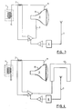
- FIG 8A illustrates typical waveforms of the phase E and antiphase C fields where the phase field strength E is greater than the antiphase field strength C.
- the corresponding control level, V rms is positive.
- the gain of amplifier 4 is thus increased, thereby increasing the antiphase field C, and leading to an overall reduction of the residual field.
- Figure 8B illustrates typical waveforms of the phase E and antiphase C fields where the phase field strength E is less than the antiphase field strength C.
- the corresponding control level, V rms is negative.
- the gain of amplifier 4 is thus reduced, thereby decreasing the antiphase field C, and leading to an overall reduction of the residual field.
- FIGs 8C and 8D illustrate the typical waveforms of the phase E and antiphase C fields where the phase field strength E equals the antiphase field strength C.
- the corresponding control level, V rms is zero.
- the gain of amplifier 4 is thus kept at the nominal level, maintaining the residual field at a constant minimum.
- the gradient of the curve indicative of the transfer function will determines the residual gain error of the feedback loop. Therefore, the curve is preferably very close to zero, lying at a slight angle relative to the X axis, so that minute residual fields detected by antenna 7 produce significant modification of the gain of amplifier 4.
- the time constant of the feedback loop is set to several frame periods of the display to give stability. It will be appreciated that the closed loop cancellation system of the present invention may be used to enhance a conventional open loop cancellation system by overcoming the aforementioned problem of manual tuning of the open loop performance and to allow only very low residual fields, if any, to radiate from the display.
- radiator 20 is in the form of an electrically conductive element 12 instead of the aquadag coating 8 of CRT 3.
- radiator 20 is provided by a high resistance "ESF" coating 13 on CRT 3.
- sensor 30 is in the form of an electrically conductive sensing element 14 attached to a non-shielded portion of CRT 3.
- the modulation signal is induced in the sense element by capacitive coupling.
- the circuit topology is effectively a first order servo system. This is unconditionally stable. Thus, it is not necessary to have a highly accurate RMS to DC convertor with good linearity. A simple, cost effective circuit will suffice.
Landscapes
- Physics & Mathematics (AREA)
- Electromagnetism (AREA)
- Details Of Television Scanning (AREA)
- Video Image Reproduction Devices For Color Tv Systems (AREA)
- Details Of Measuring And Other Instruments (AREA)
- Vessels, Lead-In Wires, Accessory Apparatuses For Cathode-Ray Tubes (AREA)
- Controls And Circuits For Display Device (AREA)
Applications Claiming Priority (2)
| Application Number | Priority Date | Filing Date | Title |
|---|---|---|---|
| GB9418570 | 1994-09-15 | ||
| GB9418570A GB2293299A (en) | 1994-09-15 | 1994-09-15 | Electric field emission reduction system |
Publications (3)
| Publication Number | Publication Date |
|---|---|
| EP0702389A2 true EP0702389A2 (fr) | 1996-03-20 |
| EP0702389A3 EP0702389A3 (fr) | 1996-11-27 |
| EP0702389B1 EP0702389B1 (fr) | 1999-03-03 |
Family
ID=10761353
Family Applications (1)
| Application Number | Title | Priority Date | Filing Date |
|---|---|---|---|
| EP95306251A Expired - Lifetime EP0702389B1 (fr) | 1994-09-15 | 1995-09-07 | Système de réduction de l'émission de champs électrique pour dispositif d'affichage à tube cathodique. |
Country Status (5)
| Country | Link |
|---|---|
| US (1) | US5534756A (fr) |
| EP (1) | EP0702389B1 (fr) |
| JP (1) | JP3251821B2 (fr) |
| DE (1) | DE69508017T2 (fr) |
| GB (1) | GB2293299A (fr) |
Cited By (1)
| Publication number | Priority date | Publication date | Assignee | Title |
|---|---|---|---|---|
| GB2309366A (en) * | 1996-01-16 | 1997-07-23 | Samsung Electronics Co Ltd | Device for cancelling stray electric fields of CRT displays |
Families Citing this family (12)
| Publication number | Priority date | Publication date | Assignee | Title |
|---|---|---|---|---|
| JPH08227666A (ja) * | 1995-02-20 | 1996-09-03 | Matsushita Electric Ind Co Ltd | Crtディスプレイの漏洩電界低減装置 |
| KR100190160B1 (ko) * | 1995-10-27 | 1999-06-01 | 윤종용 | 디스플레이 기기의 전계 차폐 회로 |
| US5814941A (en) * | 1997-02-19 | 1998-09-29 | Mag Technology Co., Ltd. | Device for eliminating low frequency radiation of monitor |
| KR19990052752A (ko) * | 1997-12-23 | 1999-07-15 | 전주범 | 모니터의 전자파 차단장치 |
| US7387772B1 (en) * | 1999-06-22 | 2008-06-17 | Immunimedics, Inc. | Chimeric, human and humanized anti-CSAP monoclonal antibodies |
| US7138103B2 (en) * | 1998-06-22 | 2006-11-21 | Immunomedics, Inc. | Use of bi-specific antibodies for pre-targeting diagnosis and therapy |
| US7405320B2 (en) | 1998-06-22 | 2008-07-29 | Immunomedics, Inc. | Therapeutic and diagnostic conjugates for use with multispecific antibodies |
| US7833528B2 (en) * | 1998-06-22 | 2010-11-16 | Immunomedics, Inc. | Use of multispecific, non-covalent complexes for targeted delivery of therapeutics |
| US6962702B2 (en) | 1998-06-22 | 2005-11-08 | Immunomedics Inc. | Production and use of novel peptide-based agents for use with bi-specific antibodies |
| SE515103C2 (sv) * | 1999-05-25 | 2001-06-11 | Enviromentor Ab | Aktivt sugtransformatorsystem samt användning av ett sådant |
| KR100524074B1 (ko) * | 2003-10-01 | 2005-10-26 | 삼성전자주식회사 | 베젤 구조를 가지는 전자기기 |
| US9819228B2 (en) * | 2013-03-01 | 2017-11-14 | Qualcomm Incorporated | Active and adaptive field cancellation for wireless power systems |
Citations (2)
| Publication number | Priority date | Publication date | Assignee | Title |
|---|---|---|---|---|
| US5151635A (en) | 1991-06-20 | 1992-09-29 | Apple Computer, Inc. | Apparatus and method for reducing the magnitude of time varying electric fields in CRT displays |
| EP0523741A1 (fr) | 1991-07-18 | 1993-01-20 | Kabushiki Kaisha Toshiba | Dispositif de tube à rayons cathodique |
Family Cites Families (8)
| Publication number | Priority date | Publication date | Assignee | Title |
|---|---|---|---|---|
| DK29385A (da) * | 1984-10-09 | 1986-04-10 | Viggo Berthelsen | Fremgangsmaade og indretning til eliminering af paavirkningen fra et magnetfelt og til beskyttelse mod samme |
| EP0348571A1 (fr) * | 1988-06-30 | 1990-01-03 | International Business Machines Corporation | Moniteur d'affichage à tube cathodique avec compensation des fuites du champ magnétique |
| US4996461A (en) * | 1989-09-07 | 1991-02-26 | Hughes Aircraft Company | Closed loop bucking field system |
| DE4123565C1 (fr) * | 1991-07-16 | 1992-09-17 | Tandberg Data A/S, Oslo, No | |
| SE469456B (sv) * | 1991-11-22 | 1993-07-05 | Nokia Data Ab | Foerfarande och anordning i en bildskaermsenhet foer att reducera elektriska vaexelfaelt i enhetens omgivning |
| GB2273230A (en) * | 1992-12-02 | 1994-06-08 | Ibm | Cancelling radiated electric fields in crt displays |
| US5396151A (en) * | 1993-06-28 | 1995-03-07 | Apple Computer, Inc. | Circuit for reducing ELF electric fields radiated from CRT devices |
| GB2283646A (en) * | 1993-10-30 | 1995-05-10 | Ibm | Reducing electric field emission from a CRT display |
-
1994
- 1994-09-15 GB GB9418570A patent/GB2293299A/en not_active Withdrawn
-
1995
- 1995-03-22 US US08/408,511 patent/US5534756A/en not_active Expired - Fee Related
- 1995-09-01 JP JP22487395A patent/JP3251821B2/ja not_active Expired - Fee Related
- 1995-09-07 EP EP95306251A patent/EP0702389B1/fr not_active Expired - Lifetime
- 1995-09-07 DE DE69508017T patent/DE69508017T2/de not_active Expired - Fee Related
Patent Citations (2)
| Publication number | Priority date | Publication date | Assignee | Title |
|---|---|---|---|---|
| US5151635A (en) | 1991-06-20 | 1992-09-29 | Apple Computer, Inc. | Apparatus and method for reducing the magnitude of time varying electric fields in CRT displays |
| EP0523741A1 (fr) | 1991-07-18 | 1993-01-20 | Kabushiki Kaisha Toshiba | Dispositif de tube à rayons cathodique |
Cited By (2)
| Publication number | Priority date | Publication date | Assignee | Title |
|---|---|---|---|---|
| GB2309366A (en) * | 1996-01-16 | 1997-07-23 | Samsung Electronics Co Ltd | Device for cancelling stray electric fields of CRT displays |
| GB2309366B (en) * | 1996-01-16 | 1999-12-29 | Samsung Electronics Co Ltd | Device for cancelling electric field of display |
Also Published As
| Publication number | Publication date |
|---|---|
| JP3251821B2 (ja) | 2002-01-28 |
| JPH08106273A (ja) | 1996-04-23 |
| DE69508017D1 (de) | 1999-04-08 |
| EP0702389B1 (fr) | 1999-03-03 |
| GB2293299A (en) | 1996-03-20 |
| GB9418570D0 (en) | 1994-11-02 |
| DE69508017T2 (de) | 1999-10-07 |
| US5534756A (en) | 1996-07-09 |
| EP0702389A3 (fr) | 1996-11-27 |
Similar Documents
| Publication | Publication Date | Title |
|---|---|---|
| EP0702389B1 (fr) | Système de réduction de l'émission de champs électrique pour dispositif d'affichage à tube cathodique. | |
| US5151635A (en) | Apparatus and method for reducing the magnitude of time varying electric fields in CRT displays | |
| EP0630036B1 (fr) | Tube à rayons cathodiques avec élimination des émissions de champ électrique | |
| US5404084A (en) | Method of and apparatus for canceling electric field | |
| CA1259127A (fr) | Circuit de suppression pour bloc d'alimentation d'appareil video | |
| US5432411A (en) | Electric field emission reduction apparatus | |
| US5614789A (en) | Apparatus and method of reducing varying electrical fields in video display terminals | |
| GB2273230A (en) | Cancelling radiated electric fields in crt displays | |
| JP2000102028A (ja) | フォ―カス電圧トラッキング回路 | |
| GB2313279A (en) | Video display appliance including a device for limiting electric field emitted from a cathode ray tube | |
| MXPA97003499A (en) | Video presentation instrument that includes a device to eliminate electric field emitted from a catodi ray tube | |
| US6215259B1 (en) | Apparatus for compensating for corner focus and brightness in cathode ray tube | |
| US5815361A (en) | Magnetic field shielding device in display | |
| KR100549831B1 (ko) | 음극선관 디스플레이 장치 | |
| JPH04288777A (ja) | 陰極線管用の電源 | |
| US6144416A (en) | Apparatus of shielding VLF electric field emitted from front face of CRT in video appliance | |
| JP3146061B2 (ja) | 陰極線管および陰極線管画像表示装置 | |
| RU2160510C2 (ru) | Видеодисплей со схемой подавления нежелательного излучения электронно-лучевой трубки | |
| JPH06103934A (ja) | 表示装置 | |
| GB2322270A (en) | Circuit for eliminating radiated electric field noise in a video display | |
| JPH05207404A (ja) | 陰極線管装置および陰極線管画像表示装置 | |
| JPH09325726A (ja) | Crt表示装置における漏洩電界低減装置 | |
| KR20020020361A (ko) | 영상표시기기의 광대역 스위칭 드라이브 보상회로 | |
| Hrytskiv | A Generalised View of the Problem of EMC for Cathode Ray Tubes | |
| JPH1074462A (ja) | 受像管装置 |
Legal Events
| Date | Code | Title | Description |
|---|---|---|---|
| PUAI | Public reference made under article 153(3) epc to a published international application that has entered the european phase |
Free format text: ORIGINAL CODE: 0009012 |
|
| AK | Designated contracting states |
Kind code of ref document: A2 Designated state(s): DE FR GB DE FR GB |
|
| PUAL | Search report despatched |
Free format text: ORIGINAL CODE: 0009013 |
|
| 17P | Request for examination filed |
Effective date: 19960827 |
|
| AK | Designated contracting states |
Kind code of ref document: A3 Designated state(s): DE FR GB |
|
| 17Q | First examination report despatched |
Effective date: 19970131 |
|
| GRAG | Despatch of communication of intention to grant |
Free format text: ORIGINAL CODE: EPIDOS AGRA |
|
| GRAG | Despatch of communication of intention to grant |
Free format text: ORIGINAL CODE: EPIDOS AGRA |
|
| GRAH | Despatch of communication of intention to grant a patent |
Free format text: ORIGINAL CODE: EPIDOS IGRA |
|
| GRAH | Despatch of communication of intention to grant a patent |
Free format text: ORIGINAL CODE: EPIDOS IGRA |
|
| GRAA | (expected) grant |
Free format text: ORIGINAL CODE: 0009210 |
|
| AK | Designated contracting states |
Kind code of ref document: B1 Designated state(s): DE FR GB |
|
| REF | Corresponds to: |
Ref document number: 69508017 Country of ref document: DE Date of ref document: 19990408 |
|
| ET | Fr: translation filed | ||
| PGFP | Annual fee paid to national office [announced via postgrant information from national office to epo] |
Ref country code: FR Payment date: 19990917 Year of fee payment: 5 |
|
| PLBE | No opposition filed within time limit |
Free format text: ORIGINAL CODE: 0009261 |
|
| STAA | Information on the status of an ep patent application or granted ep patent |
Free format text: STATUS: NO OPPOSITION FILED WITHIN TIME LIMIT |
|
| 26N | No opposition filed | ||
| PG25 | Lapsed in a contracting state [announced via postgrant information from national office to epo] |
Ref country code: FR Free format text: LAPSE BECAUSE OF NON-PAYMENT OF DUE FEES Effective date: 20010531 |
|
| REG | Reference to a national code |
Ref country code: FR Ref legal event code: ST |
|
| REG | Reference to a national code |
Ref country code: GB Ref legal event code: IF02 |
|
| PGFP | Annual fee paid to national office [announced via postgrant information from national office to epo] |
Ref country code: DE Payment date: 20030911 Year of fee payment: 9 |
|
| PGFP | Annual fee paid to national office [announced via postgrant information from national office to epo] |
Ref country code: GB Payment date: 20040902 Year of fee payment: 10 |
|
| PG25 | Lapsed in a contracting state [announced via postgrant information from national office to epo] |
Ref country code: DE Free format text: LAPSE BECAUSE OF NON-PAYMENT OF DUE FEES Effective date: 20050401 |
|
| PG25 | Lapsed in a contracting state [announced via postgrant information from national office to epo] |
Ref country code: GB Free format text: LAPSE BECAUSE OF NON-PAYMENT OF DUE FEES Effective date: 20050907 |
|
| GBPC | Gb: european patent ceased through non-payment of renewal fee |
Effective date: 20050907 |