EP0703606A2 - Procédé pour éviter le re-dépÔt de produits de gravure sur la surface de substrats pendant la rétro-gravure de tungstène au cours de la fabrication de circuits à haute densité d'intégration - Google Patents
Procédé pour éviter le re-dépÔt de produits de gravure sur la surface de substrats pendant la rétro-gravure de tungstène au cours de la fabrication de circuits à haute densité d'intégration Download PDFInfo
- Publication number
- EP0703606A2 EP0703606A2 EP95114752A EP95114752A EP0703606A2 EP 0703606 A2 EP0703606 A2 EP 0703606A2 EP 95114752 A EP95114752 A EP 95114752A EP 95114752 A EP95114752 A EP 95114752A EP 0703606 A2 EP0703606 A2 EP 0703606A2
- Authority
- EP
- European Patent Office
- Prior art keywords
- substrate
- etching
- stops
- retaining ring
- tungsten
- Prior art date
- Legal status (The legal status is an assumption and is not a legal conclusion. Google has not performed a legal analysis and makes no representation as to the accuracy of the status listed.)
- Ceased
Links
Images

Classifications
-
- H—ELECTRICITY
- H10—SEMICONDUCTOR DEVICES; ELECTRIC SOLID-STATE DEVICES NOT OTHERWISE PROVIDED FOR
- H10P—GENERIC PROCESSES OR APPARATUS FOR THE MANUFACTURE OR TREATMENT OF DEVICES COVERED BY CLASS H10
- H10P72/00—Handling or holding of wafers, substrates or devices during manufacture or treatment thereof
- H10P72/70—Handling or holding of wafers, substrates or devices during manufacture or treatment thereof for supporting or gripping
- H10P72/76—Handling or holding of wafers, substrates or devices during manufacture or treatment thereof for supporting or gripping using mechanical means, e.g. clamps or pinches
- H10P72/7604—Handling or holding of wafers, substrates or devices during manufacture or treatment thereof for supporting or gripping using mechanical means, e.g. clamps or pinches the wafers being placed on a susceptor, stage or support
- H10P72/7606—Handling or holding of wafers, substrates or devices during manufacture or treatment thereof for supporting or gripping using mechanical means, e.g. clamps or pinches the wafers being placed on a susceptor, stage or support characterised by edge clamping, e.g. clamping ring
-
- H—ELECTRICITY
- H10—SEMICONDUCTOR DEVICES; ELECTRIC SOLID-STATE DEVICES NOT OTHERWISE PROVIDED FOR
- H10P—GENERIC PROCESSES OR APPARATUS FOR THE MANUFACTURE OR TREATMENT OF DEVICES COVERED BY CLASS H10
- H10P95/00—Generic processes or apparatus for manufacture or treatments not covered by the other groups of this subclass
-
- H—ELECTRICITY
- H01—ELECTRIC ELEMENTS
- H01J—ELECTRIC DISCHARGE TUBES OR DISCHARGE LAMPS
- H01J2237/00—Discharge tubes exposing object to beam, e.g. for analysis treatment, etching, imaging
- H01J2237/02—Details
- H01J2237/022—Avoiding or removing foreign or contaminating particles, debris or deposits on sample or tube
Definitions
- the invention relates to a method for etching back substrate surfaces coated with tungsten in the manufacture of highly integrated circuits, in which the substrate is pressed against a cooled sample holder during the etching back by means of a retaining ring arranged on the edge of the substrate.
- the various conductive layers for example doped silicon substrate, polysilicon or metal tracks, are separated from one another by insulators (for example SiO2).
- insulators for example SiO2.
- the individual conductive layers must be contacted with one another at suitable locations.
- holes so-called contact holes or vias, are etched into the insulators, into which conductive material is then also introduced.
- CVD-W chemically vapor-deposited tungsten
- a known procedure consists first of all in the deposition of a CVD-W layer of tungsten hexafluoride WF6 and H2 or SiH4.
- This layer is deposited on a TiN or TiW base (adhesive layer, barrier) and grows on the entire substrate surface as well as on the perforated bottom and side walls until, in the case of the latter, the layer grows together.
- the etching back the conductive layer previously deposited on the horizontal substrate surface is completely removed again, so that in the ideal case the layer with conductive material completely filled contact holes or vias.
- tungsten etching back it is necessary that the substrate is pressed against a cooled sample holder (pedestal) by means of a holding device, the holding or clamp ring. Machining tolerances and surface roughness results in a microscopic cavity or gap between pedestal and substrate, which is detrimental to good substrate cooling.
- the cavity between the substrate and the pedestal is therefore filled with helium, which is supplied through the pedestal. So that no helium gets on the front of the substrate and that the substrate is not pressed away from the pedestal by the helium that is fed in, the substrate is pressed against the sample holder with a retaining ring, this retaining ring so far being designed so that it completely surrounds the substrate.
- the etching back step is typically carried out in a plasma containing F and / or Cl, the most important influences of the process parameters on various target variables being known per se.
- the aim is not only to fill the contact holes or vias with conductive material, but also to have a substrate surface that is free of tungsten residues after the tungsten etching back.
- This requirement for the etch back process to completely remove the conductive material from the substrate surface is important in order to avoid short circuits between subsequently generated tracks.
- the etching back step is extended in time, ie it is overetched until the surface of the TiN or TiW base (adhesive layer, barrier) is free of tungsten residues.
- the adhesive layer is thinned and in some cases even completely removed locally, in particular in the edge region.
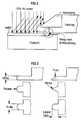
- the freed up Etched products are deposited on the edge of the substrate. As can be seen from FIG. 1, this precipitation is concentrated in a region of the substrate holding device which comes into direct contact with the substrate. If the substrate is now brought into the atmosphere after the etching-back process has ended, the precipitate mixes with the oxygen contained in the ambient air. This mixture is also no longer removed in subsequent work steps (for example water rinsing) which are contained in the further process flow.
- the present invention is therefore based on the object of providing a method of the type specified at the outset which helps to avoid problems with the undesired re-deposition described.
- the substrate edge is only held locally at stops distributed over the circumference by the retaining ring, and that these stops are designed to be free of backlash compared to the etching products released during the etching back, so that the etching products flow past the stops and specifically outside be deposited on the substrate surface.
- the invention is based on the knowledge that the harmful deposition behavior is solely attributable to the substrate holder and that the described effect of the deposition of etching products on the substrate surface in the immediate vicinity of a substrate holding ring can be avoided entirely by changing the substrate holding ring in such a way that the etching products are targeted outside be deposited on the substrate surface. This is achieved by working out the retaining ring so that the substrate is only local or is held selectively by the substrate holder. One could say that according to the invention the substrate is only held by individual “fingers”. The shape and dimensions of the fingers and the retaining ring are decisive for the targeted deposition of the undesired etching products outside the substrate.
- At least three of the stops extending finger-shaped to the edge of the substrate should be provided on the retaining ring.
- a comb-like variety of stops is also possible.
- the front end of the finger-shaped stop, which extends to the substrate edge is only indicated by an empty rectangle for better understanding; the past the stops-or etching gas / products flowing between them is deposited as shown outside of the substrate surface. This process is only to be emphasized by the circle marking in FIG. 2, which has no other meaning. A backflow of the etched products at the stops, which would lead to an undesirable deposit there, can be avoided by the formation of the stops shown in FIG.
- a width, height and length of at most a few millimeters should be selected for the finger-shaped stops, in particular the width and height should be in the range of approximately 2 mm. If the stops were too narrow, an excessive holding force would act locally on the wafer, so that there would be a risk of damage. If the length is too long, the gas would have to flow too far, on the other hand a minimum height is required so that the gas can flow through unhindered. To avoid backflow, it is advantageous to flatten the finger-shaped stops towards their ends on the substrate side.
- FIG. 2 also shows an additional cover ring resting on the retaining ring, which covers the substrate edge at a distance. This wearing part protects the retaining ring or pedestal from the influence of plasma.
- the substrate holding ring can be used, for example, in a CVD and etch-back system of the type AMT P5000 from Applied Materials.
Landscapes
- Drying Of Semiconductors (AREA)
- Container, Conveyance, Adherence, Positioning, Of Wafer (AREA)
- ing And Chemical Polishing (AREA)
Applications Claiming Priority (2)
| Application Number | Priority Date | Filing Date | Title |
|---|---|---|---|
| DE4433538 | 1994-09-20 | ||
| DE4433538A DE4433538A1 (de) | 1994-09-20 | 1994-09-20 | Verfahren zur Vermeidung der Re-Deposition von Ätzprodukten auf Substratoberflächen während des Wolfram-Rückätzprozesses bei der Herstellung hochintegrierter Schaltungen |
Publications (2)
| Publication Number | Publication Date |
|---|---|
| EP0703606A2 true EP0703606A2 (fr) | 1996-03-27 |
| EP0703606A3 EP0703606A3 (fr) | 1998-03-11 |
Family
ID=6528717
Family Applications (1)
| Application Number | Title | Priority Date | Filing Date |
|---|---|---|---|
| EP95114752A Ceased EP0703606A3 (fr) | 1994-09-20 | 1995-09-19 | Procédé pour éviter le re-dépÔt de produits de gravure sur la surface de substrats pendant la rétro-gravure de tungstène au cours de la fabrication de circuits à haute densité d'intégration |
Country Status (5)
| Country | Link |
|---|---|
| US (1) | US6380094B1 (fr) |
| EP (1) | EP0703606A3 (fr) |
| JP (1) | JPH08111406A (fr) |
| DE (1) | DE4433538A1 (fr) |
| TW (1) | TW317964U (fr) |
Cited By (1)
| Publication number | Priority date | Publication date | Assignee | Title |
|---|---|---|---|---|
| EP1117127A1 (fr) * | 2000-01-17 | 2001-07-18 | Infineon Technologies AG | Dispositif pour le support d'objets en forme de disque dans un sytème de traitement |
Families Citing this family (6)
| Publication number | Priority date | Publication date | Assignee | Title |
|---|---|---|---|---|
| US7074298B2 (en) * | 2002-05-17 | 2006-07-11 | Applied Materials | High density plasma CVD chamber |
| KR101141577B1 (ko) * | 2010-07-07 | 2012-06-08 | (주)세미머티리얼즈 | 태양전지의 플라즈마 텍스처링 장치 및 방법 |
| US9040432B2 (en) | 2013-02-22 | 2015-05-26 | International Business Machines Corporation | Method for facilitating crack initiation during controlled substrate spalling |
| CN104051293A (zh) * | 2013-03-13 | 2014-09-17 | 稳懋半导体股份有限公司 | 晶圆边缘保护装置 |
| US9502278B2 (en) | 2013-04-22 | 2016-11-22 | International Business Machines Corporation | Substrate holder assembly for controlled layer transfer |
| GB201419210D0 (en) * | 2014-10-29 | 2014-12-10 | Spts Technologies Ltd | Clamp assembly |
Family Cites Families (8)
| Publication number | Priority date | Publication date | Assignee | Title |
|---|---|---|---|---|
| US5024747A (en) * | 1979-12-21 | 1991-06-18 | Varian Associates, Inc. | Wafer coating system |
| US4306731A (en) * | 1979-12-21 | 1981-12-22 | Varian Associates, Inc. | Wafer support assembly |
| US5215619A (en) * | 1986-12-19 | 1993-06-01 | Applied Materials, Inc. | Magnetic field-enhanced plasma etch reactor |
| EP0312986A1 (fr) | 1987-10-22 | 1989-04-26 | Siemens Aktiengesellschaft | Procédé de décapage du tungstène avec une sous-couche de nitrure de titane dans des trous de contact de circuits intégrés |
| JPH0231420A (ja) | 1988-05-20 | 1990-02-01 | Tegal Corp | プラズマリアクタ用ウエハークランプ装置 |
| US4898639A (en) * | 1989-04-14 | 1990-02-06 | Bjorne Enterprises, Inc. | Wafer retention device |
| US5292399A (en) | 1990-04-19 | 1994-03-08 | Applied Materials, Inc. | Plasma etching apparatus with conductive means for inhibiting arcing |
| US5292558A (en) * | 1991-08-08 | 1994-03-08 | University Of Texas At Austin, Texas | Process for metal deposition for microelectronic interconnections |
-
1994
- 1994-09-20 DE DE4433538A patent/DE4433538A1/de not_active Withdrawn
-
1995
- 1995-08-12 TW TW085214353U patent/TW317964U/zh unknown
- 1995-09-18 US US08/529,322 patent/US6380094B1/en not_active Expired - Lifetime
- 1995-09-19 EP EP95114752A patent/EP0703606A3/fr not_active Ceased
- 1995-09-19 JP JP26474995A patent/JPH08111406A/ja active Pending
Non-Patent Citations (1)
| Title |
|---|
| None |
Cited By (2)
| Publication number | Priority date | Publication date | Assignee | Title |
|---|---|---|---|---|
| EP1117127A1 (fr) * | 2000-01-17 | 2001-07-18 | Infineon Technologies AG | Dispositif pour le support d'objets en forme de disque dans un sytème de traitement |
| WO2001054170A1 (fr) * | 2000-01-17 | 2001-07-26 | Infineon Technologies Ag | Mecanisme destine a supporter des objets en forme de disque dans un systeme de traitement |
Also Published As
| Publication number | Publication date |
|---|---|
| TW317964U (en) | 1997-10-11 |
| EP0703606A3 (fr) | 1998-03-11 |
| US6380094B1 (en) | 2002-04-30 |
| DE4433538A1 (de) | 1996-03-21 |
| JPH08111406A (ja) | 1996-04-30 |
Similar Documents
| Publication | Publication Date | Title |
|---|---|---|
| DE1621599C2 (de) | Einrichtung zum Abtragen von Verunrei nigungen einer auf einem Halbleiterkörper aufgebrachten metallischen Schicht im Be reich von kleinen Offnungen einer Isolier schicht durch Kathodenzerstäubung | |
| DE69825630T2 (de) | Fokusringe | |
| DE69513758T2 (de) | Ätzverfahren und Plasmareaktor zur Durchführung desselben | |
| DE69625974T2 (de) | Verfahren und Struktur zur Verbesserung der Flüssigkeitsströmung für Wärmetransport in elektrostatische Halter | |
| DE69301942T2 (de) | Verfahren und Gerät zur Beseitigung von Oberflächenbeschädigungen in Halbleiter-Materialien mittels Plasma-Ätzen | |
| DE69401549T2 (de) | Plasma-Behandlungsgerät | |
| DE69403816T2 (de) | Gerät und Verfahren zu erhöhter induktiver Ankopplung an Plasmen mit reduzierter Zerstäubungskontamination | |
| DE69124411T2 (de) | Vorrichtung zur Kontrolle der Kontaminierung in einen mit einer Spannung betriebenen Elektroden versehenen Gerät | |
| DE69409459T2 (de) | Verfahren und Gerät zur Plasmabearbeitung von Werkstücken | |
| DE60316717T2 (de) | Verfahren zum herstellen einer halbleiter anordnung durch ein plasmaätzverfahren | |
| DE3609681A1 (de) | Vorrichtung und verfahren zur duennfilmerzeugung | |
| DE3140890C2 (de) | Photolithographisches Verfahren zum Herstellen einer integrierten Schaltungsvorrichtung | |
| DE4219016A1 (de) | Verfahren, durch das eine vertiefung im wesentlichen gefuellt wird | |
| DE69211175T2 (de) | Sputterverfahren zum Bilden einer Aluminiumschicht auf einem gestuften Wafer | |
| DE4105103C2 (fr) | ||
| DE69733962T2 (de) | Plasma-ätzmethode | |
| DE4130391A1 (de) | Verfahren zum plasmaaetzen | |
| DE602004008429T2 (de) | Magnettunnelübergang-stapelablagerung in zwei schritten | |
| DE4039853A1 (de) | Vorrichtung und verfahren zur oberflaechenreinigung | |
| DE10340848A1 (de) | Herstellungsverfahren für eine Halbleitereinrichtung | |
| EP0703606A2 (fr) | Procédé pour éviter le re-dépÔt de produits de gravure sur la surface de substrats pendant la rétro-gravure de tungstène au cours de la fabrication de circuits à haute densité d'intégration | |
| DE2432719A1 (de) | Verfahren zum erzeugen von feinen strukturen aus aufdampfbaren materialien auf einer unterlage | |
| DE102013111860A1 (de) | Prozesswerkzeuge und Verfahren zur Bildung von Vorrichtungen unter Verwendung von Prozesswerkzeugen | |
| US5391513A (en) | Wet/dry anti-fuse via etch | |
| DE10226603A1 (de) | Verfahren zum Strukturieren einer Siliziumschicht sowie dessen Verwendung zur Herstellung einer integrierten Halbleiterschaltung |
Legal Events
| Date | Code | Title | Description |
|---|---|---|---|
| PUAI | Public reference made under article 153(3) epc to a published international application that has entered the european phase |
Free format text: ORIGINAL CODE: 0009012 |
|
| AK | Designated contracting states |
Kind code of ref document: A2 Designated state(s): DE FR GB IE IT |
|
| PUAL | Search report despatched |
Free format text: ORIGINAL CODE: 0009013 |
|
| AK | Designated contracting states |
Kind code of ref document: A3 Designated state(s): DE FR GB IE IT |
|
| 17P | Request for examination filed |
Effective date: 19980406 |
|
| RAP1 | Party data changed (applicant data changed or rights of an application transferred) |
Owner name: INFINEON TECHNOLOGIES AG |
|
| 17Q | First examination report despatched |
Effective date: 20020121 |
|
| STAA | Information on the status of an ep patent application or granted ep patent |
Free format text: STATUS: THE APPLICATION HAS BEEN REFUSED |
|
| 18R | Application refused |
Effective date: 20020727 |