EP0703614A2 - Flip-Chip mit wärmeableitender Lage - Google Patents
Flip-Chip mit wärmeableitender Lage Download PDFInfo
- Publication number
- EP0703614A2 EP0703614A2 EP95113448A EP95113448A EP0703614A2 EP 0703614 A2 EP0703614 A2 EP 0703614A2 EP 95113448 A EP95113448 A EP 95113448A EP 95113448 A EP95113448 A EP 95113448A EP 0703614 A2 EP0703614 A2 EP 0703614A2
- Authority
- EP
- European Patent Office
- Prior art keywords
- circuit
- transistor
- substrate
- integrated circuit
- die
- Prior art date
- Legal status (The legal status is an assumption and is not a legal conclusion. Google has not performed a legal analysis and makes no representation as to the accuracy of the status listed.)
- Granted
Links
Images



Classifications
-
- H—ELECTRICITY
- H10—SEMICONDUCTOR DEVICES; ELECTRIC SOLID-STATE DEVICES NOT OTHERWISE PROVIDED FOR
- H10W—GENERIC PACKAGES, INTERCONNECTIONS, CONNECTORS OR OTHER CONSTRUCTIONAL DETAILS OF DEVICES COVERED BY CLASS H10
- H10W20/00—Interconnections in chips, wafers or substrates
- H10W20/40—Interconnections external to wafers or substrates, e.g. back-end-of-line [BEOL] metallisations or vias connecting to gate electrodes
- H10W20/482—Interconnections external to wafers or substrates, e.g. back-end-of-line [BEOL] metallisations or vias connecting to gate electrodes for individual devices provided for in groups H10D8/00 - H10D48/00, e.g. for power transistors
- H10W20/483—Interconnections over air gaps, e.g. air bridges
-
- H—ELECTRICITY
- H10—SEMICONDUCTOR DEVICES; ELECTRIC SOLID-STATE DEVICES NOT OTHERWISE PROVIDED FOR
- H10W—GENERIC PACKAGES, INTERCONNECTIONS, CONNECTORS OR OTHER CONSTRUCTIONAL DETAILS OF DEVICES COVERED BY CLASS H10
- H10W40/00—Arrangements for thermal protection or thermal control
- H10W40/20—Arrangements for cooling
- H10W40/22—Arrangements for cooling characterised by their shape, e.g. having conical or cylindrical projections
- H10W40/226—Arrangements for cooling characterised by their shape, e.g. having conical or cylindrical projections characterised by projecting parts, e.g. fins to increase surface area
-
- H—ELECTRICITY
- H10—SEMICONDUCTOR DEVICES; ELECTRIC SOLID-STATE DEVICES NOT OTHERWISE PROVIDED FOR
- H10W—GENERIC PACKAGES, INTERCONNECTIONS, CONNECTORS OR OTHER CONSTRUCTIONAL DETAILS OF DEVICES COVERED BY CLASS H10
- H10W44/00—Electrical arrangements for controlling or matching impedance
- H10W44/20—Electrical arrangements for controlling or matching impedance at high-frequency [HF] or radio frequency [RF]
-
- H—ELECTRICITY
- H10—SEMICONDUCTOR DEVICES; ELECTRIC SOLID-STATE DEVICES NOT OTHERWISE PROVIDED FOR
- H10W—GENERIC PACKAGES, INTERCONNECTIONS, CONNECTORS OR OTHER CONSTRUCTIONAL DETAILS OF DEVICES COVERED BY CLASS H10
- H10W44/00—Electrical arrangements for controlling or matching impedance
- H10W44/20—Electrical arrangements for controlling or matching impedance at high-frequency [HF] or radio frequency [RF]
- H10W44/226—Electrical arrangements for controlling or matching impedance at high-frequency [HF] or radio frequency [RF] for HF amplifiers
- H10W44/234—Arrangements for impedance matching
-
- H—ELECTRICITY
- H10—SEMICONDUCTOR DEVICES; ELECTRIC SOLID-STATE DEVICES NOT OTHERWISE PROVIDED FOR
- H10W—GENERIC PACKAGES, INTERCONNECTIONS, CONNECTORS OR OTHER CONSTRUCTIONAL DETAILS OF DEVICES COVERED BY CLASS H10
- H10W70/00—Package substrates; Interposers; Redistribution layers [RDL]
- H10W70/60—Insulating or insulated package substrates; Interposers; Redistribution layers
- H10W70/62—Insulating or insulated package substrates; Interposers; Redistribution layers characterised by their interconnections
- H10W70/65—Shapes or dispositions of interconnections
-
- H—ELECTRICITY
- H10—SEMICONDUCTOR DEVICES; ELECTRIC SOLID-STATE DEVICES NOT OTHERWISE PROVIDED FOR
- H10W—GENERIC PACKAGES, INTERCONNECTIONS, CONNECTORS OR OTHER CONSTRUCTIONAL DETAILS OF DEVICES COVERED BY CLASS H10
- H10W90/00—Package configurations
-
- H—ELECTRICITY
- H10—SEMICONDUCTOR DEVICES; ELECTRIC SOLID-STATE DEVICES NOT OTHERWISE PROVIDED FOR
- H10W—GENERIC PACKAGES, INTERCONNECTIONS, CONNECTORS OR OTHER CONSTRUCTIONAL DETAILS OF DEVICES COVERED BY CLASS H10
- H10W44/00—Electrical arrangements for controlling or matching impedance
- H10W44/20—Electrical arrangements for controlling or matching impedance at high-frequency [HF] or radio frequency [RF]
- H10W44/203—Electrical connections
- H10W44/216—Waveguides, e.g. strip lines
-
- H—ELECTRICITY
- H10—SEMICONDUCTOR DEVICES; ELECTRIC SOLID-STATE DEVICES NOT OTHERWISE PROVIDED FOR
- H10W—GENERIC PACKAGES, INTERCONNECTIONS, CONNECTORS OR OTHER CONSTRUCTIONAL DETAILS OF DEVICES COVERED BY CLASS H10
- H10W44/00—Electrical arrangements for controlling or matching impedance
- H10W44/20—Electrical arrangements for controlling or matching impedance at high-frequency [HF] or radio frequency [RF]
- H10W44/226—Electrical arrangements for controlling or matching impedance at high-frequency [HF] or radio frequency [RF] for HF amplifiers
-
- H—ELECTRICITY
- H10—SEMICONDUCTOR DEVICES; ELECTRIC SOLID-STATE DEVICES NOT OTHERWISE PROVIDED FOR
- H10W—GENERIC PACKAGES, INTERCONNECTIONS, CONNECTORS OR OTHER CONSTRUCTIONAL DETAILS OF DEVICES COVERED BY CLASS H10
- H10W44/00—Electrical arrangements for controlling or matching impedance
- H10W44/20—Electrical arrangements for controlling or matching impedance at high-frequency [HF] or radio frequency [RF]
- H10W44/251—Electrical arrangements for controlling or matching impedance at high-frequency [HF] or radio frequency [RF] for monolithic microwave integrated circuits [MMIC]
-
- H—ELECTRICITY
- H10—SEMICONDUCTOR DEVICES; ELECTRIC SOLID-STATE DEVICES NOT OTHERWISE PROVIDED FOR
- H10W—GENERIC PACKAGES, INTERCONNECTIONS, CONNECTORS OR OTHER CONSTRUCTIONAL DETAILS OF DEVICES COVERED BY CLASS H10
- H10W72/00—Interconnections or connectors in packages
- H10W72/071—Connecting or disconnecting
- H10W72/072—Connecting or disconnecting of bump connectors
- H10W72/07251—Connecting or disconnecting of bump connectors characterised by changes in properties of the bump connectors during connecting
-
- H—ELECTRICITY
- H10—SEMICONDUCTOR DEVICES; ELECTRIC SOLID-STATE DEVICES NOT OTHERWISE PROVIDED FOR
- H10W—GENERIC PACKAGES, INTERCONNECTIONS, CONNECTORS OR OTHER CONSTRUCTIONAL DETAILS OF DEVICES COVERED BY CLASS H10
- H10W72/00—Interconnections or connectors in packages
- H10W72/20—Bump connectors, e.g. solder bumps or copper pillars; Dummy bumps; Thermal bumps
-
- H—ELECTRICITY
- H10—SEMICONDUCTOR DEVICES; ELECTRIC SOLID-STATE DEVICES NOT OTHERWISE PROVIDED FOR
- H10W—GENERIC PACKAGES, INTERCONNECTIONS, CONNECTORS OR OTHER CONSTRUCTIONAL DETAILS OF DEVICES COVERED BY CLASS H10
- H10W72/00—Interconnections or connectors in packages
- H10W72/50—Bond wires
- H10W72/531—Shapes of wire connectors
- H10W72/536—Shapes of wire connectors the connected ends being ball-shaped
-
- H—ELECTRICITY
- H10—SEMICONDUCTOR DEVICES; ELECTRIC SOLID-STATE DEVICES NOT OTHERWISE PROVIDED FOR
- H10W—GENERIC PACKAGES, INTERCONNECTIONS, CONNECTORS OR OTHER CONSTRUCTIONAL DETAILS OF DEVICES COVERED BY CLASS H10
- H10W72/00—Interconnections or connectors in packages
- H10W72/851—Dispositions of multiple connectors or interconnections
- H10W72/874—On different surfaces
- H10W72/879—Bump connectors and bond wires
-
- H—ELECTRICITY
- H10—SEMICONDUCTOR DEVICES; ELECTRIC SOLID-STATE DEVICES NOT OTHERWISE PROVIDED FOR
- H10W—GENERIC PACKAGES, INTERCONNECTIONS, CONNECTORS OR OTHER CONSTRUCTIONAL DETAILS OF DEVICES COVERED BY CLASS H10
- H10W72/00—Interconnections or connectors in packages
- H10W72/851—Dispositions of multiple connectors or interconnections
- H10W72/874—On different surfaces
- H10W72/884—Die-attach connectors and bond wires
-
- H—ELECTRICITY
- H10—SEMICONDUCTOR DEVICES; ELECTRIC SOLID-STATE DEVICES NOT OTHERWISE PROVIDED FOR
- H10W—GENERIC PACKAGES, INTERCONNECTIONS, CONNECTORS OR OTHER CONSTRUCTIONAL DETAILS OF DEVICES COVERED BY CLASS H10
- H10W90/00—Package configurations
- H10W90/20—Configurations of stacked chips
- H10W90/297—Configurations of stacked chips characterised by the through-semiconductor vias [TSVs] in the stacked chips
-
- H—ELECTRICITY
- H10—SEMICONDUCTOR DEVICES; ELECTRIC SOLID-STATE DEVICES NOT OTHERWISE PROVIDED FOR
- H10W—GENERIC PACKAGES, INTERCONNECTIONS, CONNECTORS OR OTHER CONSTRUCTIONAL DETAILS OF DEVICES COVERED BY CLASS H10
- H10W90/00—Package configurations
- H10W90/701—Package configurations characterised by the relative positions of pads or connectors relative to package parts
- H10W90/721—Package configurations characterised by the relative positions of pads or connectors relative to package parts of bump connectors
- H10W90/722—Package configurations characterised by the relative positions of pads or connectors relative to package parts of bump connectors between stacked chips
-
- H—ELECTRICITY
- H10—SEMICONDUCTOR DEVICES; ELECTRIC SOLID-STATE DEVICES NOT OTHERWISE PROVIDED FOR
- H10W—GENERIC PACKAGES, INTERCONNECTIONS, CONNECTORS OR OTHER CONSTRUCTIONAL DETAILS OF DEVICES COVERED BY CLASS H10
- H10W90/00—Package configurations
- H10W90/701—Package configurations characterised by the relative positions of pads or connectors relative to package parts
- H10W90/751—Package configurations characterised by the relative positions of pads or connectors relative to package parts of bond wires
- H10W90/754—Package configurations characterised by the relative positions of pads or connectors relative to package parts of bond wires between a chip and a stacked insulating package substrate, interposer or RDL
Definitions
- This invention generally relates to semiconductor integrated circuits, and more specifically to high density structures and methods of fabrication.
- Flip-chip bonding for integrated circuits allows for a higher density of interconnection with less parasitic impedances than with traditional wire bonding and tape automated bonding.
- solder bumps on the bonding pads on the frontside of a die are aligned with solder-wettable metallization on a carrier substrate, and a solder reflow forms all of the solder bonds simultaneously.
- the flip-chip bond pads may be located anywhere on the frontside of a die and thus simplity integrated circuit layout.
- FIG. 1 shows a typical prior art monolithic microwave integrated circuit (MMIC) 100 and shows an air bridge 102 connecting two source regions of MESFET 104 through a via 106 to ground plane 108.
- the circuit also includes microstrip transmission lines 110 for matching and input/output circuits.
- Wire bonding 112 connects to pad 114 on alumina substrate 116 which may in turn connect to a coaxial cable.
- the ground plane 108 typically abuts a heat sink 118, and the GaAs substrate or die 120 is typically about 100 mm thick. It may be appreciated that the low thermal conductivity of the GaAs die 120 results in a high thermal impedance for devices in this configuration.
- FIG. 2 shows a prior art flip-chip approach to the problem of high thermal impedance devices.
- Flip-chip MMIC 200 includes a MESFET 202 with airbridge 204 in direct contact with heatsink 206.
- MESFET 202 is fabricated on GaAs die 208.
- Groundplane 210 is deposited onto the surface of the wafer and airbridge plating is deposited to form a substantially planar surface with which to contact heatsink 206.
- the input and output to the MESFET 202 (or other active device) is taken through the die 208 by a via 212 to the top side of the die where signals are transferred off the die by wire bond 214 to a pad 216 on an alumina substrate 218, as in FIG 1.
- Transmission lines 220, capacitors 222, and resistors 224 are formed on the top side of the die 208. This configuration has the disadvantage that processing is required on both sides of the semiconductor die 208. The increased wafer handling and process steps involved in this approach present a severe cost disadvantage.
- the present invention provides integrated circuits having active devices in contact with a heatsink for superior thermal impedance performance.
- the circuits also have matching circuitry and passive components on the same surface at which the active devices are formed. This allows for virtually all process steps to be accomplished on a single side of the substrate.
- Some embodiments of the invention provide an advantage in that the thickness of the substrate or die is not critical to the performance of the integrated circuit.
- an integrated circuit comprising a transistor and a passive component formed on a first surface of a substrate, a heat conductive layer formed over the transistor for conducting heat away from the transistor to a heat dissipating layer, and a dielectric layer formed over the passive component such that a surface of the dielectric layer is substantially planar with the conductive layer.
- the present invention further provides a method of fabricating an integrated circuit comprising forming a transistor and a passive component on a first surface of a substrate, forming a heat conductive layer over the transistor for conducting heat away from the transistor to a heat dissipating layer, and forming a dielectric layer over the passive component such that a surface of the dielectric layer is substantially planar with the conductive layer.
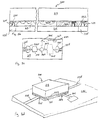
- FIG. 3a shows a first embodiment MMIC 300 in which matching circuitry including transmission lines 302, resistors 304, capacitors 306 and other components are formed on the surface of a GaAs die in which the active devices such as MESFETs 308 and HBTs 310 are formed.
- the airbridges 313 linking for example the source pads of MESFET 308 or the emitter pads of HBT 310 form the thermal link with heatsink 314.
- the input and output to the circuit may be taken by vias 318 to the top side ofthe die in the standard manner.
- FIG. 3b An alternative method of routing the input and output signals is shown in FIG. 3b.
- the circuit is similar to that of FIG. 3a except that input 330 and output pads 332 are connected by vias 334 to the planarized surface corresponding to the top of airbridge 313 and dielectric 322.
- FIG. 3c is a sketch of a view from the bottom of the structure.
- a window 335 is etched in heatsink/groundplane 314.
- the structure 300 may be mounted on a substrate 336 patterned with pads and transmission lines 338 as shown in FIG. 3d.
- Pads 334 can be attached to pads and transmission lines 338 by solder bumps for example. This eliminates the backside processing used to form vias 316 and 318 in FIG. 3a.
- FIG. 3c is a sketch of a view from the bottom of the structure.
- a window 335 is etched in heatsink/groundplane 314.
- the structure 300 may be mounted on a substrate 336 patterned with pads and transmission lines 338
- Bias pad 337 is accessible through window 339 in groundplane 314. Bias pad 337 may be connected by a solder bump for example to bias lead 341 in a manner similar to that used for input and output pads 334.
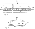
- FIG. 3e Another method of routing the input and output signals from circuit 300 is shown in FIG. 3e.
- Beam leads 340 are bonded or soldered to pads 330 and 332.
- a perspective view of the structure 300 is shown in FIG. 3f.
- This configuration allows the circuit 300 to be utilized as a discrete component in that beam leads 340 may be bonded to pads on printed circuit boards or on alumina substrates, for example.
- This approach is advantageous in that the entire structure 300 can be inexpensively hermetically sealed with a passivating packaging material in much the same way as beam-lead diodes, for example.
- a feature of this embodiment is that the surface of the die that is mounted directly to the heatsink 314 is substantially planar as in the configuration shown in FIG 2.
- the structure of FIG. 3a, 3b, or 3e includes plated airbridges 313 as well as matching circuitry 320 planarized by a low-permittivity, low-loss dielectric layer 322 such as polyimide.
- Shunt components, such as capacitor 306 are easily grounded by etching a via through polyimide 322 prior to flipping and mounting the die on heatsink 314.
- the preferred thickness of the polyimide, and the plated airbridges is between approximately 10 and 20 ⁇ m.
- Heatsink 314 is a high-thermal-conductivity dielectric material such as AlN or BeO, or a gold-plated metal such as copper.
- the dielectric heatsinks can be patterned with evaporated or plated metal to form input/output and bias lines and pads to which the plated features such as via 324 may be connected.
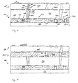
- the transmission lines 302 will not be of the traditional "microstrip" type as shown in FIG. 9a where a lead on top of the substrate in conjunction with the groundplane on the opposite surface of the substrate work to form a transmission medium.
- the transmission line 302 is more in the form of "inverted microstrip", as shown in FIG. 9b, because the high-permittivity die 312 lies above the line 302, rather than between the line 302 and the groundplane 314.
- a true inverted microstrip configuration would have air between the line 302 and the groundplane 314.
- the line and groundplane are separated by the low-permittivity, low-loss dielectric, polyimide, but the design approach is very similar to that of circuits using true inverted microstrip.
- the characteristic impedance of a line is dependent on the ratio of the width of the line 302 to the line's height above the groundplane 314.
- the width to height ratio for a 50-ohm line is approximately unity.
- the ratio is between approximately 0.7 and unity.
- Inverted microstrip has an advantage over standard microstrip in that for a given characteristic impedance, the line 302 will be wider.
- the thickness of the die 312 is not critical in determining the impedance of line 302.
- the die can be left much thicker, e.g. 625 ⁇ m, instead of the 100 or 150 ⁇ m typically required for die thicknesses when using microstrip transmission line.
- a second preferred embodiment shown in FIG. 4 includes a "flipped" MMIC 400 similar to that in FIG. 3a, 3b, or 3e with a MESFET 402, capacitor 404, resistor 406, and transmission line 408 fabricated on the bottom side of die 410, which is then mounted on heatsink 412.
- the bottom side is planarized with a combination of airbridges 414 and polyimide 416.
- Shunt devices, such as capacitor 404 are grounded to heatsink 412 by a via 418 through polyimide 416.
- a second die 420 having a bottom groundplane 422 is bonded to the top surface of die 410. The bonding may be done in a standard manner, e.g.
- the flipped circuit 400 is a high power circuit such as a power amplifier to take advantage of the proximity to heatsink 412, while the upper circuit 424 is one of low power dissipation, e.g. a low-noise amplifier, phase shifter, or digital circuitry.
- Transmission line 408 is instead a modified "stripline" configuration in which a lead is sandwiched between two different dielectric mediums.
- a standard stripline configuration is shown in FIG. 9c.
- the transmission lines are a modified stripline because the central conductor is bounded on one side by a high-permittivity dielectric, e.g. GaAs, and on the other side by a low-permittivity dielectric, e.g. polyimide.
- the design of line 408 to achieve a given characteristic impedance may be considerably different from that of inverted microstrip line 302.
- coplanar waveguide 428 comprised of a signal conductor 430 and two ground lines 432. It should be noted that this feature may be included in any flip-chip configuration, such as that shown in FIG. 3a, 3b, or 3e, for example.
- Coplanar waveguide is advantageous during fabrication of the bottom circuit 400. After the formation of the bottom side circuitry it is desirable to have the capability of testing the circuits. Defective circuits may then be culled before the expense of flipping and mounting the die is incurred. However, the circuits of FIG. 3a, 3b, or 3e, and FIG. 4 which utilize inverted microstrip and suspended stripline respectively are very difficult to test prior to flipping the die. This is because the groundplane, i.e.
- the heatsink 314 and 412 works in conjunction with lines 302 and 408 to form a transmission medium such as inverted microstrip or stripline.
- a transmission medium such as inverted microstrip or stripline.
- the die Prior to flipping the die, the die lacks a groundplane and thus the lines will not have their designed characteristic impedances. This makes the unflipped circuits virtually impossible to test.
- the reference or ground for signal line 430 is provided by coplanar groundlines 432. Therefore, the complete transmission medium is located on the die surface and is independent of the heatsink/groundplane. This allows for testing of the circuitry on circuits 300 and 400 prior to flipping.
- the circuits may be "probed" while still in wafer form, i.e.
- the coplanar waveguide can be functional in the flipped configuration as well by plating the groundlines 432 as is done in forming the airbridge plating 414 to create posts 434 which contact the heatsink 412.
- a transition from the upper circuit 424 is easily made by etching via 426 through die 410 so that contact is made with the center or signal conductor 430 of the coplanar waveguide 428.
- FIG. 10 shows a view from beneath groundplane 412.
- the reference potential, or ground is provided to groundlines 432 by plated posts 434, which contact groundplane 412.
- a window 1000 is etched in groundplane 412 to expose polyimide 1001 and to provide a transition between coplanar waveguide and the inverted microstrip or modified stripline transmission lines 1002 that are used in the input/output and matching circuitry of circuit 400.
- a coaxial structure 436 may be used as a coaxial structure 436.
- Such a structure may be formed by first etching a via hole 438 through dies 420 and 410, filling the vias 438 with a dielectric 440 such as polyimide, etching a hole through the polyimide, and then forming a center conductor 442 by depositing metallization in the hole through the polyimide.
- a coaxial conductor can potentially have superior loss characteristics as compared to a simple plated via.
- FIG. 5 A third preferred embodiment of the invention is shown in FIG. 5. It comprises a lower flip-chip integrated circuit 500 fabricated on a die 502 with matching circuitry and other passive components 503 on the die's top side.
- the top side is planarized with dielectric 504 and a metal groundplane 508 is evaporated and patterned over dielectric 504.
- An upper integrated circuit 506 may then be bonded to the planarized surface as in the structure of FIG. 4
- This approach takes advantage of the fact that the circuit 500 on the bottom side of die 502 does not depend on a particular die thickness for its functionality. Since the die top side can be as far away as 625 ⁇ m or more from the bottom side circuitry, a variety of passive devices, switching, and matching circuitry 503 can be formed on the top side of die 502.
- die 502 can have a power circuit 500 on the bottom side to take advantage of the heatsink 510, and passive circuitry on the die top side. This is in addition to the feature of having a low power dissipating circuit 506 bonded to the planarized surface of circuitry 503.
- contact to the groundplane may be in the form of vias 512 through the polyimide planarizing layer 504.
- circuitry 503 on the top side of die 502 is not limited to passive and matching circuitry.
- epitaxial layers Prior to the fabrication of any circuitry, epitaxial layers may be grown by a method such as molecular beam epitaxy or metal-organic chemical vapor deposition on both the bottom and top sides of the wafer of which die 502 is a constituent. Epitaxy is traditionally performed on only a single surface of a wafer. However, wafers with epitaxy on both sides allows the formation of active devices on both the top and bottom surfaces, thereby further increasing the packing density of the circuitry.
- a fourth embodiment of the invention shown in FIG. 6 is MMIC 600 circuit having clearance on the bottom surface for three dimensional components such as non-planar inductors.
- the airbridge 602 linking the source pads for example of MESFET 604 is in direct contact with heatsink 606.
- a recess is etched in the bottom surface of die 608 in order to form a "tub" 610 approximately 25 to 50 ⁇ m in depth or more. This provides space on the bottom surface of die 608 for components that are too large for the planarization approach of the first three embodiments to accommodate.
- the tub 610 of the structure shown in FIG. 6 can be adapted to accommodate a three-dimensional spiral-wound inductor for example.
- the surface which abuts heatsink 606 is planarized with a dielectric 612 such as polyimide.
- the passive circuitry and components such as inverted microstrip or suspended substrate lines 614, resistors 616, or capacitors 618 can be connected to the active component 604 by metallization 620 which conforms to the step change in the bottom surface of die 608.
- a second integrated circuit 622 may be bonded to the top surface of die 608.
- a fifth preferred embodiment of the invention shown in FIG. 7 is an element 700 in an array of elements forming an active array antenna.
- the element comprises a metal base plate 702 into which an antenna element 704 and cooling duct 706 are mounted.
- the antenna element shown in this embodiment is a dielectrically-loaded type which is fed by wire 708.
- the dielectric 707 which loads the antenna element can be any of a variety of low-low, low-permittivity materials such as quartz, polyimide, Teflon, etc.
- the baseplate 702 also functions as a heatsink for high-power-dissipating circuit 710, which may be for example a power amplifier.
- Airbridge 712 connects source pads of MESFET 714.
- Airbridge 712 is in contact with baseplate 702, which acts as a heatsink for the MESFET. It may also be appreciated that other type of active devices such as HBTs, HEMTs, HFETs, etc. may also benefit from this configuration.
- the top surface of circuit 710 is planarized by depositing dielectric 716 to cover the non-plated regions of the circuit, i.e. areas other than airbridges and ground contacts. Resistors 718, capacitors 720, and transmission lines in the form of stripline 722 may be formed on the surface of die 724.
- the output of the high-power circuit is taken from pad 726 on the surface of the semiconductor die to antenna feed wire 708.
- An advantage of using the flip-chip approach with top-side matching circuitry and transmission lines is that the line length from the amplifier output 726 to the antenna is minimal. This is important in ensuring that the highest power output possible is provided to the antenna element.
- Active arrays typically have long feed lines between the power amplifier and the antenna element. Such arrays are comparatively inefficient because of the losses involved in transmitting the signal from the amplifier to the antenna.
- a second circuit may be mounted on the bottom side of die 724
- a phase shifter circuit 726 is shown.
- the phase shifter integrated circuit is shown with a groundplane 728 and is bonded directly to die 724 with an adhesive such as thermoplastic or epoxy.
- Connections between the power amplifier 710 and the phase shifter circuit 726 are in the form of plated vias 730 through dies 724 and 732.
- the phase shifter 726 may comprise MESFETs 734 as shown, PIN diodes, transmission lines, resistors, and capacitors, etc.
- the surface of circuit 726 is planarized with a low-permittivity, low-loss dielectric 736 such as polyimide or a like material.
- Transmission lines may be in the form of coplanar waveguide 738 having a central signal line between ground lines or as suspended stripline or inverted microstrip.
- a DC/RF/Control logic distribution printed circuit board 740 is mounted on the planarized surface of phase shifter circuit 726.
- Such a board can take logic inputs from an antenna control computer, or low amplitude RF signals from pre-amplifier circuitry.
- the board's function could be to provide phase selection information to the phase shifter such that the signal from the antenna element 704 works in conjunction with other elements mounted in baseplate 702 (see FIG. 8) to produce an electronically steerable antenna beam.
- the system described in this embodiment might find application in a variety of applications, from microwave distribution networks to radars.
- Internal and external connections can be ohmic, capacitive, inductive, direct or indirect, via intervening circuits or otherwise. Implementation is contemplated in discrete components or fully integrated circuits in silicon, gallium arsenide, or other electronic materials families, as well as in optical-based or other technology-based forms and embodiments.
Landscapes
- Semiconductor Integrated Circuits (AREA)
- Cooling Or The Like Of Semiconductors Or Solid State Devices (AREA)
- Bipolar Integrated Circuits (AREA)
Applications Claiming Priority (2)
| Application Number | Priority Date | Filing Date | Title |
|---|---|---|---|
| US298822 | 1994-08-31 | ||
| US08/298,822 US5521406A (en) | 1994-08-31 | 1994-08-31 | Integrated circuit with improved thermal impedance |
Publications (3)
| Publication Number | Publication Date |
|---|---|
| EP0703614A2 true EP0703614A2 (de) | 1996-03-27 |
| EP0703614A3 EP0703614A3 (de) | 1997-03-12 |
| EP0703614B1 EP0703614B1 (de) | 2006-10-04 |
Family
ID=23152138
Family Applications (1)
| Application Number | Title | Priority Date | Filing Date |
|---|---|---|---|
| EP95113448A Expired - Lifetime EP0703614B1 (de) | 1994-08-31 | 1995-08-28 | Flip-Chip mit wärmeleitender Schicht |
Country Status (4)
| Country | Link |
|---|---|
| US (5) | US5521406A (de) |
| EP (1) | EP0703614B1 (de) |
| JP (1) | JP4231111B2 (de) |
| DE (1) | DE69535250T2 (de) |
Cited By (5)
| Publication number | Priority date | Publication date | Assignee | Title |
|---|---|---|---|---|
| EP0741414A3 (de) * | 1995-04-27 | 1998-10-21 | Hughes Aircraft Company | Integrierte monolithische Mikrowellenschaltung und Verfahren |
| EP0920067A3 (de) * | 1997-11-12 | 2001-05-16 | Com Dev Ltd. | Mikrowellenschalter und Verfahren zu dessen Betrieb |
| GB2371404A (en) * | 2001-01-23 | 2002-07-24 | Univ Glasgow | An optical device with a heat sink |
| GB2392011A (en) * | 2002-06-19 | 2004-02-18 | Intel Corp | Bridges for microelectromechanical structures |
| CN113594658A (zh) * | 2021-08-11 | 2021-11-02 | 上海交通大学 | 接地共面波导到悬置微带线的宽带过渡结构 |
Families Citing this family (109)
| Publication number | Priority date | Publication date | Assignee | Title |
|---|---|---|---|---|
| DE4410947C1 (de) * | 1994-03-29 | 1995-06-01 | Siemens Ag | Halbleiterbauelement für vertikale Integration und Herstellungsverfahren |
| US5521406A (en) * | 1994-08-31 | 1996-05-28 | Texas Instruments Incorporated | Integrated circuit with improved thermal impedance |
| GB2297651B (en) * | 1995-02-03 | 1999-05-26 | Gec Marconi Avionics Holdings | Electrical apparatus |
| US5942791A (en) * | 1996-03-06 | 1999-08-24 | Gec-Marconi Limited | Micromachined devices having microbridge structure |
| US5949144A (en) * | 1996-05-20 | 1999-09-07 | Harris Corporation | Pre-bond cavity air bridge |
| US5679979A (en) * | 1996-05-21 | 1997-10-21 | Weingand; Christopher Dirk | Surface mount package with heat transfer feature |
| US5939739A (en) * | 1996-05-31 | 1999-08-17 | The Whitaker Corporation | Separation of thermal and electrical paths in flip chip ballasted power heterojunction bipolar transistors |
| US7774230B2 (en) | 1996-06-10 | 2010-08-10 | Phoenix Licensing, Llc | System, method, and computer program product for selecting and presenting financial products and services |
| US6999938B1 (en) | 1996-06-10 | 2006-02-14 | Libman Richard M | Automated reply generation direct marketing system |
| US5883422A (en) * | 1996-06-28 | 1999-03-16 | The Whitaker Corporation | Reduced parasitic capacitance semiconductor devices |
| US6310394B1 (en) | 1996-06-28 | 2001-10-30 | Tyco Electronics | Reduced parasitic capacitance semiconductor devices |
| JP3185918B2 (ja) * | 1996-08-05 | 2001-07-11 | 株式会社村田製作所 | 電子装置 |
| SE508139C2 (sv) * | 1996-12-20 | 1998-08-31 | Ericsson Telefon Ab L M | Metod och anordning för anslutning av elektrisk komponent till kretskort |
| JP3119191B2 (ja) * | 1997-02-27 | 2000-12-18 | 株式会社村田製作所 | 平面誘電体集積回路 |
| US20050027601A1 (en) * | 1998-12-22 | 2005-02-03 | Walker Jay S. | Products and processes for vending a plurality of products |
| US20060122881A1 (en) * | 1997-03-21 | 2006-06-08 | Walker Jay S | Systems and methods for vending promotions |
| EP0887879A1 (de) * | 1997-06-23 | 1998-12-30 | Nec Corporation | Phasengesteuerte Antennenvorrichtung |
| US5841184A (en) * | 1997-09-19 | 1998-11-24 | The Whitaker Corporation | Integrated emitter drain bypass capacitor for microwave/RF power device applications |
| US5945734A (en) * | 1997-09-19 | 1999-08-31 | Samsung Electronics Co., Ltd. | Wire-bond free input/output interface for GaAs ICs with means of determining known good die |
| US6037822A (en) * | 1997-09-30 | 2000-03-14 | Intel Corporation | Method and apparatus for distributing a clock on the silicon backside of an integrated circuit |
| AU1064899A (en) * | 1997-10-03 | 1999-04-27 | Board Of Trustees Of The University Of Arkansas, The | Methods of making flexible substrates for electronic packaging and flexible substrates formed by the method |
| US7894936B2 (en) * | 1997-10-09 | 2011-02-22 | Walker Digital, Llc | Products and processes for managing the prices of vending machine inventory |
| US6198168B1 (en) * | 1998-01-20 | 2001-03-06 | Micron Technologies, Inc. | Integrated circuits using high aspect ratio vias through a semiconductor wafer and method for forming same |
| JP3013831B2 (ja) * | 1998-01-26 | 2000-02-28 | 日本電気株式会社 | Mmicパッケージ |
| US6090636A (en) * | 1998-02-26 | 2000-07-18 | Micron Technology, Inc. | Integrated circuits using optical waveguide interconnects formed through a semiconductor wafer and methods for forming same |
| US6150188A (en) | 1998-02-26 | 2000-11-21 | Micron Technology Inc. | Integrated circuits using optical fiber interconnects formed through a semiconductor wafer and methods for forming same |
| US5990757A (en) * | 1998-06-05 | 1999-11-23 | Raytheon Company | Gallium arsenide monolithic microwave integrated circuits employing thermally bumped devices |
| US6081037A (en) * | 1998-06-22 | 2000-06-27 | Motorola, Inc. | Semiconductor component having a semiconductor chip mounted to a chip mount |
| US6586835B1 (en) | 1998-08-31 | 2003-07-01 | Micron Technology, Inc. | Compact system module with built-in thermoelectric cooling |
| US6281042B1 (en) | 1998-08-31 | 2001-08-28 | Micron Technology, Inc. | Structure and method for a high performance electronic packaging assembly |
| US6219237B1 (en) | 1998-08-31 | 2001-04-17 | Micron Technology, Inc. | Structure and method for an electronic assembly |
| US6392296B1 (en) | 1998-08-31 | 2002-05-21 | Micron Technology, Inc. | Silicon interposer with optical connections |
| FR2785448B1 (fr) * | 1998-10-30 | 2001-01-26 | Alstom Technology | Procede de fabrication d'une electrode de commande de grille pour transistor igbt |
| US6118177A (en) * | 1998-11-17 | 2000-09-12 | Lucent Technologies, Inc. | Heatspreader for a flip chip device, and method for connecting the heatspreader |
| US6122187A (en) * | 1998-11-23 | 2000-09-19 | Micron Technology, Inc. | Stacked integrated circuits |
| US6303423B1 (en) * | 1998-12-21 | 2001-10-16 | Megic Corporation | Method for forming high performance system-on-chip using post passivation process |
| SE515661C2 (sv) * | 1998-12-22 | 2001-09-17 | Ericsson Telefon Ab L M | Trådbondningskompensering |
| US7826923B2 (en) | 1998-12-22 | 2010-11-02 | Walker Digital, Llc | Products and processes for vending a plurality of products |
| JP3481481B2 (ja) * | 1998-12-24 | 2003-12-22 | 日本電気株式会社 | フェーズドアレイアンテナおよびその製造方法 |
| US6373447B1 (en) * | 1998-12-28 | 2002-04-16 | Kawasaki Steel Corporation | On-chip antenna, and systems utilizing same |
| JP2000216343A (ja) * | 1999-01-27 | 2000-08-04 | Nec Corp | 半導体集積回路 |
| US6255852B1 (en) | 1999-02-09 | 2001-07-03 | Micron Technology, Inc. | Current mode signal interconnects and CMOS amplifier |
| US6208225B1 (en) | 1999-02-25 | 2001-03-27 | Formfactor, Inc. | Filter structures for integrated circuit interfaces |
| US6218910B1 (en) * | 1999-02-25 | 2001-04-17 | Formfactor, Inc. | High bandwidth passive integrated circuit tester probe card assembly |
| US6459343B1 (en) | 1999-02-25 | 2002-10-01 | Formfactor, Inc. | Integrated circuit interconnect system forming a multi-pole filter |
| US6448865B1 (en) | 1999-02-25 | 2002-09-10 | Formfactor, Inc. | Integrated circuit interconnect system |
| US6180995B1 (en) * | 1999-05-06 | 2001-01-30 | Spectrian Corporation | Integrated passive devices with reduced parasitic substrate capacitance |
| US6329280B1 (en) | 1999-05-13 | 2001-12-11 | International Business Machines Corporation | Interim oxidation of silsesquioxane dielectric for dual damascene process |
| US6434726B1 (en) | 1999-06-29 | 2002-08-13 | Lucent Technologies Inc. | System and method of transmission using coplanar bond wires |
| US7554829B2 (en) | 1999-07-30 | 2009-06-30 | Micron Technology, Inc. | Transmission lines for CMOS integrated circuits |
| US6507110B1 (en) | 2000-03-08 | 2003-01-14 | Teledyne Technologies Incorporated | Microwave device and method for making same |
| US6316981B1 (en) * | 2000-03-13 | 2001-11-13 | Intel Corporation | Signal distribution network on backside of substrate |
| US6180445B1 (en) * | 2000-04-24 | 2001-01-30 | Taiwan Semiconductor Manufacturing Company | Method to fabricate high Q inductor by redistribution layer when flip-chip package is employed |
| US6368929B1 (en) * | 2000-08-17 | 2002-04-09 | Motorola, Inc. | Method of manufacturing a semiconductor component and semiconductor component thereof |
| US7218991B2 (en) * | 2000-08-22 | 2007-05-15 | Walker Digital, Llc | System for vending physical and information items |
| JP3462166B2 (ja) * | 2000-09-08 | 2003-11-05 | 富士通カンタムデバイス株式会社 | 化合物半導体装置 |
| WO2002043145A1 (en) * | 2000-11-27 | 2002-05-30 | Ultrarf, Inc. | Integrated passive devices with reduced parasitic substrate capacitance |
| EP1265466A3 (de) * | 2001-06-05 | 2004-07-21 | Dai Nippon Printing Co., Ltd. | Verfahren zur Herstellung einer Leiterplatte mit passiven Elementen und Leiterplatte mit passiven Elementen |
| US6670865B2 (en) * | 2001-06-06 | 2003-12-30 | Noel A. Lopez | Method and apparatus for low loss high frequency transmission |
| CN1579018A (zh) * | 2001-08-29 | 2005-02-09 | 皇家飞利浦电子股份有限公司 | 具有凸起桥的集成电路器件及其制造方法 |
| US6514783B1 (en) * | 2001-09-17 | 2003-02-04 | Applied Micro Circuits Corporation | Method for determining a layout for a flip-chip transition interface structure |
| US6639322B1 (en) * | 2001-09-17 | 2003-10-28 | Applied Micro Circuits Corporation | Flip-chip transition interface structure |
| JP3973402B2 (ja) * | 2001-10-25 | 2007-09-12 | 株式会社日立製作所 | 高周波回路モジュール |
| JP3674780B2 (ja) * | 2001-11-29 | 2005-07-20 | ユーディナデバイス株式会社 | 高周波半導体装置 |
| US7101770B2 (en) | 2002-01-30 | 2006-09-05 | Micron Technology, Inc. | Capacitive techniques to reduce noise in high speed interconnections |
| US6686819B2 (en) * | 2002-02-01 | 2004-02-03 | Intel Corporation | Dual referenced microstrip |
| US7235457B2 (en) | 2002-03-13 | 2007-06-26 | Micron Technology, Inc. | High permeability layered films to reduce noise in high speed interconnects |
| US6949992B2 (en) * | 2002-03-20 | 2005-09-27 | Powerwave Technologies, Inc. | System and method of providing highly isolated radio frequency interconnections |
| US6933603B2 (en) * | 2002-07-11 | 2005-08-23 | Teledyne Technologies Incorporated | Multi-substrate layer semiconductor packages and method for making same |
| US20050027622A1 (en) * | 2003-07-30 | 2005-02-03 | Walker Jay S. | Products and processes for vending a plurality of products via defined groups |
| JP2005093867A (ja) * | 2003-09-19 | 2005-04-07 | Seiko Epson Corp | 半導体装置及びその製造方法 |
| US20060035413A1 (en) * | 2004-01-13 | 2006-02-16 | Cookson Electronics, Inc. | Thermal protection for electronic components during processing |
| US20050151555A1 (en) * | 2004-01-13 | 2005-07-14 | Cookson Electronics, Inc. | Cooling devices and methods of using them |
| FR2867609B1 (fr) * | 2004-03-12 | 2006-12-01 | United Monolithic Semiconduct | Boitier miniature hyperfrequence de puissance et procede de fabrication du boitier |
| US7112882B2 (en) * | 2004-08-25 | 2006-09-26 | Taiwan Semiconductor Manufacturing Co., Ltd. | Structures and methods for heat dissipation of semiconductor integrated circuits |
| US7138300B2 (en) * | 2004-09-22 | 2006-11-21 | Taiwan Semiconductor Manufacturing Co., Ltd. | Structural design for flip-chip assembly |
| DE102004059884A1 (de) * | 2004-12-10 | 2006-06-29 | Forschungsverbund Berlin E.V. | Verfahren zur Flip-Chip-Montage von Mikrochips und damit hergestellte elektronische Baugruppe |
| FR2879830B1 (fr) * | 2004-12-20 | 2007-03-02 | United Monolithic Semiconduct | Composant electronique miniature pour applications hyperfrequences |
| JP2006222609A (ja) * | 2005-02-09 | 2006-08-24 | Sony Corp | 高周波信号伝送回路の製造方法及び高周波信号伝送回路装置 |
| US7348597B1 (en) * | 2005-03-14 | 2008-03-25 | Xilinx, Inc. | Apparatus for performing high frequency electronic package testing |
| US8384189B2 (en) * | 2005-03-29 | 2013-02-26 | Megica Corporation | High performance system-on-chip using post passivation process |
| US9252067B1 (en) | 2006-01-25 | 2016-02-02 | Lockheed Martin Corporation | Hybrid microwave integrated circuit |
| US7391067B1 (en) * | 2006-01-25 | 2008-06-24 | Lockheed Martin Corporation | Hybrid microwave integrated circuit |
| US7474005B2 (en) * | 2006-05-31 | 2009-01-06 | Alcatel-Lucent Usa Inc. | Microelectronic element chips |
| US8067840B2 (en) * | 2006-06-20 | 2011-11-29 | Nxp B.V. | Power amplifier assembly |
| JP4433097B2 (ja) * | 2007-04-27 | 2010-03-17 | 株式会社村田製作所 | 無線icデバイス |
| US7656236B2 (en) | 2007-05-15 | 2010-02-02 | Teledyne Wireless, Llc | Noise canceling technique for frequency synthesizer |
| JP5104131B2 (ja) * | 2007-08-31 | 2012-12-19 | 富士通セミコンダクター株式会社 | 無線装置および無線装置が備えるアンテナ |
| US8143654B1 (en) * | 2008-01-16 | 2012-03-27 | Triquint Semiconductor, Inc. | Monolithic microwave integrated circuit with diamond layer |
| US8138027B2 (en) | 2008-03-07 | 2012-03-20 | Stats Chippac, Ltd. | Optical semiconductor device having pre-molded leadframe with window and method therefor |
| US8028406B2 (en) * | 2008-04-03 | 2011-10-04 | International Business Machines Corporation | Methods of fabricating coplanar waveguide structures |
| US8179045B2 (en) * | 2008-04-22 | 2012-05-15 | Teledyne Wireless, Llc | Slow wave structure having offset projections comprised of a metal-dielectric composite stack |
| US8339790B2 (en) * | 2010-09-10 | 2012-12-25 | Raytheon Company | Monolithic microwave integrated circuit |
| US9024408B2 (en) * | 2010-12-29 | 2015-05-05 | Stmicroelectronics, Inc. | Double side wafer process, method and device |
| JP2013021001A (ja) * | 2011-07-07 | 2013-01-31 | Renesas Electronics Corp | 半導体装置及び半導体装置の製造方法 |
| US9679869B2 (en) | 2011-09-02 | 2017-06-13 | Skyworks Solutions, Inc. | Transmission line for high performance radio frequency applications |
| US20140168010A1 (en) * | 2011-12-22 | 2014-06-19 | Farrokh Mohamadi | Extended range, high data rate, point-to-point crosslink placed on fixed or mobile elevated platforms |
| EP3401997B1 (de) * | 2011-12-22 | 2022-08-24 | Nokia Technologies Oy | Vorrichtung, bestehend aus einer antenne und einer grundplatte und verfahren zur herstellung |
| US8912634B2 (en) * | 2012-03-29 | 2014-12-16 | International Business Machines Corporation | High frequency transition matching in an electronic package for millimeter wave semiconductor dies |
| KR102250612B1 (ko) | 2012-06-14 | 2021-05-10 | 스카이워크스 솔루션즈, 인코포레이티드 | 고조파 종단 회로를 포함하는 전력 증폭기 모듈 및 관련된 시스템, 장치, 및 방법 |
| US9041206B2 (en) * | 2013-03-12 | 2015-05-26 | Taiwan Semiconductor Manufacturing Company, Ltd. | Interconnect structure and method |
| US9202660B2 (en) | 2013-03-13 | 2015-12-01 | Teledyne Wireless, Llc | Asymmetrical slow wave structures to eliminate backward wave oscillations in wideband traveling wave tubes |
| JP6005204B1 (ja) * | 2015-03-30 | 2016-10-12 | 日本写真印刷株式会社 | 薄膜トランジスタの製造方法、および薄膜トランジスタ |
| US10354980B1 (en) | 2018-03-22 | 2019-07-16 | Sandisk Technologies Llc | Three-dimensional memory device containing bonded chip assembly with through-substrate via structures and method of making the same |
| US10354987B1 (en) * | 2018-03-22 | 2019-07-16 | Sandisk Technologies Llc | Three-dimensional memory device containing bonded chip assembly with through-substrate via structures and method of making the same |
| US12021033B2 (en) * | 2020-05-15 | 2024-06-25 | Taiwan Semiconductor Manufacturing Ltd. | Integrated circuit device having active region coupled to metal layers on opposite sides of substrate, and method |
| US11533024B2 (en) | 2020-06-25 | 2022-12-20 | Wolfspeed, Inc. | Multi-zone radio frequency transistor amplifiers |
| US12531524B2 (en) | 2020-06-25 | 2026-01-20 | Macom Technology Solutions Holdings, Inc. | Multi-zone radio frequency transistor amplifiers |
| US12406949B2 (en) * | 2021-08-04 | 2025-09-02 | Nxp Usa, Inc. | Semiconductor device with RF interposer and method therefor |
Family Cites Families (16)
| Publication number | Priority date | Publication date | Assignee | Title |
|---|---|---|---|---|
| US3534376A (en) * | 1968-01-30 | 1970-10-13 | Webb James E | High impact antenna |
| JPS5843578A (ja) * | 1981-09-08 | 1983-03-14 | Mitsubishi Electric Corp | GaAs集積回路 |
| JPS6271256A (ja) * | 1985-09-25 | 1987-04-01 | Toshiba Corp | 化合物半導体集積回路 |
| JPH0618197B2 (ja) * | 1987-07-30 | 1994-03-09 | 日本電気株式会社 | 超伝導モノリシックマイクロ波集積回路 |
| US4959705A (en) * | 1988-10-17 | 1990-09-25 | Ford Microelectronics, Inc. | Three metal personalization of application specific monolithic microwave integrated circuit |
| US4992764A (en) * | 1989-02-21 | 1991-02-12 | Hittite Microwave Corporation | High-power FET circuit |
| US5319237A (en) * | 1990-03-09 | 1994-06-07 | Thomson Composants Microondes | Power semiconductor component |
| US5202752A (en) * | 1990-05-16 | 1993-04-13 | Nec Corporation | Monolithic integrated circuit device |
| US5057908A (en) * | 1990-07-10 | 1991-10-15 | Iowa State University Research Foundation, Inc. | High power semiconductor device with integral heat sink |
| JPH0590801A (ja) * | 1991-09-27 | 1993-04-09 | Nec Corp | マイクロ波集積回路 |
| JPH05129345A (ja) * | 1991-11-08 | 1993-05-25 | Toshiba Corp | マイクロ波集積回路の製造方法 |
| US5268315A (en) * | 1992-09-04 | 1993-12-07 | Tektronix, Inc. | Implant-free heterojunction bioplar transistor integrated circuit process |
| JP3084541B2 (ja) * | 1992-09-18 | 2000-09-04 | シャープ株式会社 | 縦型構造トランジスタ |
| JPH06125208A (ja) * | 1992-10-09 | 1994-05-06 | Mitsubishi Electric Corp | マイクロ波集積回路およびその製造方法 |
| US6028348A (en) * | 1993-11-30 | 2000-02-22 | Texas Instruments Incorporated | Low thermal impedance integrated circuit |
| US5521406A (en) * | 1994-08-31 | 1996-05-28 | Texas Instruments Incorporated | Integrated circuit with improved thermal impedance |
-
1994
- 1994-08-31 US US08/298,822 patent/US5521406A/en not_active Expired - Lifetime
- 1994-11-14 US US08/339,429 patent/US5532506A/en not_active Expired - Lifetime
-
1995
- 1995-06-07 US US08/473,621 patent/US5612257A/en not_active Expired - Lifetime
- 1995-06-07 US US08/477,717 patent/US5614442A/en not_active Expired - Lifetime
- 1995-08-28 EP EP95113448A patent/EP0703614B1/de not_active Expired - Lifetime
- 1995-08-28 DE DE69535250T patent/DE69535250T2/de not_active Expired - Lifetime
- 1995-08-31 JP JP22401395A patent/JP4231111B2/ja not_active Expired - Fee Related
-
1996
- 1996-07-16 US US08/680,892 patent/US5717231A/en not_active Expired - Lifetime
Non-Patent Citations (1)
| Title |
|---|
| None |
Cited By (11)
| Publication number | Priority date | Publication date | Assignee | Title |
|---|---|---|---|---|
| EP0741414A3 (de) * | 1995-04-27 | 1998-10-21 | Hughes Aircraft Company | Integrierte monolithische Mikrowellenschaltung und Verfahren |
| EP0920067A3 (de) * | 1997-11-12 | 2001-05-16 | Com Dev Ltd. | Mikrowellenschalter und Verfahren zu dessen Betrieb |
| GB2371404A (en) * | 2001-01-23 | 2002-07-24 | Univ Glasgow | An optical device with a heat sink |
| GB2371404B (en) * | 2001-01-23 | 2003-07-09 | Univ Glasgow | Improvements in or relating to optical devices |
| GB2392011A (en) * | 2002-06-19 | 2004-02-18 | Intel Corp | Bridges for microelectromechanical structures |
| US6812810B2 (en) | 2002-06-19 | 2004-11-02 | Intel Corporation | Bridges for microelectromechanical structures |
| GB2422720A (en) * | 2002-06-19 | 2006-08-02 | Intel Corp | Bridges for microelectromechanical structures |
| GB2392011B (en) * | 2002-06-19 | 2006-08-23 | Intel Corp | Bridges for microelectromechanical structures |
| GB2422720B (en) * | 2002-06-19 | 2006-12-20 | Intel Corp | Bridges for microelectromechanical structures |
| CN113594658A (zh) * | 2021-08-11 | 2021-11-02 | 上海交通大学 | 接地共面波导到悬置微带线的宽带过渡结构 |
| CN113594658B (zh) * | 2021-08-11 | 2022-04-08 | 上海交通大学 | 接地共面波导到悬置微带线的宽带过渡结构 |
Also Published As
| Publication number | Publication date |
|---|---|
| EP0703614B1 (de) | 2006-10-04 |
| DE69535250D1 (de) | 2006-11-16 |
| US5717231A (en) | 1998-02-10 |
| DE69535250T2 (de) | 2007-08-23 |
| US5612257A (en) | 1997-03-18 |
| JPH08213474A (ja) | 1996-08-20 |
| US5521406A (en) | 1996-05-28 |
| JP4231111B2 (ja) | 2009-02-25 |
| US5532506A (en) | 1996-07-02 |
| US5614442A (en) | 1997-03-25 |
| EP0703614A3 (de) | 1997-03-12 |
Similar Documents
| Publication | Publication Date | Title |
|---|---|---|
| US5612257A (en) | Method of making flip-chip microwave integrated circuit | |
| US5206712A (en) | Building block approach to microwave modules | |
| EP0782766B1 (de) | Mikrowellen-/millimeterwellen-schaltungsstruktur mit einzeln montierten elementen vom flipchiptyp und herstellungsverfahren dafür | |
| Heinrich | The flip-chip approach for millimeter wave packaging | |
| EP0595346B1 (de) | Modulare Mikrowellen-Anordnungseinheit und ihre Verbindungsstruktur | |
| US5637922A (en) | Wireless radio frequency power semiconductor devices using high density interconnect | |
| US5583468A (en) | High frequency transition from a microstrip transmission line to an MMIC coplanar waveguide | |
| US5347086A (en) | Coaxial die and substrate bumps | |
| JP3487639B2 (ja) | 半導体装置 | |
| US6329702B1 (en) | High frequency carrier | |
| US20210313283A1 (en) | Multi level radio frequency (rf) integrated circuit components including passive devices | |
| JP3275851B2 (ja) | 高周波集積回路 | |
| JP2790033B2 (ja) | 半導体装置 | |
| US6507110B1 (en) | Microwave device and method for making same | |
| Carrillo-Ramirez et al. | A highly integrated millimeter-wave active antenna array using BCB and silicon substrate | |
| US6998292B2 (en) | Apparatus and method for inter-chip or chip-to-substrate connection with a sub-carrier | |
| US4996588A (en) | Device for interconnection and protection of a bare microwave component chip | |
| US6933603B2 (en) | Multi-substrate layer semiconductor packages and method for making same | |
| US9520368B1 (en) | Integrated circuit system having stripline structure | |
| JPH09283693A (ja) | 高周波半導体装置 | |
| Watanabe et al. | HEMT millimeter-wave monolithic IC technology for 76-GHz automotive radar | |
| JP3441974B2 (ja) | 半導体装置の構造及び製造方法 | |
| JP3992862B2 (ja) | 高周波マルチチップモジュール | |
| Budka et al. | Embedded transmission line MMIC 1-W flip chip assembly using a Z-axis interconnect | |
| JPH0427170Y2 (de) |
Legal Events
| Date | Code | Title | Description |
|---|---|---|---|
| PUAI | Public reference made under article 153(3) epc to a published international application that has entered the european phase |
Free format text: ORIGINAL CODE: 0009012 |
|
| AK | Designated contracting states |
Kind code of ref document: A2 Designated state(s): DE FR GB IT NL |
|
| PUAL | Search report despatched |
Free format text: ORIGINAL CODE: 0009013 |
|
| AK | Designated contracting states |
Kind code of ref document: A3 Designated state(s): DE FR GB IT NL |
|
| 17P | Request for examination filed |
Effective date: 19970912 |
|
| 17Q | First examination report despatched |
Effective date: 19990930 |
|
| GRAP | Despatch of communication of intention to grant a patent |
Free format text: ORIGINAL CODE: EPIDOSNIGR1 |
|
| GRAS | Grant fee paid |
Free format text: ORIGINAL CODE: EPIDOSNIGR3 |
|
| GRAA | (expected) grant |
Free format text: ORIGINAL CODE: 0009210 |
|
| AK | Designated contracting states |
Kind code of ref document: B1 Designated state(s): DE FR GB IT NL |
|
| PG25 | Lapsed in a contracting state [announced via postgrant information from national office to epo] |
Ref country code: NL Free format text: LAPSE BECAUSE OF FAILURE TO SUBMIT A TRANSLATION OF THE DESCRIPTION OR TO PAY THE FEE WITHIN THE PRESCRIBED TIME-LIMIT Effective date: 20061004 Ref country code: IT Free format text: LAPSE BECAUSE OF FAILURE TO SUBMIT A TRANSLATION OF THE DESCRIPTION OR TO PAY THE FEE WITHIN THE PRE;WARNING: LAPSES OF ITALIAN PATENTS WITH EFFECTIVE DATE BEFORE 2007 MAY HAVE OCCURRED AT ANY TIME BEFORE 2007. THE CORRECT EFFECTIVE DATE MAY BE DIFFERENT FROM THE ONE RECORDED.SCRIBED TIME-LIMIT Effective date: 20061004 |
|
| REG | Reference to a national code |
Ref country code: GB Ref legal event code: FG4D |
|
| REF | Corresponds to: |
Ref document number: 69535250 Country of ref document: DE Date of ref document: 20061116 Kind code of ref document: P |
|
| NLV1 | Nl: lapsed or annulled due to failure to fulfill the requirements of art. 29p and 29m of the patents act | ||
| ET | Fr: translation filed | ||
| PLBE | No opposition filed within time limit |
Free format text: ORIGINAL CODE: 0009261 |
|
| STAA | Information on the status of an ep patent application or granted ep patent |
Free format text: STATUS: NO OPPOSITION FILED WITHIN TIME LIMIT |
|
| 26N | No opposition filed |
Effective date: 20070705 |
|
| PGFP | Annual fee paid to national office [announced via postgrant information from national office to epo] |
Ref country code: FR Payment date: 20090806 Year of fee payment: 15 |
|
| PGFP | Annual fee paid to national office [announced via postgrant information from national office to epo] |
Ref country code: DE Payment date: 20100831 Year of fee payment: 16 |
|
| PGFP | Annual fee paid to national office [announced via postgrant information from national office to epo] |
Ref country code: GB Payment date: 20100708 Year of fee payment: 16 |
|
| REG | Reference to a national code |
Ref country code: FR Ref legal event code: ST Effective date: 20110502 |
|
| PG25 | Lapsed in a contracting state [announced via postgrant information from national office to epo] |
Ref country code: FR Free format text: LAPSE BECAUSE OF NON-PAYMENT OF DUE FEES Effective date: 20100831 |
|
| GBPC | Gb: european patent ceased through non-payment of renewal fee |
Effective date: 20110828 |
|
| REG | Reference to a national code |
Ref country code: DE Ref legal event code: R119 Ref document number: 69535250 Country of ref document: DE Effective date: 20120301 |
|
| PG25 | Lapsed in a contracting state [announced via postgrant information from national office to epo] |
Ref country code: GB Free format text: LAPSE BECAUSE OF NON-PAYMENT OF DUE FEES Effective date: 20110828 |
|
| PG25 | Lapsed in a contracting state [announced via postgrant information from national office to epo] |
Ref country code: DE Free format text: LAPSE BECAUSE OF NON-PAYMENT OF DUE FEES Effective date: 20120301 |