EP0703620B1 - Schaltung zur Verhinderung der Zündung von parasitären Bauelementen in integrierten Schaltungen bestehend aus einer Leistungsstufe und einer Niederspannungssteuerschaltung - Google Patents
Schaltung zur Verhinderung der Zündung von parasitären Bauelementen in integrierten Schaltungen bestehend aus einer Leistungsstufe und einer Niederspannungssteuerschaltung Download PDFInfo
- Publication number
- EP0703620B1 EP0703620B1 EP94830444A EP94830444A EP0703620B1 EP 0703620 B1 EP0703620 B1 EP 0703620B1 EP 94830444 A EP94830444 A EP 94830444A EP 94830444 A EP94830444 A EP 94830444A EP 0703620 B1 EP0703620 B1 EP 0703620B1
- Authority
- EP
- European Patent Office
- Prior art keywords
- region
- circuit
- voltage
- transistor
- reference potential
- Prior art date
- Legal status (The legal status is an assumption and is not a legal conclusion. Google has not performed a legal analysis and makes no representation as to the accuracy of the status listed.)
- Expired - Lifetime
Links
Images

Classifications
-
- H—ELECTRICITY
- H10—SEMICONDUCTOR DEVICES; ELECTRIC SOLID-STATE DEVICES NOT OTHERWISE PROVIDED FOR
- H10D—INORGANIC ELECTRIC SEMICONDUCTOR DEVICES
- H10D89/00—Aspects of integrated devices not covered by groups H10D84/00 - H10D88/00
- H10D89/60—Integrated devices comprising arrangements for electrical or thermal protection, e.g. protection circuits against electrostatic discharge [ESD]
Definitions
- the present invention relates to a circuit for preventing turn-on of parasitic components in integrated circuits including a power stage and low-voltage control circuitry.
- a power stage e.g. MOSFET power transistor, VDMOS
- the relative low-voltage drive circuits e.g. comprising NMOS and PMOS transistors.
- the drive voltage of such devices may oscillate between two fairly high values (a few tens of volts) symmetrical with respect to the reference voltage (ground), in which case the problem arises of maintaining the drive circuit components and the power stage isolated.
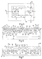
- FIG. 1 showing an integrated device 1 comprising a power transistor (VDMOS) 2 and relative control circuitry (drive stage) 3.
- VDMOS power transistor
- the drain terminal D of VDMOS 2 presents voltage V D
- its source terminal S is grounded
- its gate terminal G is driven by drive stage 3
- 4 indicates the relative parasitic diode.
- power transistor 2 presents N + -type source and drain regions.
- the drive stage are shown only an input terminal 5 supplied with input voltage V IN (oscillating drive voltage); an N + -type region 6 connected to input terminal 5 (and forming part of any component, e.g.
- Figure 1 also shows two parasitic NPN transistors 8, 9 and a parasitic PNP transistor 10, which are associated with the Figure 1 structure as shown more clearly in the example implementation in Figure 2.
- Figure 2 shows a cross section of a silicon wafer including an N + -type substrate 11, and an N - -type epitaxial layer 12 forming with substrate 11 the drain region of VDMOS 2.
- VDMOS 2 including N + -type source regions 15, polysilicon gate regions 16 embedded in insulating layer 17, and metal source line 18.
- CMOS component including in known manner an N-channel and a P-channel MOS transistor
- P + -type regions 22, 23 provide for isolating the various components.
- region 22 encloses and isolates the low-voltage components, corresponds to region 7 in Figure 1, and separates an N-well layer 24 and a P-well layer 25 over buried layer 20.
- N-well layer 24 presents an N + -type region 29; and P + -type regions 26 constituting the drain and source of the PMOS transistor and located beneath gate region 27 embedded in dielectric layer 28.
- P-well layer 25 presents N + -type regions 30 constituting the drain and source of the NMOS transistor and located beneath gate region 31 embedded in dielectric layer 32.
- Metal lines 33 contact the NMOS and PMOS transistor regions in the usual way.
- the N + -type regions form parasitic diodes together with isolating region 22, and, together also with epitaxial layer 12 and substrate 11, form parasitic NPN transistors like 8 and 9 in Figure 1.
- transistors 8, 9 present the base connected to isolating region 7, the emitter, respectively the collector connected to N + -type region 6, and the collector, respectively the emitter connected to the drain region of VDMOS 2.
- region 23 (connected electrically to source region 15 by metal line 18) and regions 12 and 22 form a parasitic transistor like 10 in Figure 1. In fact such a parasitic transistor presents the collector connected to isolating region 7, the base connected to drain terminal D, and the emitter connected to source terminal S of VDMOS 2.
- isolating region 7 (22) cannot be grounded when drive voltage V IN is negative; in that case, in fact, if one of regions 29 or 30 is connected to voltage V IN , the aforementioned diode (formed by said region 29 or 30 and isolating region 22) would be biased directly, and the transistor (8 in Figure 1) formed by said regions and epitaxial layer 12 would be turned on.
- isolating region 22 cannot be connected directly to input voltage V IN in that, when voltage V IN is positive, the parasitic diode formed by isolating region 22 and epitaxial layer 12 would be biased directly, and the parasitic transistor (9 in Figure 1) formed by the parasitic diode and the N + region connected to voltage V IN would be turned on, thanks also to the current injected by transistor 10 which is turned on when voltage V D is negative.
- parasitic transistor 9 would also be turned on with a negative voltage V D .
- a circuit for preventing turn-on of parasitic components in integrated circuits including a power stage and low-voltage control circuitry, as claimed in Claim 1.
- the isolating region is connected instant by instant to the lowest-potential point via switches driven by the integrated circuit voltages.
- Number 40 in Figure 3 indicates a circuit for preventing turn-on of parasitic components; circuit 40 is housed in the same integrated device 1 including power VDMOS 2 and relative drive circuit 3. Of drive circuit 3 are shown the N + -type region 6 connected to input terminal 5 and biased to voltage V IN , and isolating region 7.
- Circuit 40 comprises three switches S 1 , S 3 , S 2 located along respective connecting lines L 1 , L 2 , L 3 interposed between isolating region 7 and, respectively, the drain terminal of VDMOS 2, the source terminal of VDMOS 2, and region 6 (i.e. input terminal 5).
- Switches S 1 -S 3 are so driven as to connect isolating region 7 instant by instant to the lowest-potential point as shown in the Table below.
- switch S 1 (the only one closed) connects isolating region 7 to the drain terminal; when input voltage V IN is negative (and drain voltage V D is positive), switch S 2 connects isolating region 7 to input terminal 5; and when drain voltage V D is positive and input voltage V IN is positive or zero, switch S 3 grounds isolating region 7; so that parasitic transistors 8 and 9 can never be turned on.
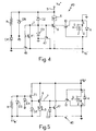
- switches S 1 -S 3 including bipolar transistors and Schottky diodes is shown in Figures 4 and 5 wherein the components are turned around to show more clearly the behaviour of the circuit in two different operating conditions.
- switch S 1 may be represented by transistor T1, switch S 2 by Schottky diode D2, and switch S 3 by Schottky diode D3; and to ensure correct operation of the circuit, this also presents a further two Schottky diodes D4, D5, and a resistor R.
- NPN transistor T1 is shown turned upside down in Figures 4 and 5 to take into account the different voltage conditions involved.
- transistor T1 presents the collector terminal connected to isolating region 7 (shown as a line), the emitter terminal connected to drain terminal D of VDMOS 2, and the base terminal connected to node 45;
- Schottky diode D2 presents the anode connected to isolating region 7, and the cathode connected to input terminal 5;
- Schottky diode D3 presents the anode connected to isolating region 7, and the cathode grounded.
- Node 45 is grounded via Schottky diode D4 (with its anode connected to node 45), and is connected to input terminal 5 via a resistor R and Schottky diode D5. Resistor R and diode D5 are connected parallel to each other, with the anode of D5 connected to node 45.
- Figures 4 and 5 also show two parasitic transistors 47 and 48 associated with the Schottky diodes.
- Figure 6 showing a possible implementation of part of circuit 40. More specifically Figure 6 shows a cross section of a wafer of semiconductor material in which the components are implemented using the same technology as in Figure 2, and wherein any parts common to both Figures 6 and 2 are shown using the same numbering system.
- FIG 6 shows the implementation of transistor T1 and one of the Schottky diodes. More specifically, transistor T1 is implemented by a vertical transistor including a P-type buried region 50 (forming the base region) separated from buried region 20 in which the CMOS components are formed and in which the Schottky diodes may be formed. Over buried region 50, there is provided an N-well 51 isolated by an isolating region 52 to be connected electrically to node 45 by base contacts 53 and metal lines (not shown). N-well 51 houses an N + -type region 55 connected to isolating region 22 by contact 56 and a metal line (not shown).
- the Schottky diode implemented over buried region 20 comprises an N-well 60 isolated from the other well regions 24, 25 by a portion of isolating region 22, and housing an N + -type region 61.
- Region 61 is connected to a contact 62 for connection (for example) to input terminal 5 (diodes D2, D5) or ground (diodes D3, D4); while N-well 60 is connected to a contact 63 (with which it forms a Schottky barrier) connected, for example, to isolating region 22 (diodes D3, D5) or to node 45 (diodes D4, D5).
- Regions 51 and 55 constituting the collector of transistor T1 are formed simultaneously with N-well regions 24, 25, 60 and N + -type regions 29, 30, 61.
- the Schottky diode is associated to a parasitic transistor formed by regions 61, 60 (emitter or collector), 22, 20 (base) and 12, 11 (collector or emitter).
- diodes D3 and D4 are associated to transistors 47, 48 having the emitter formed by regions 11, 12 in Figure 6, the base formed by isolating region 22, and the collector formed by region 61.
- diodes D2 and D5 are associated to respective parasitic transistors similar to parasitic transistor T1 and therefore not shown.
- circuit 40 is shown with a positive input voltage V IN and a negative drain voltage V D .
- transistor T1 is turned on (saturated) and, like switch S 1 in Figure 3, maintains isolating region 7 at a potential close to drain voltage V D .
- parasitic transistor 9 "sees" a very low base-emitter voltage drop which is insufficient to turn it on despite the charges injected by parasitic transistor 10.
- diodes D3, D2 and D5 are reverse biased; diode D4 is turned on and biases the base of T1; and, being insufficiently biased like parasitic transistor 9, parasitic transistors 47 and 48 are also turned off.
- Diode D4 and resistor R ensure that, during the falling half wave of voltage V D , transistor T1 is turned on before parasitic transistors 9, 10, thus preventing parasitic transistors 9, 10 from being turned on.
- T1 "sees" a slightly higher base-emitter voltage drop - equal to V D + V F (where V F is the voltage drop over diode D4) - than transistor 10 which sees a base-emitter voltage drop equal to V D . Consequently, as V D falls, and thanks also to resistor R supplying the base of transistor T1, T1 is turned on in advance of transistor 10, thus preventing any problems arising as V D falls.
- Figure 5 shows the Figure 4 circuit modified to illustrate the behaviour of the circuit with a negative input voltage V IN and a positive drain voltage V D .
- parasitic transistor 8 which is the one likely to be turned on in the above bias condition, is shown in place of parasitic transistor 9; and transistors T1 and 47 are turned upside down (exchanging the collector for the emitter) to show the possible turn-on condition.
- T1 also represents the parasitic transistor associated with diodes D2 and D5 (as in Figure 4) and the parasitic transistor associated with D3 (as in Figure 4) and D4 (the parasitic transistor of D4 in fact presents a grounded emitter, a base formed by isolating region 7, and a collector formed by layers 11, 12, in exactly the same way as transistor 47).
- parasitic transistor 8 is prevented from being turned on by Schottky diode D2 maintaining isolating region 7 at a voltage close to input voltage V IN (roughly 0.2 V higher) and so producing an insufficient voltage drop at the base-emitter junction of transistor 8 (which requires 0.6-0.7 V for it to be turned on).
- D3, D5 and the relative parasitic transistors are turned off.
- D3 in fact is reverse biased, as is the base-emitter junction of the associated parasitic transistor 47.
- diode D4 whereas D5 is turned on and maintains the base of T1 at the same potential as the emitter, so that T1 remains off (as required, particularly in the case of a high drain voltage V D , for preventing failure of transistor T1).
- parasitic transistor 10 is also turned off, by virtue of its base presenting a higher potential as compared with the emitter and collector.
- diode D3 provides for grounding isolating region 7 when input voltage V IN and drain voltage V D are both positive, or when one is zero and the other is positive. In all these cases, diode D3 is turned on and maintains isolating region 7 at the minimum potential present in the circuit; and transistors 8, 9 and T1 are maintained off.
- Circuit 40 is easily implementable, for example, using the solutions shown in Figure 6.
- the resistor may be integrated using the polysilicon layer forming the gates of the MOSFET transistors (27 and 15 in Figure 6), or exploiting the diffused drain/source regions of the same MOSFET transistors, or by defining a higher-resistivity P-type diffused layer in a region isolated from the power stage.
- FIG. 7 shows a possible implementation of diodes D2, D3 and transistor T1 using the same technique as in Figure 6. Any elements common to both are therefore indicated using the same numbering system with no further description.
- Number 70 in Figure 7 indicates the P-type buried layer over which the diodes are formed, and over which are provided two N-well regions 71, 72 separated by isolating regions 73 similar to regions 22, 23, 52.
- N-well regions 71, 72 house N + -type regions 74, 75 for connection to contacts 76, 77, and are directly contacted by aluminium contacts 78, 79 for forming the Schottky diodes of which regions 71, 72 form the cathodes.
- Contacts 78, 79 (diode anodes) are connected by a metal line 80 for electrically contacting the anodes of Schottky diodes D2 and D3.
- the Figure 7 implementation is characterized by a P + -type ring 81 in N-well region 71, surrounding contact 78 and which provides for increasing the breakdown voltage of diode D2.
- the breakdown voltage of the Schottky diodes is below the maximum input voltage V IN value, the potential of isolating region 7 (anode of diode D2) is unable to follow V IN , thus impairing operation of the device as a whole.
- the above breakdown voltage is limited by the rapid increase in the electric field along the periphery of the metal-semiconductor interface; which problem, however, can be solved by forming a guard ring, such as ring 81, connected to the anode of the diode and located along the edge of the Schottky junction.
- the circuit is easily integrated, and presents a high degree of reliability.
Landscapes
- Metal-Oxide And Bipolar Metal-Oxide Semiconductor Integrated Circuits (AREA)
- Semiconductor Integrated Circuits (AREA)
- Electronic Switches (AREA)
Claims (17)
- Schaltung (40) zur Verhinderung des Durchschaltens von parasitären Bauelementen (8, 9, 10) in einer integrierten Schaltung (1), bestehend aus mindestens einer Leistungsstufe (2), einem Niederspannungs-Bauelement, welches von der Leistungsstufe durch einen trennenden Bereich (7, 22) separiert ist, und einem Referenzpotentialbereich (S, 15), welcher auf ein Referenzpotential (Erde) vorgespannt werden kann; wobei die Leistungsstufe einen Substratbereich (D, 11, 12) vom N-Typ, welcher auf eine Klemmenspannung (VD) mit Bezug auf das Referenzpotential vorgespannt werden kann, umfaßt, der trennende Bereich (7, 22) Leitfähigkeit vom P-Typ aufweist und das Niederspannungs-Bauelement einen Eingangsbereich (6) vom N-Typ umfaßt, welcher auf eine Eingangsspannung (VIN) vorgespannt werden kann; dadurch gekennzeichnet daß sie schaltbare leitfähige Bahnen (L1 - L3) umfaßt, die elektrisch zwischen dem trennenden Bereich (7) auf der einen Seite und dem Substratbereich (D, 11, 12), dem Eingangsbereich (6) und dem Referenzpotentialbereich (S, 15) auf der anderen Seite zum elektrischen Verbinden zu jedem Zeitpunkt des trennenden Bereiches mit demjenigen Bereich aus dem Substrat-, Eingangs- und Referenzpotentialbereich, welcher das niedrigste Potential aufweist, geschaltet sind.
- Schaltung nach Anspruch 1, dadurch gekennzeichnet, daß jede der schaltbaren leitfähigen Bahnen (L1 - L3) einen gesteuerten Schalter (S1 - S3) umfaßt.
- Schaltung nach Anspruch 2, dadurch gekennzeichnet, daß die gesteuerten Schalter (S1 - S3) spannungsgesteuert sind.
- Schaltung nach Anspruch 3, dadurch gekennzeichnet, daß sie einen ersten Schalter (S1) umfaßt, welcher einen ersten Anschluß, der mit dem trennenden Bereich (7) verbunden ist, und einen zweiten Anschluß, der mit dem Substratbereich (D) verbunden ist, zum elektrischen Verbinden des trennenden Bereiches mit diesem Substratbereich, wenn die Eingangsspannung (VIN) größer oder gleich dem Referenzpotential ist und die Klemmenspannung (VD) geringer als das Referenzpotential ist, aufweist.
- Schaltung nach Anspruch 4, dadurch gekennzeichnet, daß der erste Schalter (S1) ein Transistor (T1) ist, der einen Steueranschluß, welcher mit dem Referenzpotentialbereich (S) verbunden ist, aufweist.
- Schaltung nach Anspruch 5, dadurch gekennzeichnet, daß der Transistor (T1) ein bipolarer Transistor ist.
- Schaltung nach Anspruch 6, dadurch gekennzeichnet, daß der Transistor ein Vertikaltransistor ist, der den zweiten Anschluß, der von dem Substratbereich (11, 12) gebildet wird, aufweist.
- Schaltung nach einem der vorangegangenen Ansprüche 5 bis 7, dadurch gekennzeichnet, daß sie eine Niederspannungsabfall-Diode (D4), die elektrisch zwischen dem Steueranschluß des Transistors (T1) und dem Referenzpotentialbereich (S) geschaltet ist, umfaßt.
- Schaltung nach Anspruch 8, dadurch gekennzeichnet, daß sie einen Vorspannungswiderstand (R) umfaßt, der elektrisch zwischen den Eingangsbereich (6) und den Steueranschluß des Transistors (T1) geschaltet ist.
- Schaltung nach einem der Ansprüche 5 bis 9, dadurch gekennzeichnet, daß sie eine Niederspannungsabfall-Diode (D5) umfaßt, die elektrisch zwischen den Steueranschluß des Transistors (T1) und den Eingangsbereich (6) geschaltet ist, zum Halten des Transistors im sperrenden Zustand, wenn die Eingangsspannung (VIN) niedriger und die Klemmenspannung höher als das Referenzpotential ist.
- Schaltung nach einem der Ansprüche 3 bis 10, dadurch gekennzeichnet, daß sie einen zweiten Schalter (S2) umfaßt, der elektrisch zwischen den trennenden Bereich (7) und den Eingangsbereich (6) geschaltet ist, zum elektrischen Verbinden des trennenden Bereiches mit dem Eingangsbereich, wenn die Eingangsspannung (VIN) niedriger und die Klemmenspannung (VD) höher als das Referenzpotential ist.
- Schaltung nach Anspruch 11, dadurch gekennzeichnet, daß der zweite Schalter (S2) eine Niederspannungsabfall-Diode (D2) ist.
- Schaltung nach einem der Ansprüche 3 bis 12, dadurch gekennzeichnet, daß sie einen dritten Schalter (S3) umfaßt, der elektrisch zwischen den trennenden Bereich (7) und den Referenzpotentialbereich (S) geschaltet ist, zum elektrischen Verbinden des trennenden Bereiches mit dem Referenzpotentialbereich, wenn die Eingangsspannung (VIN) höher als oder gleich wie, und die Klemmenspannung (VD) höher als das Referenzpotential ist.
- Schaltung nach Anspruch 13, dadurch gekennzeichnet, daß der dritte Schalter (S3) eine Niederspannungsabfall-Diode (D3) ist.
- Schaltung nach einem der Ansprüche 8 bis 14, dadurch gekennzeichnet, daß die Niedrigspannungsabfall-Dioden (D2 - D5) Schottky-Dioden sind.
- Schaltung nach Anspruch 15, worin jede der Schottky-Dioden (D2 - D5) durch eine Schottky-Übergangszone zwischen einem Halbleiterbereich (71) und einer Metallelektrode (78) gebildet ist, welche einen Anoden- bzw. einen Kathodenbereich bilden, und jede der Schottky-Dioden einen Schutzring (81) vom P-Typ aufweist, der elektrisch mit ihrem Anodenbereich verbunden ist und ihren Halbleiterbereich (71) entlang dem Rand der Schottky-Übergangszone umgibt.
- Schaltung nach einem der vorangegangenen Ansprüche, worin die Leistungsstufe einen MOSFET-Leistungstransistor (2), der einen Drain-(D)- und einen Source-(S)-Bereich aufweist, umfaßt, wobei der Substratbereich (11, 12) den Drainbereich (D) des MOSFET-Leistungstransistors bildet und der Referenzpotentialbereich mit dem Sourcebereich (S) des MOSFET-Leistungstransistors verbunden ist.
Priority Applications (4)
| Application Number | Priority Date | Filing Date | Title |
|---|---|---|---|
| EP94830444A EP0703620B1 (de) | 1994-09-21 | 1994-09-21 | Schaltung zur Verhinderung der Zündung von parasitären Bauelementen in integrierten Schaltungen bestehend aus einer Leistungsstufe und einer Niederspannungssteuerschaltung |
| DE69426565T DE69426565T2 (de) | 1994-09-21 | 1994-09-21 | Schaltung zur Verhinderung des Durchschaltens von parasitären Bauelementen in integrierten Schaltungen bestehend aus einer Leistungsstufe un einer Niederspannungssteuerschaltung |
| US08/529,805 US5661430A (en) | 1994-09-21 | 1995-09-19 | Circuit for preventing operation of parasitic components in integrated circuits having a power stage and low-voltage control circuitry |
| JP7243236A JP2810641B2 (ja) | 1994-09-21 | 1995-09-21 | 集積回路の寄生要素の導通を防止する回路 |
Applications Claiming Priority (1)
| Application Number | Priority Date | Filing Date | Title |
|---|---|---|---|
| EP94830444A EP0703620B1 (de) | 1994-09-21 | 1994-09-21 | Schaltung zur Verhinderung der Zündung von parasitären Bauelementen in integrierten Schaltungen bestehend aus einer Leistungsstufe und einer Niederspannungssteuerschaltung |
Publications (2)
| Publication Number | Publication Date |
|---|---|
| EP0703620A1 EP0703620A1 (de) | 1996-03-27 |
| EP0703620B1 true EP0703620B1 (de) | 2001-01-10 |
Family
ID=8218527
Family Applications (1)
| Application Number | Title | Priority Date | Filing Date |
|---|---|---|---|
| EP94830444A Expired - Lifetime EP0703620B1 (de) | 1994-09-21 | 1994-09-21 | Schaltung zur Verhinderung der Zündung von parasitären Bauelementen in integrierten Schaltungen bestehend aus einer Leistungsstufe und einer Niederspannungssteuerschaltung |
Country Status (4)
| Country | Link |
|---|---|
| US (1) | US5661430A (de) |
| EP (1) | EP0703620B1 (de) |
| JP (1) | JP2810641B2 (de) |
| DE (1) | DE69426565T2 (de) |
Families Citing this family (10)
| Publication number | Priority date | Publication date | Assignee | Title |
|---|---|---|---|---|
| JP3036423B2 (ja) * | 1996-02-06 | 2000-04-24 | 日本電気株式会社 | 半導体装置 |
| DE69624493T2 (de) | 1996-12-09 | 2003-06-26 | Stmicroelectronics S.R.L., Agrate Brianza | Vorrichtung und Verfahren zur Unterdrückung von parasitären Effekten in einer integrierten Schaltung mit pn-Isolationszonen |
| WO1998033274A1 (fr) * | 1997-01-24 | 1998-07-30 | Hitachi, Ltd. | Circuit interrupteur d'alimentation |
| US6225673B1 (en) * | 1998-03-03 | 2001-05-01 | Texas Instruments Incorporated | Integrated circuit which minimizes parasitic action in a switching transistor pair |
| DE69902877D1 (de) | 1999-04-30 | 2002-10-17 | St Microelectronics Srl | Integrierter Schaltkreis mit einer Leistungsschaltung und einer Steuerschaltung, ohne parasitäre Ströme |
| DE19928762C1 (de) * | 1999-06-23 | 2000-11-23 | Siemens Ag | Schaltungsanordnung zur Verhinderung der Injektion von Minoritätsladungsträgern in das Substrat |
| EP1221718A1 (de) * | 2001-01-08 | 2002-07-10 | STMicroelectronics S.r.l. | Integriertes Leistungsbauelement mit verbesserter Effizienz und reduzierten Gesamtabmessungen |
| EP1965425A1 (de) * | 2007-03-01 | 2008-09-03 | Infineon Technologies Austria AG | Integrierte Schaltungsanordnung mit Gegenspannungsschutz |
| US8013475B2 (en) | 2007-03-15 | 2011-09-06 | Infineon Technologies Ag | Reverse voltage protected integrated circuit arrangement for multiple supply lines |
| CN104347627A (zh) * | 2014-09-18 | 2015-02-11 | 成都星芯微电子科技有限公司 | 基于场效应管充电的半导体启动器件及制造工艺 |
Family Cites Families (6)
| Publication number | Priority date | Publication date | Assignee | Title |
|---|---|---|---|---|
| US3990092A (en) * | 1974-01-11 | 1976-11-02 | Hitachi, Ltd. | Resistance element for semiconductor integrated circuit |
| JPS5742145A (en) * | 1980-08-26 | 1982-03-09 | Mitsubishi Electric Corp | Semiconductor integrated circuit device |
| FR2636481B1 (fr) * | 1988-09-14 | 1990-11-30 | Sgs Thomson Microelectronics | Diode active integrable |
| US5051612A (en) * | 1989-02-10 | 1991-09-24 | Texas Instruments Incorporated | Prevention of parasitic mechanisms in junction isolated devices |
| IT1231541B (it) * | 1989-07-25 | 1991-12-17 | Sgs Thomson Microelectronics | Dispositivo di protezione contro gli effetti parassiti provocati da impulsi negativi di tensione di alimentazione in circuiti integrati monolitici includenti un dispositivo di potenza per il pilotaggio di un carico induttivo ed un dispositivo di controllo per detto dispositivo di potenza. |
| IT1252623B (it) * | 1991-12-05 | 1995-06-19 | Sgs Thomson Microelectronics | Dispositivo a semiconduttore comprendente almeno un transistor di potenza e almeno un circuito di comando, con circuito di isolamento dinamico,integrati in maniera monolitica nella stessa piastrina |
-
1994
- 1994-09-21 DE DE69426565T patent/DE69426565T2/de not_active Expired - Fee Related
- 1994-09-21 EP EP94830444A patent/EP0703620B1/de not_active Expired - Lifetime
-
1995
- 1995-09-19 US US08/529,805 patent/US5661430A/en not_active Expired - Lifetime
- 1995-09-21 JP JP7243236A patent/JP2810641B2/ja not_active Expired - Fee Related
Also Published As
| Publication number | Publication date |
|---|---|
| EP0703620A1 (de) | 1996-03-27 |
| US5661430A (en) | 1997-08-26 |
| JPH08227991A (ja) | 1996-09-03 |
| JP2810641B2 (ja) | 1998-10-15 |
| DE69426565T2 (de) | 2001-05-31 |
| DE69426565D1 (de) | 2001-02-15 |
Similar Documents
| Publication | Publication Date | Title |
|---|---|---|
| US6288424B1 (en) | Semiconductor device having LDMOS transistors and a screening layer | |
| KR100305238B1 (ko) | Esd보호를위한실리콘제어정류기 | |
| US4825275A (en) | Integrated bipolar-CMOS circuit isolation for providing different backgate and substrate bias | |
| KR930010827B1 (ko) | 반도체장치 | |
| US6049119A (en) | Protection circuit for a semiconductor device | |
| US5963407A (en) | Overvoltage protection device for the protection of a power transistor having a MOS control terminal | |
| US5559348A (en) | Semiconductor device having insulated gate bipolar transistor | |
| US8686531B2 (en) | Structure and method for forming a guard ring to protect a control device in a power semiconductor IC | |
| JPH0685441B2 (ja) | 半導体装置 | |
| US5087579A (en) | Method for fabricating an integrated bipolar-CMOS circuit isolation for providing different backgate and substrate bias | |
| US5604655A (en) | Semiconductor protection circuit and semiconductor protection device | |
| US4912054A (en) | Integrated bipolar-CMOS circuit isolation process for providing different backgate and substrate bias | |
| US20080023767A1 (en) | High voltage electrostatic discharge protection devices and electrostatic discharge protection circuits | |
| EP0703620B1 (de) | Schaltung zur Verhinderung der Zündung von parasitären Bauelementen in integrierten Schaltungen bestehend aus einer Leistungsstufe und einer Niederspannungssteuerschaltung | |
| US6878996B2 (en) | MOS power transistor | |
| JPH09129762A (ja) | 半導体装置 | |
| US6323522B1 (en) | Silicon on insulator thick oxide structure and process of manufacture | |
| US20080135941A1 (en) | Modulated trigger device | |
| US5414292A (en) | Junction-isolated floating diode | |
| EP0424926A2 (de) | Integrierter Bi-CMOS-Schaltkreis | |
| JP4531276B2 (ja) | 半導体装置 | |
| JP3663258B2 (ja) | 制御回路内蔵絶縁ゲート型半導体装置 | |
| US6927460B1 (en) | Method and structure for BiCMOS isolated NMOS transistor | |
| KR20070053980A (ko) | 트랜지스터에 프리휠링 다이오드가 구현된 고집적회로 | |
| KR100867572B1 (ko) | 고전압 섬 영역 내에 바이폴라 트랜지스터가 내장된고전압 집적 회로 |
Legal Events
| Date | Code | Title | Description |
|---|---|---|---|
| PUAI | Public reference made under article 153(3) epc to a published international application that has entered the european phase |
Free format text: ORIGINAL CODE: 0009012 |
|
| 17P | Request for examination filed |
Effective date: 19950512 |
|
| AK | Designated contracting states |
Kind code of ref document: A1 Designated state(s): DE FR GB IT |
|
| 17Q | First examination report despatched |
Effective date: 19970923 |
|
| RAP3 | Party data changed (applicant data changed or rights of an application transferred) |
Owner name: CONSORZIO PER LA RICERCA SULLA MICROELETTRONICA N Owner name: STMICROELECTRONICS S.R.L. |
|
| GRAG | Despatch of communication of intention to grant |
Free format text: ORIGINAL CODE: EPIDOS AGRA |
|
| 17Q | First examination report despatched |
Effective date: 19970923 |
|
| GRAG | Despatch of communication of intention to grant |
Free format text: ORIGINAL CODE: EPIDOS AGRA |
|
| GRAH | Despatch of communication of intention to grant a patent |
Free format text: ORIGINAL CODE: EPIDOS IGRA |
|
| GRAH | Despatch of communication of intention to grant a patent |
Free format text: ORIGINAL CODE: EPIDOS IGRA |
|
| GRAA | (expected) grant |
Free format text: ORIGINAL CODE: 0009210 |
|
| AK | Designated contracting states |
Kind code of ref document: B1 Designated state(s): DE FR GB IT |
|
| REF | Corresponds to: |
Ref document number: 69426565 Country of ref document: DE Date of ref document: 20010215 |
|
| ET | Fr: translation filed | ||
| ITF | It: translation for a ep patent filed | ||
| PLBE | No opposition filed within time limit |
Free format text: ORIGINAL CODE: 0009261 |
|
| STAA | Information on the status of an ep patent application or granted ep patent |
Free format text: STATUS: NO OPPOSITION FILED WITHIN TIME LIMIT |
|
| REG | Reference to a national code |
Ref country code: GB Ref legal event code: IF02 |
|
| 26N | No opposition filed | ||
| PGFP | Annual fee paid to national office [announced via postgrant information from national office to epo] |
Ref country code: DE Payment date: 20031002 Year of fee payment: 10 |
|
| PGFP | Annual fee paid to national office [announced via postgrant information from national office to epo] |
Ref country code: FR Payment date: 20040908 Year of fee payment: 11 |
|
| PGFP | Annual fee paid to national office [announced via postgrant information from national office to epo] |
Ref country code: GB Payment date: 20040915 Year of fee payment: 11 |
|
| PG25 | Lapsed in a contracting state [announced via postgrant information from national office to epo] |
Ref country code: DE Free format text: LAPSE BECAUSE OF NON-PAYMENT OF DUE FEES Effective date: 20050401 |
|
| PG25 | Lapsed in a contracting state [announced via postgrant information from national office to epo] |
Ref country code: IT Free format text: LAPSE BECAUSE OF NON-PAYMENT OF DUE FEES;WARNING: LAPSES OF ITALIAN PATENTS WITH EFFECTIVE DATE BEFORE 2007 MAY HAVE OCCURRED AT ANY TIME BEFORE 2007. THE CORRECT EFFECTIVE DATE MAY BE DIFFERENT FROM THE ONE RECORDED. Effective date: 20050921 Ref country code: GB Free format text: LAPSE BECAUSE OF NON-PAYMENT OF DUE FEES Effective date: 20050921 |
|
| GBPC | Gb: european patent ceased through non-payment of renewal fee |
Effective date: 20050921 |
|
| PG25 | Lapsed in a contracting state [announced via postgrant information from national office to epo] |
Ref country code: FR Free format text: LAPSE BECAUSE OF NON-PAYMENT OF DUE FEES Effective date: 20060531 |
|
| REG | Reference to a national code |
Ref country code: FR Ref legal event code: ST Effective date: 20060531 |