EP0703623A1 - Procédé de fabrication d'une structure de circuit intégré verticale - Google Patents
Procédé de fabrication d'une structure de circuit intégré verticale Download PDFInfo
- Publication number
- EP0703623A1 EP0703623A1 EP95113414A EP95113414A EP0703623A1 EP 0703623 A1 EP0703623 A1 EP 0703623A1 EP 95113414 A EP95113414 A EP 95113414A EP 95113414 A EP95113414 A EP 95113414A EP 0703623 A1 EP0703623 A1 EP 0703623A1
- Authority
- EP
- European Patent Office
- Prior art keywords
- substrate
- main surface
- via holes
- layers
- etching
- Prior art date
- Legal status (The legal status is an assumption and is not a legal conclusion. Google has not performed a legal analysis and makes no representation as to the accuracy of the status listed.)
- Granted
Links
Images

Classifications
-
- H—ELECTRICITY
- H10—SEMICONDUCTOR DEVICES; ELECTRIC SOLID-STATE DEVICES NOT OTHERWISE PROVIDED FOR
- H10D—INORGANIC ELECTRIC SEMICONDUCTOR DEVICES
- H10D88/00—Three-dimensional [3D] integrated devices
-
- H—ELECTRICITY
- H10—SEMICONDUCTOR DEVICES; ELECTRIC SOLID-STATE DEVICES NOT OTHERWISE PROVIDED FOR
- H10D—INORGANIC ELECTRIC SEMICONDUCTOR DEVICES
- H10D84/00—Integrated devices formed in or on semiconductor substrates that comprise only semiconducting layers, e.g. on Si wafers or on GaAs-on-Si wafers
- H10D84/01—Manufacture or treatment
- H10D84/02—Manufacture or treatment characterised by using material-based technologies
- H10D84/03—Manufacture or treatment characterised by using material-based technologies using Group IV technology, e.g. silicon technology or silicon-carbide [SiC] technology
- H10D84/038—Manufacture or treatment characterised by using material-based technologies using Group IV technology, e.g. silicon technology or silicon-carbide [SiC] technology using silicon technology, e.g. SiGe
-
- H—ELECTRICITY
- H10—SEMICONDUCTOR DEVICES; ELECTRIC SOLID-STATE DEVICES NOT OTHERWISE PROVIDED FOR
- H10D—INORGANIC ELECTRIC SEMICONDUCTOR DEVICES
- H10D88/00—Three-dimensional [3D] integrated devices
- H10D88/01—Manufacture or treatment
-
- H—ELECTRICITY
- H10—SEMICONDUCTOR DEVICES; ELECTRIC SOLID-STATE DEVICES NOT OTHERWISE PROVIDED FOR
- H10W—GENERIC PACKAGES, INTERCONNECTIONS, CONNECTORS OR OTHER CONSTRUCTIONAL DETAILS OF DEVICES COVERED BY CLASS H10
- H10W20/00—Interconnections in chips, wafers or substrates
- H10W20/01—Manufacture or treatment
- H10W20/021—Manufacture or treatment of interconnections within wafers or substrates
- H10W20/023—Manufacture or treatment of interconnections within wafers or substrates the interconnections being through-semiconductor vias
-
- H—ELECTRICITY
- H10—SEMICONDUCTOR DEVICES; ELECTRIC SOLID-STATE DEVICES NOT OTHERWISE PROVIDED FOR
- H10W—GENERIC PACKAGES, INTERCONNECTIONS, CONNECTORS OR OTHER CONSTRUCTIONAL DETAILS OF DEVICES COVERED BY CLASS H10
- H10W20/00—Interconnections in chips, wafers or substrates
- H10W20/01—Manufacture or treatment
- H10W20/021—Manufacture or treatment of interconnections within wafers or substrates
- H10W20/023—Manufacture or treatment of interconnections within wafers or substrates the interconnections being through-semiconductor vias
- H10W20/0234—Manufacture or treatment of interconnections within wafers or substrates the interconnections being through-semiconductor vias comprising etching via holes that stop on pads or on electrodes
-
- H—ELECTRICITY
- H10—SEMICONDUCTOR DEVICES; ELECTRIC SOLID-STATE DEVICES NOT OTHERWISE PROVIDED FOR
- H10W—GENERIC PACKAGES, INTERCONNECTIONS, CONNECTORS OR OTHER CONSTRUCTIONAL DETAILS OF DEVICES COVERED BY CLASS H10
- H10W20/00—Interconnections in chips, wafers or substrates
- H10W20/01—Manufacture or treatment
- H10W20/021—Manufacture or treatment of interconnections within wafers or substrates
- H10W20/023—Manufacture or treatment of interconnections within wafers or substrates the interconnections being through-semiconductor vias
- H10W20/0245—Manufacture or treatment of interconnections within wafers or substrates the interconnections being through-semiconductor vias comprising use of blind vias during the manufacture
-
- H—ELECTRICITY
- H10—SEMICONDUCTOR DEVICES; ELECTRIC SOLID-STATE DEVICES NOT OTHERWISE PROVIDED FOR
- H10W—GENERIC PACKAGES, INTERCONNECTIONS, CONNECTORS OR OTHER CONSTRUCTIONAL DETAILS OF DEVICES COVERED BY CLASS H10
- H10W20/00—Interconnections in chips, wafers or substrates
- H10W20/20—Interconnections within wafers or substrates, e.g. through-silicon vias [TSV]
- H10W20/211—Through-semiconductor vias, e.g. TSVs
- H10W20/218—Through-semiconductor vias, e.g. TSVs in silicon-on-insulator [SOI] wafers
-
- H—ELECTRICITY
- H10—SEMICONDUCTOR DEVICES; ELECTRIC SOLID-STATE DEVICES NOT OTHERWISE PROVIDED FOR
- H10W—GENERIC PACKAGES, INTERCONNECTIONS, CONNECTORS OR OTHER CONSTRUCTIONAL DETAILS OF DEVICES COVERED BY CLASS H10
- H10W90/00—Package configurations
-
- H—ELECTRICITY
- H10—SEMICONDUCTOR DEVICES; ELECTRIC SOLID-STATE DEVICES NOT OTHERWISE PROVIDED FOR
- H10W—GENERIC PACKAGES, INTERCONNECTIONS, CONNECTORS OR OTHER CONSTRUCTIONAL DETAILS OF DEVICES COVERED BY CLASS H10
- H10W90/00—Package configurations
- H10W90/20—Configurations of stacked chips
- H10W90/297—Configurations of stacked chips characterised by the through-semiconductor vias [TSVs] in the stacked chips
-
- Y—GENERAL TAGGING OF NEW TECHNOLOGICAL DEVELOPMENTS; GENERAL TAGGING OF CROSS-SECTIONAL TECHNOLOGIES SPANNING OVER SEVERAL SECTIONS OF THE IPC; TECHNICAL SUBJECTS COVERED BY FORMER USPC CROSS-REFERENCE ART COLLECTIONS [XRACs] AND DIGESTS
- Y10—TECHNICAL SUBJECTS COVERED BY FORMER USPC
- Y10S—TECHNICAL SUBJECTS COVERED BY FORMER USPC CROSS-REFERENCE ART COLLECTIONS [XRACs] AND DIGESTS
- Y10S438/00—Semiconductor device manufacturing: process
- Y10S438/975—Substrate or mask aligning feature
Definitions
- the invention relates to a method for producing a vertical integrated circuit structure.
- Vertical circuit structures play an important role in three-dimensional integration.
- Three-dimensional integration is the vertical connection of components that were manufactured using planar technology.
- the advantages of a three-dimensionally integrated microelectronic system include the higher packing densities and switching speeds that can be achieved with the same design rules compared to two-dimensional systems. The latter is due, on the one hand, to shorter line paths between the individual components or circuits, and, on the other hand, to the possibility of parallel information processing.
- the increase in the performance of the system is optimal when implementing a connection technology with freely selectable, highly integrable vertical contacts.
- Y. Akasaka, Proc. IEEE 74 (1986) 1703 proposes to deposit and recrystallize polycrystalline silicon on a completely processed component layer, so that further components can be produced in the recrystallized layer.
- Disadvantages of this method are the yield-reducing degradation of the components in the lower level due to the high thermal load during the recrystallization process, and the necessary serial processing of the overall system. The latter is conditional on the one hand long throughput times in production and secondly results in a reduction in yield by adding up the process-related failures. Both increase the manufacturing costs considerably compared to processing the individual levels separately from one another in different substrates.
- CMOS complementary metal-oxide-semiconductor
- JP 63-213943 describes a method for producing a vertical integrated circuit structure, in which the individual component levels are likewise produced separately from one another in different substrates.
- the upper substrate is provided with via holes which penetrate all layers with circuit structures.
- the lower substrate is provided with contact holes which extend to the metallization level of this substrate. After the backside thinning of the upper substrate up to the via holes, the two substrates are joined so that the via holes of the upper substrate lie over the contact holes of the lower substrate, so that a conductive connection between the component levels of both substrates can be produced.
- the alignment marks When connecting two completely processed component substrates, an exact adjustment of the two substrates by means of alignment marks is required before joining. If a rear side structuring is to be avoided, the alignment marks have so far been applied in the area of the front side of the substrates and the adjustment is carried out using the infrared transmitted light method (known, for example, from so-called flip chip bonding).
- the layer sequence of the upper substrate present at the time of the joining together excludes an optical transmitted light adjustment of the component levels to one another in the visible spectral range.
- the use of the infrared transmitted light process requires special equipment that is unusual in semiconductor production, ie a bonding device with integrated infrared transmitted light adjustment.
- the substrates to be adjusted must also only have polished surfaces (handling substrate and lower component substrate), since otherwise the infrared light is diffusely scattered at the interfaces and therefore the alignment marks cannot be imaged.
- the adjustment accuracy is even when using polished surfaces due to the longer wavelength of the infrared light compared to visible light by a factor of two less than when adjusting in the visible spectral range, so that the packing density of the vertical connection only about 25% of what can be achieved with visible light Value.
- the complex layer structure of an integrated circuit with a large number of interfaces and the associated reflections further reduce the accuracy of adjustment in the transmitted light method. Furthermore, this method limits the freedom of design and the choice of substrate, since good radiation transmission is required in the areas of the alignment marks.
- the present invention has for its object to provide a CMOS-compatible method for producing a vertical integrated circuit structure with freely selectable vertical contacts, which enables a high integration density and high yield.
- the individual component layers in different substrates are processed independently of one another and subsequently joined together.
- the finished substrate first substrate; hereinafter referred to as the top substrate
- the top substrate with one or more component layers and metallization levels, the component layers of which are to lie in the finished integrated circuit structure above the component layers of a further substrate (second substrate; hereinafter referred to as the bottom substrate)
- a mask is applied on the front for later etching (eg dry etching) of dielectric layers (eg oxide and / or nitride layers).
- the mask can, for example, be a layer of TiN or can also be produced using an Si sputtering process.
- the top substrate is then provided with vial holes at the front (for example by etching), at which a vertical contact with the underlying component layers of the bottom substrate is later to be produced.
- the via holes should penetrate all component layers and metallization levels present in the top substrate.
- the via holes preferably end a few micrometers below the component layers of the top substrate (claim 5), when using an SOI substrate preferably on the buried oxide layer (claim 6).
- an auxiliary substrate (handling substrate) is applied to the front of the top substrate, for example via an adhesive layer (claim 9).
- the top substrate is then thinned from the back. The thinning can for example by wet chemical etching or by mechanical or chemomechanical grinding (claim 7).
- the buried oxide can serve as an etch stop (claim 6).
- the thinning can take place up to the via holes (claim 5), so that these are then opened on both sides of the substrate.
- Another finished substrate with one or more component layers and metallization levels, the bottom substrate is then connected to the top substrate.
- the front of the bottom substrate ie the surface of the uppermost component layer of the bottom substrate, is preferably provided with a transparent adhesive layer.
- the adhesive layer can simultaneously take on a passivating and / or planarizing function (claim 10). Then the top substrate and bottom substrate are aligned and the back of the top substrate is connected to the front of the bottom substrate.
- the adjustment can be carried out with the aid of split optics using alignment marks in the visible spectral range (claim 2).
- the alignment marks are produced in the top substrate analogously to the via holes, ie preferably by etching alignment structures from the front through all component layers of the top substrate, the alignment marks of the bottom substrate can be contained in the top metallization level of the bottom substrate.
- the handling substrate is removed.
- the existing via holes are now extended from the front of the top substrate through the remaining layers (e.g. oxide layer of the SOI top substrate, adhesive layer, passivation layer of the bottom substrate) to the metallization layer of a metallization level of the bottom substrate (e.g.
- the mask (hard mask) the top substrate serves as an etching mask. Via these via holes, the electrical contact between the metallization of a metallization level of the top and the metallization of a metallization level of the bottom substrate is finally produced.
- the side walls of the via holes are preferably first isolated and contact holes are opened to the metallization level of the top substrate.
- Metallic material is then deposited on the surface of the top substrate and into the via and contact holes. After the structuring of this connection metallization, the vertical integration of the component layers of top and bottom substrates is established.
- the method according to the invention results in a significant reduction in throughput times in the production of the vertical circuit structure and thus in a reduction in production costs.
- CMOS-compatible technologies are used in the method according to the invention, since in particular a rear-side structuring of the substrates can be dispensed with.
- the production of the via holes on the individual substrate i.e.
- the masking layer (hardmask) to the top substrate at the start of the process and remaining this mask until the via holes open allows the etching of oxide or nitride layers, such as those used for passivation, planarization and multilayer metallization, at any later point in time Manufacturing process (stacking). It is therefore no longer necessary to open contact holes in the bottom wafer before the substrates are joined together.
- the inter-chip vias only have to lie within the metal structures of the bottom wafer, so that the necessary design reserves are smaller and thus one higher integration density can be achieved (analogy to the standard process for multilayer metallization).
- a planarization of the bottom wafer with oxide layers can be carried out before the joining, since the oxide layers can later be opened via the mask of the top substrate.
- the formation of cavities when gluing together is thereby considerably reduced and the reliability of the three-dimensional circuit structure is increased.
- Another advantage of the method is the possible use of SOI substrates as top substrates, since the buried oxide layer can also be easily etched after stacking.
- the advantages of the SOI material e.g. the oxide layer as an etch stop when thinning the top wafer, the great planarity of the back when gluing together, no attack of the via holes by the etching solution or the CMP (Chemical Mechanical Polishing) when thinning
- the advantages of the SOI material e.g. the oxide layer as an etch stop when thinning the top wafer, the great planarity of the back when gluing together, no attack of the via holes by the etching solution or the CMP (Chemical Mechanical Polishing) when thinning
- the vertical contacts can also be realized due to the possibility of etching via the mask of the top substrate up to any metallization levels of the bottom wafer or bottom stack. This enables access to any metallization levels of the stack, so that there is great freedom of design for the integration.
- Another advantage of the method is that split optics in the visible spectral range can be used to adjust the individual component layers one above the other. In contrast to transmitted light methods, therefore, neither the layer sequence above the alignment marks in the top substrate nor the layer sequence below the alignment marks in the bottom substrate need to be transparent. A higher adjustment accuracy and thus a higher packing density can be achieved in comparison to infrared transmission methods.
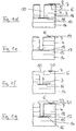
- the top substrate 1 is an SOI wafer (2: silicon; 3: silicon dioxide; 4: silicon) with completely processed MOS circuits in the chip level 5 and three-layer metallization, passivated with an oxide / nitride protective layer 7, as shown in FIG. 1a shown.
- the metallization 6 of the top metallization level is, for example, an aluminum alloy. Undoped and doped oxide layers are located below the metallization level. Titanium nitride 8 and a layer serving as a hard mask, such as plasma oxide 9, are first deposited as masking layers for subsequent dry etching and a photo technique for the via holes 10 is carried out (photo technique "trench").
- the plasma oxide 9 and the titanium nitride 8 as well as underlying oxide layers of the chip level 5 are anisotropically etched using a lacquer mask. After removing the lacquer, the so-called trench etching process is used to etch to the surface of the buried oxide 3 (SiO2 as an etch stop).
- the result is shown in Fig. 1b.
- a silicon wafer 12 is now glued onto the top wafer 1 as an handling substrate by means of an organic adhesive layer 11, and the top substrate 1 is subsequently thinned mechanically and wet-chemically from the rear.
- the bottom surface of the buried oxide 3 (SiO2) serves as an etch stop.
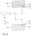
- a polyimide layer 18 is spun onto the bottom plate 13 (14: silicon) with finished MOS circuits in the bottom 15 chip level, three-layer metallization (metallization 16) and passivation 17, so that the surface topography is leveled. Then the top 1 and bottom substrate 13 are bonded in a pane bonding device with split optics (cf. FIG. 1c).
- the split optics 23, which the camera 24 contains, is shown schematically in FIG. 2. After the removal of the handling substrate 12 and the adhesive layer 11, the stack wafer thus created can now be processed further like a standard silicon wafer.
- the buried oxide 3, the adhesive layer 18 and the protective layer 17 over the metal 16 of the bottom metallization are anisotropically etched in the via holes 10.
- the metallization 16 serves as an etching stop (FIG. 1d).
- the titanium nitride layer 8, which served as a mask for the dry etching process, is now removed and ozone-TEOS oxide 19 is deposited. Because of its high conformity during deposition, the latter ensures the electrical isolation of the metallization of the via holes from the silicon substrate given the high aspect ratio of the via holes (FIG. 1e).
- a sidewall passivation is then realized by means of a strongly directed dry etching process (so-called spacer etching process with metallization 16 as an etching stop).
- oxide etching etching stop: metallization 6
- paint and cleaning FIG.
- a titanium nitride layer 21 is first used as an adhesive and barrier layer for the subsequent tungsten metallization 22 ( deposited by W deposition) of the inter-chip vias 10.
- the tungsten / titanium nitride layer 21, 22 is structured (W-etching, TiN-etching / lacquer ashing) with the aid of a last photo technique "Nailhead", so that the vertical connection between top and bottom components is realized (FIG. 1g).
Landscapes
- Internal Circuitry In Semiconductor Integrated Circuit Devices (AREA)
- Electrodes Of Semiconductors (AREA)
- Drying Of Semiconductors (AREA)
Applications Claiming Priority (2)
| Application Number | Priority Date | Filing Date | Title |
|---|---|---|---|
| DE4433846 | 1994-09-22 | ||
| DE4433846A DE4433846C2 (de) | 1994-09-22 | 1994-09-22 | Verfahren zur Herstellung einer vertikalen integrierten Schaltungsstruktur |
Publications (2)
| Publication Number | Publication Date |
|---|---|
| EP0703623A1 true EP0703623A1 (fr) | 1996-03-27 |
| EP0703623B1 EP0703623B1 (fr) | 1999-06-23 |
Family
ID=6528904
Family Applications (1)
| Application Number | Title | Priority Date | Filing Date |
|---|---|---|---|
| EP95113414A Expired - Lifetime EP0703623B1 (fr) | 1994-09-22 | 1995-08-26 | Procédé de fabrication d'une structure de circuit intégré verticale |
Country Status (4)
| Country | Link |
|---|---|
| US (1) | US5766984A (fr) |
| EP (1) | EP0703623B1 (fr) |
| JP (1) | JP3992762B2 (fr) |
| DE (2) | DE4433846C2 (fr) |
Cited By (2)
| Publication number | Priority date | Publication date | Assignee | Title |
|---|---|---|---|---|
| DE10323394A1 (de) * | 2003-05-20 | 2004-12-23 | Fraunhofer-Gesellschaft zur Förderung der angewandten Forschung e.V. | Verfahren und Vorrichtung zum Erzeugen einer elektrischen Kontaktierung zwischen zwei Halbleiterstücken und Anordnung von Halbleiterstücken |
| DE102004056970A1 (de) * | 2004-11-25 | 2006-06-01 | Fraunhofer-Gesellschaft zur Förderung der angewandten Forschung e.V. | Verfahren und Vorrichtung zum Erzeugen einer elektrischen Kontaktierung zwischen zwei Halbleiterstücken durch ein mechanisches Element |
Families Citing this family (40)
| Publication number | Priority date | Publication date | Assignee | Title |
|---|---|---|---|---|
| US6882030B2 (en) | 1996-10-29 | 2005-04-19 | Tru-Si Technologies, Inc. | Integrated circuit structures with a conductor formed in a through hole in a semiconductor substrate and protruding from a surface of the substrate |
| JP3537447B2 (ja) * | 1996-10-29 | 2004-06-14 | トル‐シ・テクノロジーズ・インコーポレイテッド | 集積回路及びその製造方法 |
| ATE254803T1 (de) * | 1997-09-19 | 2003-12-15 | Fraunhofer Ges Forschung | Verdrahtungsverfahren für halbleiter-bauelemente zur verhinderung von produktpiraterie und produktmanipulation, durch das verfahren hergestelltes halbleiter-bauelement und verwendung des halbleiter-bauelements in einer chipkarte |
| DE19813239C1 (de) * | 1998-03-26 | 1999-12-23 | Fraunhofer Ges Forschung | Verdrahtungsverfahren zur Herstellung einer vertikalen integrierten Schaltungsstruktur und vertikale integrierte Schaltungsstruktur |
| DE19818968C2 (de) * | 1998-04-28 | 2000-11-30 | Fraunhofer Ges Forschung | Verfahren zur Herstellung eines Transponders, Verfahren zur Herstellung einer Chipkarte, die einen Transponder aufweist, sowie nach dem erfindungsgemäßen Verfahren hergestellter Transponder und nach dem erfindungsgemäßen Verfahren hergestellte Chipkarte |
| US6168971B1 (en) * | 1998-05-05 | 2001-01-02 | Fujitsu Limited | Method of assembling thin film jumper connectors to a substrate |
| GB9815992D0 (en) * | 1998-07-23 | 1998-09-23 | Secr Defence | Improvements in and relating to microchemical devices |
| DE19856573C1 (de) | 1998-12-08 | 2000-05-18 | Fraunhofer Ges Forschung | Verfahren zur vertikalen Integration von aktiven Schaltungsebenen und unter Verwendung desselben erzeugte vertikale integrierte Schaltung |
| ATE250806T1 (de) | 1999-05-27 | 2003-10-15 | Fraunhofer Ges Forschung | Verfahren zur vertikalen integration von elektrischen bauelementen mittels rückseitenkontaktierung |
| DE19946715C1 (de) * | 1999-09-29 | 2001-05-03 | Infineon Technologies Ag | Verfahren zur dreidimensionalen Integration mikroelektronischer Systeme |
| US6984571B1 (en) * | 1999-10-01 | 2006-01-10 | Ziptronix, Inc. | Three dimensional device integration method and integrated device |
| US6500694B1 (en) * | 2000-03-22 | 2002-12-31 | Ziptronix, Inc. | Three dimensional device integration method and integrated device |
| US6902987B1 (en) | 2000-02-16 | 2005-06-07 | Ziptronix, Inc. | Method for low temperature bonding and bonded structure |
| US6376265B1 (en) * | 2000-04-05 | 2002-04-23 | Advanced Micro Devices, Inc. | Non-contact automatic height sensing using air pressure for die bonding |
| US6563133B1 (en) * | 2000-08-09 | 2003-05-13 | Ziptronix, Inc. | Method of epitaxial-like wafer bonding at low temperature and bonded structure |
| DE60035994T2 (de) * | 2000-10-04 | 2008-06-05 | Qimonda Ag | Verfahren zur Herstellung eines dünnen selbsttragenden Halbleitervorrichtungsfilms und einer dreidimensionalen Halbleitervorrichtung |
| US6410424B1 (en) * | 2001-04-19 | 2002-06-25 | Taiwan Semiconductor Manufacturing Company | Process flow to optimize profile of ultra small size photo resist free contact |
| DE10303643B3 (de) * | 2003-01-30 | 2004-09-09 | X-Fab Semiconductor Foundries Ag | Verfahren zur Herstellung von Substratkontakten bei SOI-Schaltungsstrukturen |
| US7109092B2 (en) | 2003-05-19 | 2006-09-19 | Ziptronix, Inc. | Method of room temperature covalent bonding |
| GB2418063A (en) * | 2004-09-08 | 2006-03-15 | Cambridge Semiconductor Ltd | SOI power device |
| US7829438B2 (en) | 2006-10-10 | 2010-11-09 | Tessera, Inc. | Edge connect wafer level stacking |
| US8513789B2 (en) * | 2006-10-10 | 2013-08-20 | Tessera, Inc. | Edge connect wafer level stacking with leads extending along edges |
| US7901989B2 (en) | 2006-10-10 | 2011-03-08 | Tessera, Inc. | Reconstituted wafer level stacking |
| US7952195B2 (en) * | 2006-12-28 | 2011-05-31 | Tessera, Inc. | Stacked packages with bridging traces |
| CN101809739B (zh) * | 2007-07-27 | 2014-08-20 | 泰塞拉公司 | 具有后应用的衬垫延长部分的重构晶片堆封装 |
| US8193092B2 (en) * | 2007-07-31 | 2012-06-05 | Micron Technology, Inc. | Semiconductor devices including a through-substrate conductive member with an exposed end and methods of manufacturing such semiconductor devices |
| WO2009020572A2 (fr) | 2007-08-03 | 2009-02-12 | Tessera Technologies Hungary Kft. | Ensembles empilés utilisant des tranches reconstituées |
| US8043895B2 (en) * | 2007-08-09 | 2011-10-25 | Tessera, Inc. | Method of fabricating stacked assembly including plurality of stacked microelectronic elements |
| DE102007044685B3 (de) * | 2007-09-19 | 2009-04-02 | Fraunhofer-Gesellschaft zur Förderung der angewandten Forschung e.V. | Elektronisches System und Verfahren zur Herstellung eines dreidimensionalen elektronischen Systems |
| JP5639052B2 (ja) * | 2008-06-16 | 2014-12-10 | テッセラ,インコーポレイテッド | ウェハレベルでの縁部の積重ね |
| DE102008033395B3 (de) * | 2008-07-16 | 2010-02-04 | Austriamicrosystems Ag | Verfahren zur Herstellung eines Halbleiterbauelementes und Halbleiterbauelement |
| US8466542B2 (en) * | 2009-03-13 | 2013-06-18 | Tessera, Inc. | Stacked microelectronic assemblies having vias extending through bond pads |
| DE102010045055B4 (de) | 2010-09-10 | 2019-03-28 | Austriamicrosystems Ag | Verfahren zur Herstellung eines Halbleiterbauelementes mit einer Durchkontaktierung |
| US8466061B2 (en) | 2010-09-23 | 2013-06-18 | Infineon Technologies Ag | Method for forming a through via in a semiconductor element and semiconductor element comprising the same |
| DE102011013228B4 (de) * | 2011-03-07 | 2014-05-28 | Austriamicrosystems Ag | Verfahren zur Herstellung eines Halbleiterbauelements für 3D-Integration |
| US8404557B2 (en) | 2011-04-18 | 2013-03-26 | Infineon Technologies Austria Ag | Method for forming a semiconductor device and a semiconductor device |
| US8614145B2 (en) | 2011-12-14 | 2013-12-24 | Sematech, Inc. | Through substrate via formation processing using sacrificial material |
| DE102013106153B4 (de) * | 2013-03-15 | 2020-06-10 | Taiwan Semiconductor Manufacturing Company, Ltd. | Zwischenverbindungsstruktur für eine gestapelte Vorrichtung und Verfahren |
| DE102014104239A1 (de) | 2014-03-26 | 2015-10-01 | Ev Group E. Thallner Gmbh | Verfahren zur Beschichtung von Kavitäten eines Halbleitersubstrats |
| KR20230097121A (ko) | 2020-10-29 | 2023-06-30 | 아데이아 세미컨덕터 본딩 테크놀로지스 인코포레이티드 | 직접 접합 방법 및 구조체 |
Citations (1)
| Publication number | Priority date | Publication date | Assignee | Title |
|---|---|---|---|---|
| JPS6423564A (en) * | 1987-07-17 | 1989-01-26 | Sharp Kk | Space type semiconductor device |
Family Cites Families (18)
| Publication number | Priority date | Publication date | Assignee | Title |
|---|---|---|---|---|
| US3762038A (en) * | 1970-09-09 | 1973-10-02 | Texas Instruments Inc | Thermal displays using air isolated integrated circuits and methods of making same |
| US4295596A (en) * | 1979-12-19 | 1981-10-20 | Western Electric Company, Inc. | Methods and apparatus for bonding an article to a metallized substrate |
| NL8501773A (nl) * | 1985-06-20 | 1987-01-16 | Philips Nv | Werkwijze voor het vervaardigen van halfgeleiderinrichtingen. |
| US4669175A (en) * | 1985-12-02 | 1987-06-02 | Honeywell Inc. | Front-to-back alignment procedure for Burrus LED's |
| US4829018A (en) * | 1986-06-27 | 1989-05-09 | Wahlstrom Sven E | Multilevel integrated circuits employing fused oxide layers |
| JPH063837B2 (ja) * | 1987-03-03 | 1994-01-12 | シャープ株式会社 | 三次元半導体集積回路の製造方法 |
| US4899921A (en) * | 1988-10-28 | 1990-02-13 | The American Optical Corporation | Aligner bonder |
| CA2044649A1 (fr) * | 1990-06-19 | 1991-12-20 | Masanori Nishiguchi | Methode et appareil de mise sous boitier de dispositifs a semiconducteur |
| US5270261A (en) * | 1991-09-13 | 1993-12-14 | International Business Machines Corporation | Three dimensional multichip package methods of fabrication |
| US5266511A (en) * | 1991-10-02 | 1993-11-30 | Fujitsu Limited | Process for manufacturing three dimensional IC's |
| US5252849A (en) * | 1992-03-02 | 1993-10-12 | Motorola, Inc. | Transistor useful for further vertical integration and method of formation |
| CA2096551A1 (fr) * | 1992-05-22 | 1993-11-23 | Masanori Nishiguchi | Dispositif a semiconducteur |
| US5489554A (en) * | 1992-07-21 | 1996-02-06 | Hughes Aircraft Company | Method of making a 3-dimensional circuit assembly having electrical contacts that extend through the IC layer |
| US5591678A (en) * | 1993-01-19 | 1997-01-07 | He Holdings, Inc. | Process of manufacturing a microelectric device using a removable support substrate and etch-stop |
| US5480820A (en) * | 1993-03-29 | 1996-01-02 | Motorola, Inc. | Method of making a vertically formed neuron transistor having a floating gate and a control gate and a method of formation |
| US5455445A (en) * | 1994-01-21 | 1995-10-03 | Kulite Semiconductor Products, Inc. | Multi-level semiconductor structures having environmentally isolated elements |
| US5380681A (en) * | 1994-03-21 | 1995-01-10 | United Microelectronics Corporation | Three-dimensional multichip package and methods of fabricating |
| DE4433845A1 (de) * | 1994-09-22 | 1996-03-28 | Fraunhofer Ges Forschung | Verfahren zur Herstellung einer dreidimensionalen integrierten Schaltung |
-
1994
- 1994-09-22 DE DE4433846A patent/DE4433846C2/de not_active Expired - Fee Related
-
1995
- 1995-08-26 DE DE59506266T patent/DE59506266D1/de not_active Expired - Lifetime
- 1995-08-26 EP EP95113414A patent/EP0703623B1/fr not_active Expired - Lifetime
- 1995-09-22 JP JP24473395A patent/JP3992762B2/ja not_active Expired - Lifetime
- 1995-09-22 US US08/532,367 patent/US5766984A/en not_active Expired - Lifetime
Patent Citations (1)
| Publication number | Priority date | Publication date | Assignee | Title |
|---|---|---|---|---|
| JPS6423564A (en) * | 1987-07-17 | 1989-01-26 | Sharp Kk | Space type semiconductor device |
Non-Patent Citations (2)
| Title |
|---|
| HAYASHI Y ET AL: "FABRICATION OF THREE-DIMENSIONAL IC USING "CUMULATIVELY BONDED IC" (CUBIC) TECHNOLOGY", SYMPOSIUM ON VLSI TECHNOLOGY, HONOLULU, JUNE 4 - 7, 1990, no. SYMP. 10, 4 June 1990 (1990-06-04), INSTITUTE OF ELECTRICAL AND ELECTRONICS ENGINEERS, pages 95 - 96, XP000164428 * |
| PATENT ABSTRACTS OF JAPAN vol. 013, no. 201 (E - 757) 12 May 1989 (1989-05-12) * |
Cited By (4)
| Publication number | Priority date | Publication date | Assignee | Title |
|---|---|---|---|---|
| DE10323394A1 (de) * | 2003-05-20 | 2004-12-23 | Fraunhofer-Gesellschaft zur Förderung der angewandten Forschung e.V. | Verfahren und Vorrichtung zum Erzeugen einer elektrischen Kontaktierung zwischen zwei Halbleiterstücken und Anordnung von Halbleiterstücken |
| DE10323394B4 (de) * | 2003-05-20 | 2006-09-28 | Fraunhofer-Gesellschaft zur Förderung der angewandten Forschung e.V. | Verfahren zum Erzeugen einer elektrischen Kontaktierung zwischen zwei Halbleiterstücken und Verfahren zum Herstellen einer Anordnung von Halbleiterstücken |
| DE102004056970A1 (de) * | 2004-11-25 | 2006-06-01 | Fraunhofer-Gesellschaft zur Förderung der angewandten Forschung e.V. | Verfahren und Vorrichtung zum Erzeugen einer elektrischen Kontaktierung zwischen zwei Halbleiterstücken durch ein mechanisches Element |
| DE102004056970B4 (de) * | 2004-11-25 | 2008-07-03 | Fraunhofer-Gesellschaft zur Förderung der angewandten Forschung e.V. | Verfahren und Vorrichtung zum Erzeugen einer elektrischen Kontaktierung zwischen zwei Halbleiterstücken durch ein mechanisches Element |
Also Published As
| Publication number | Publication date |
|---|---|
| JPH08213549A (ja) | 1996-08-20 |
| DE59506266D1 (de) | 1999-07-29 |
| DE4433846C2 (de) | 1999-06-02 |
| EP0703623B1 (fr) | 1999-06-23 |
| US5766984A (en) | 1998-06-16 |
| JP3992762B2 (ja) | 2007-10-17 |
| DE4433846A1 (de) | 1996-03-28 |
Similar Documents
| Publication | Publication Date | Title |
|---|---|---|
| EP0703623B1 (fr) | Procédé de fabrication d'une structure de circuit intégré verticale | |
| DE19516487C1 (de) | Verfahren zur vertikalen Integration mikroelektronischer Systeme | |
| DE19813239C1 (de) | Verdrahtungsverfahren zur Herstellung einer vertikalen integrierten Schaltungsstruktur und vertikale integrierte Schaltungsstruktur | |
| EP0862788B1 (fr) | Procede de production d'un composant a semi-conducteur integre verticalement | |
| DE112010000142B4 (de) | Kostenoptimiertes Verfahren zum Bilden von hoch dichten passiven Kondensatoren zum Ersetzen diskreter Kondensatoren unter Verwendung eines kostenoptimierten modularen 3D-Wafer-Wafer-Integrationsschemas | |
| EP0703618B1 (fr) | Procédé pour fabriquer un circuit intégré tridimensionnel | |
| EP0739540B1 (fr) | Procede de fabrication d'un circuit tridimensionnel | |
| EP0703619B1 (fr) | Procédé pour fabriquer un circuit intégré tridimensionnel pour atteindre des systèmes à rendement plus haut | |
| DE4490400C2 (de) | Verfahren zum Bilden von tiefen, leitenden Durchkontaktierungen und eine Verbindungsschicht, die nach diesem Verfahren gebildete Durchkontaktierungen enthält | |
| DE69712968T2 (de) | Metal-Isolator-Metall-Kondensator | |
| DE102014118969B4 (de) | Verfahren zum Herstellen einer 3DIC Dichtungsring-Struktur | |
| DE102020111391A1 (de) | Rückseitenkondensatortechniken | |
| EP1454344B1 (fr) | Proédé de fabrication d'un élément intégré à semiconducteurs comportant un condensateur métal-isolant-métal | |
| DE19834917A1 (de) | Verfahren zum Bilden von selbstausrichtenden Durchgängen in integrierten Schaltungen mit mehreren Metallebenen | |
| DE69330870T2 (de) | Planarisierungsverfahren von einer Halbleitervorrichtung | |
| DE102022100017A1 (de) | Bump-integration mit umverteilungsschicht | |
| DE102020124580A1 (de) | Wafer bonding method | |
| DE102019130124A1 (de) | Funktionale komponente innerhalb einer verbindungsstruktur einer halbleitervorrichtung und verfahren zum bilden derselben | |
| DE102004001853B3 (de) | Verfahren zum Herstellen von Kontaktierungsanschlüssen | |
| DE4221432C2 (de) | Globales Planarisierungsverfahren für integrierte Halbleiterschaltungen oder mikromechanische Bauteile | |
| DE10244077B4 (de) | Verfahren zur Herstellung von Halbleiterbauteilen mit Durchkontaktierung | |
| DE10239218A1 (de) | Verfahren zum Herstellen einer Halbleitervorrichtung und deren Aufbau | |
| DE102023105382A1 (de) | Halbleitervorrichtung und herstellungsverfahren | |
| DE112023004797T5 (de) | Metall-isolator-metall (mim)-kondensatoren mit gekrümmter elektrode | |
| DE4324638A1 (de) | Verfahren zum Herstellen elektrischer Kontakte für integrierte Schaltungen sowie mit derartigen Kontakten ausgebildete integrierte Schaltung |
Legal Events
| Date | Code | Title | Description |
|---|---|---|---|
| PUAI | Public reference made under article 153(3) epc to a published international application that has entered the european phase |
Free format text: ORIGINAL CODE: 0009012 |
|
| AK | Designated contracting states |
Kind code of ref document: A1 Designated state(s): DE FR GB IE IT |
|
| 17P | Request for examination filed |
Effective date: 19960216 |
|
| GRAG | Despatch of communication of intention to grant |
Free format text: ORIGINAL CODE: EPIDOS AGRA |
|
| GRAG | Despatch of communication of intention to grant |
Free format text: ORIGINAL CODE: EPIDOS AGRA |
|
| GRAH | Despatch of communication of intention to grant a patent |
Free format text: ORIGINAL CODE: EPIDOS IGRA |
|
| 17Q | First examination report despatched |
Effective date: 19981113 |
|
| GRAH | Despatch of communication of intention to grant a patent |
Free format text: ORIGINAL CODE: EPIDOS IGRA |
|
| GRAA | (expected) grant |
Free format text: ORIGINAL CODE: 0009210 |
|
| AK | Designated contracting states |
Kind code of ref document: B1 Designated state(s): DE FR GB IE IT |
|
| GBT | Gb: translation of ep patent filed (gb section 77(6)(a)/1977) |
Effective date: 19990705 |
|
| REF | Corresponds to: |
Ref document number: 59506266 Country of ref document: DE Date of ref document: 19990729 |
|
| ET | Fr: translation filed | ||
| REG | Reference to a national code |
Ref country code: IE Ref legal event code: FG4D Free format text: GERMAN |
|
| ITF | It: translation for a ep patent filed | ||
| PLBE | No opposition filed within time limit |
Free format text: ORIGINAL CODE: 0009261 |
|
| STAA | Information on the status of an ep patent application or granted ep patent |
Free format text: STATUS: NO OPPOSITION FILED WITHIN TIME LIMIT |
|
| 26N | No opposition filed | ||
| REG | Reference to a national code |
Ref country code: GB Ref legal event code: IF02 |
|
| PGFP | Annual fee paid to national office [announced via postgrant information from national office to epo] |
Ref country code: DE Payment date: 20140821 Year of fee payment: 20 Ref country code: IE Payment date: 20140820 Year of fee payment: 20 |
|
| PGFP | Annual fee paid to national office [announced via postgrant information from national office to epo] |
Ref country code: FR Payment date: 20140819 Year of fee payment: 20 Ref country code: GB Payment date: 20140821 Year of fee payment: 20 |
|
| PGFP | Annual fee paid to national office [announced via postgrant information from national office to epo] |
Ref country code: IT Payment date: 20140827 Year of fee payment: 20 |
|
| REG | Reference to a national code |
Ref country code: DE Ref legal event code: R071 Ref document number: 59506266 Country of ref document: DE |
|
| REG | Reference to a national code |
Ref country code: GB Ref legal event code: PE20 Expiry date: 20150825 |
|
| REG | Reference to a national code |
Ref country code: IE Ref legal event code: MK9A |
|
| PG25 | Lapsed in a contracting state [announced via postgrant information from national office to epo] |
Ref country code: IE Free format text: LAPSE BECAUSE OF EXPIRATION OF PROTECTION Effective date: 20150826 Ref country code: GB Free format text: LAPSE BECAUSE OF EXPIRATION OF PROTECTION Effective date: 20150825 |