EP0704679A1 - Vorrichtung zur Positionsdetektion - Google Patents
Vorrichtung zur Positionsdetektion Download PDFInfo
- Publication number
- EP0704679A1 EP0704679A1 EP95115434A EP95115434A EP0704679A1 EP 0704679 A1 EP0704679 A1 EP 0704679A1 EP 95115434 A EP95115434 A EP 95115434A EP 95115434 A EP95115434 A EP 95115434A EP 0704679 A1 EP0704679 A1 EP 0704679A1
- Authority
- EP
- European Patent Office
- Prior art keywords
- phase signals
- gain
- signals
- output
- position detecting
- Prior art date
- Legal status (The legal status is an assumption and is not a legal conclusion. Google has not performed a legal analysis and makes no representation as to the accuracy of the status listed.)
- Granted
Links
Images



Classifications
-
- G—PHYSICS
- G01—MEASURING; TESTING
- G01D—MEASURING NOT SPECIALLY ADAPTED FOR A SPECIFIC VARIABLE; ARRANGEMENTS FOR MEASURING TWO OR MORE VARIABLES NOT COVERED IN A SINGLE OTHER SUBCLASS; TARIFF METERING APPARATUS; MEASURING OR TESTING NOT OTHERWISE PROVIDED FOR
- G01D5/00—Mechanical means for transferring the output of a sensing member; Means for converting the output of a sensing member to another variable where the form or nature of the sensing member does not constrain the means for converting; Transducers not specially adapted for a specific variable
- G01D5/12—Mechanical means for transferring the output of a sensing member; Means for converting the output of a sensing member to another variable where the form or nature of the sensing member does not constrain the means for converting; Transducers not specially adapted for a specific variable using electric or magnetic means
- G01D5/244—Mechanical means for transferring the output of a sensing member; Means for converting the output of a sensing member to another variable where the form or nature of the sensing member does not constrain the means for converting; Transducers not specially adapted for a specific variable using electric or magnetic means influencing characteristics of pulses or pulse trains; generating pulses or pulse trains
- G01D5/24471—Error correction
- G01D5/24476—Signal processing
-
- G—PHYSICS
- G01—MEASURING; TESTING
- G01D—MEASURING NOT SPECIALLY ADAPTED FOR A SPECIFIC VARIABLE; ARRANGEMENTS FOR MEASURING TWO OR MORE VARIABLES NOT COVERED IN A SINGLE OTHER SUBCLASS; TARIFF METERING APPARATUS; MEASURING OR TESTING NOT OTHERWISE PROVIDED FOR
- G01D5/00—Mechanical means for transferring the output of a sensing member; Means for converting the output of a sensing member to another variable where the form or nature of the sensing member does not constrain the means for converting; Transducers not specially adapted for a specific variable
- G01D5/12—Mechanical means for transferring the output of a sensing member; Means for converting the output of a sensing member to another variable where the form or nature of the sensing member does not constrain the means for converting; Transducers not specially adapted for a specific variable using electric or magnetic means
- G01D5/244—Mechanical means for transferring the output of a sensing member; Means for converting the output of a sensing member to another variable where the form or nature of the sensing member does not constrain the means for converting; Transducers not specially adapted for a specific variable using electric or magnetic means influencing characteristics of pulses or pulse trains; generating pulses or pulse trains
- G01D5/24471—Error correction
- G01D5/2448—Correction of gain, threshold, offset or phase control
-
- H—ELECTRICITY
- H02—GENERATION; CONVERSION OR DISTRIBUTION OF ELECTRIC POWER
- H02J—ELECTRIC POWER NETWORKS; CIRCUIT ARRANGEMENTS OR SYSTEMS FOR SUPPLYING OR DISTRIBUTING ELECTRIC POWER; SYSTEMS FOR STORING ELECTRIC ENERGY
- H02J3/00—Circuit arrangements for AC mains or AC distribution networks
- H02J3/26—Arrangements for eliminating or reducing asymmetry in polyphase networks
-
- Y—GENERAL TAGGING OF NEW TECHNOLOGICAL DEVELOPMENTS; GENERAL TAGGING OF CROSS-SECTIONAL TECHNOLOGIES SPANNING OVER SEVERAL SECTIONS OF THE IPC; TECHNICAL SUBJECTS COVERED BY FORMER USPC CROSS-REFERENCE ART COLLECTIONS [XRACs] AND DIGESTS
- Y02—TECHNOLOGIES OR APPLICATIONS FOR MITIGATION OR ADAPTATION AGAINST CLIMATE CHANGE
- Y02E—REDUCTION OF GREENHOUSE GAS [GHG] EMISSIONS, RELATED TO ENERGY GENERATION, TRANSMISSION OR DISTRIBUTION
- Y02E40/00—Technologies for an efficient electrical power generation, transmission or distribution
- Y02E40/50—Arrangements for eliminating or reducing asymmetry in polyphase networks
Definitions
- the present invention relates to a position detecting apparatus, and more particularly to an apparatus which generates a high-accuracy position-detective signal by the interpolation of a plurality of detecting signals from a plurality of detection elements.
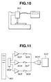
- FIGs. 10 and 11 show a typical position detecting apparatus which detects a position of movable objects.
- This conventional position detecting apparatus is provided with a measuring scale 901 and a MR sensor 902 which is constituted by three units of magnetic resistance elements.
- Three-phase signals outputted from the three magnetic resistance elements of the MR sensor 902 are supplied to sampling circuits 906, 907 and 908 through buffer amplifiers 903, 904 and 905, respectively.
- the sampling circuits 906, 907 and 908 are turned on sequentially so as to supply the analog signals from the buffer amplifiers 903, 904 and 905 to an AD conversion circuit 909 sequentially.
- the AD conversion circuit 909 converts the analog signals to digital signals and supplies them to a central processing unit (CPU) 910.
- the CPU 910 executes a calculating operation for obtaining a position of a movable object as to each of the three-phase signals A, B and C.
- each phase of the three-phase signals A, B and C is shifted from those of the other signals A, B and C by 120°.
- a cycle period of the signal A can be divided into first to sixth intervals. In the first interval, the amplitude of the signals A, B and C are A>C>B. In the second interval, A>B>C. In the third interval, B>A>C.
- the gradient of the line becomes large as shown by a real line in Fig. 8.
- the gradient of the line becomes small as shown by a broken line in Fig. 8. Therefore, in case of a large gradient, the offset of the phase of the signal is detected as if it takes a small value at a point a with respect to the detection signal v in Fig. 8. Further, in case of small gradient, the offset of the phase of the signal is detected as if it take a large value at a point b in Fig. 8. Therefore, it is difficult to execute a accurate position detection according to the offset amount of the phase of the signal in the above-mentioned situation.
- the conventional position detecting apparatus has been arranged so as to detect a maximum value V max and a minimum value V min of the intersections between the phase signals and to obtain a center voltage (V max + V min )/2 , for executing a correction by an offset voltage.
- the convention position detecting apparatus Is arranged to obtain a multiplying factor functioning as a reference amplitude by the calculation of (V max - V min ) and to correct the signals A, B and C by multiplying the obtained multiplying factor with the detection signal, in order to execute a position detection by means of the corrected signal.
- this conventional position detecting apparatus is required to detect the previous maximum value V max and minimum value V min of the intersections since this apparatus executes a position detection by detecting an actual amount of the phase offset according to a ratio ( V-V min )/(V max -V min ) wherein V is a present detected voltage, (V-V min ) is a present deviation, and (V max -V min ) is a maximum deviation.
- Another object of the present invention is to provides a position detecting apparatus which enables the generation of correct position indicative signal without using previously stored data.
- a first aspect of the present invention resides in a position detecting apparatus comprising a sensor which detects a signal recorded on a measuring scale and outputs three-phase signals indicative of the scale recorded signal.
- An offset value calculating means calculates an offset value by calculating the sum of the three-phase signals and by calculating one-third of the sum of the three-phase signals.
- a three-phase signal correcting means corrects the three-phase signals by eliminating an output of the offset value calculating means from each of the three-phase signals.
- a further aspect of the present invention resides in a position detecting apparatus which is further defined by additional elements. That is, the above position detecting apparatus further comprises a sine-wave signal squaring means which generates a signal indicative of a square of one of the three-phase signals.
- a cosine-wave signal squaring means includes a subtracter which calculates a difference between the other two of the three-phase signals, a square calculator which calculates a square of an output of the subtracter, and a calculator which derived one-third of an output of the square calculator.
- a gain calculating means includes an adder which adds an output of the sine-wave signal squaring means and an output of the cosine-wave signal squaring means, and a square-root calculator which calculates a square-root of an output of the adder.
- a position-information calculating means obtains a signal indicative of position information by correcting an output of the three-phase signals correcting means by an output of the gain calculating means.
- the three-phase signals A, B and C detected by detection elements have gains G A , G B and G C and offset values A OFF , B OFF and C OFF , respectively
- the three-phase signals A, B and C may be represented as follows:
- the gains G A , G B and G C are set to have the same amplitude and tend to be simultaneously changed according to an external condition. That is, the gains G A , G B and G C tend to be changed as follows.
- the sum of the three-phase signals A, B and C can be represented by the following equation.
- the gain by using a proper value G0, which is not equal to zero, as a standard gain, and by comparing the present gain G with the standard gain G0, it becomes possible to adjust the gain.
- V max G/2 +D OFF
- V min -G/2 +D OFF
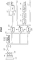
- the position detecting apparatus comprises a sensor 101 which detects a position read-on signals from a measuring scale 100.
- the read-on signals are picked up through a switch unit 102 as three-phase signals.
- the three-phase signals are analog signals whose phases are offset with each other by 120°.
- the analog signals are supplied to an A/D converter 104 through an amplifier 103.
- An output from the A/D converter 104 is supplied to an offset value calculator 105 wherein an offset value of the three-phase signals A, B and C are calculated by adding the signals A0, B0 and C0 and dividing the sum of them by 3.
- the calculated offset value is supplied to subtracters 106, 107 and 108. Further, the signals A0, B0 and C0 are supplied to the subtracters 106, 107 and 108, respectively.
- Each of the subtracters 106, 107 and 108 calculates a difference between the signal A0, B0, C0 and the offset value. These calculations at the subtracters 106, 107 and 108 correspond to a correction of the detected three-phase signals as to the offset value. If the offset value inputted to the subtracters 106, 107 and 108 takes a minus value, the substracters 106, 107 and 108 execute adding operation.
- output ends 113, 115 and 117 output signals A1, B1 and C1, respectively, from which the offset value has been eliminated.
- the output A1 of the subtracter 106 is supplied to a square calculator 109 wherein G 2 sin 2 ⁇ is generated.
- the generated value G 2 sin 2 ⁇ is outputted to an output end 114.
- the outputs B1 and C1 from the subtracters 107 and 108 are supplied to a subtracter 110 where the difference (B1-C1) is calculated.
- the output of the subtracter 110 is supplied to a square calculator 111 where (B1-C1)2 is obtained.
- the calculated value (B1-C1)2 is supplied to a divider 112 where (B1-C1) 2 /3 is obtained by dividing (B1-C1)2 by 3.
- the calculated value (B1-C1) 2 /3 is outputted to an output end 116.
- the divider 112 may be replaced by a multiplier which multiplies the value (B1-C1)2 with 1/3 (0.33).
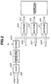
- the signal G 2 sin 2 ⁇ outputted to the output end 114 and the signal G 2 cos 2 ⁇ outputted to the output end 116 are supplied to input ends 210 and 202, respectively, as shown in Fig. 2.
- the output G2 of the adder 203 is inputted into a square-root calculator 204 wherein G is obtained by calculating a square-root of G2.
- the value G represents the above-mentioned gain and is supplied to a divider 205 wherein a gain ratio G0/G is obtained.
- One input end of each multiplier 209, 210, 211 receives the signal A1, B1, C1.
- Another input end of each multiplier 209, 210, 211 receives the gain ratio G/G0 from the divider 205.
- the multipliers 209, 210 and 211 outputs signals A2, B2 and C2 which have been corrected by the present gain. Therefore, it becomes possible to execute an accurate position detection based on the phase ⁇ of the signals.
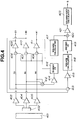
- the position detecting apparatus is an analog-signal processing type.
- a measuring scale 401 and a sensor 402 are positioned so as to be relatively movable, that is, one of them is installed at a fixed position, and the other one is installed at a movable object.
- the sensor 402 detects three-phase signals A0, B0 and C0 whose phases are shifted by 120° with each other.
- the three-phase signals A0, B0 and C0 are sent to amplifiers 403, 404 and 405, respectively, and their gains are adjusted (controlled).
- the output signals from the amplifier 403, 404 and 405 are added at an adder 412 to form a signal indicative of the sum ( A 0 + B 0 + C 0 ).
- the signal indicative of the sum is supplied to a divider 416 through an amplifier 414.
- the signal indicative of the sum ( A 0 + B 0 + C 0 ) can be represented by the sum 3D OFF of the respective offset values as shown by the equation (1). Therefore, by dividing the sum ( A 0 + B 0 + C 0 ) by 3 at the divider 414, the signal indicative of the offset value D OFF is derived.
- the signals A0, B0 and C0 outputted from the respective amplifiers 403, 404 and 405 are sent to subtracters 406, 407 and 408, respectively so that offset eliminated signals are obtained by the subtraction of the offset value D OFF of the divider 416 from the inputted signals A0, B0 and C0.
- Output signals from subtracters 406, 407 and 408 are inputted to amplifiers 409, 410 and 411, respectively, and offset eliminated signals A1, B1 and C1, from which offset has been eliminated, are outputted therefrom.
- the signal C1 from the amplifier 409 and the signal B1 from the amplifier 410 are inputted to a subtracter 413 where a difference signal (B1 - C1) is calculated and outputted.
- the signal outputted from the subtracter 413 is a signal from which an offset has been eliminated and which includes a value 3 Gcos ⁇ derived from the equation (2).
- the output signals C0 and B0 from the amplifiers 403 and 404 may be used instead of the output signals C1 and B1 from the amplifiers 409 and 410.
- a square calculating block 418 calculates the square of the signal 3 Gcos ⁇ and outputs a signal indicative of 3G 2 con 2 ⁇ .
- the output of the square calculating block 418 is supplied to a divider (or multiplier) 419 wherein the signal indicative of 3G 2 con 2 ⁇ is divided by 3 (or multiplied by 1/3), and a signal indicative of G 2 con 2 ⁇ is outputted.
- the obtained value G represents a gain and is a parameter relating to the amplitude of the respective three-phase signals A1, B1 and C1.
- Fig. 5 shows a circuit for executing a gain correction.
- the present gain G and the standard gain G0 are inputted to a divider 503 wherein the gain ratio G0/G is calculated.
- the output of the divider 503 is inputted to the respective multipliers 507, 508 and 509 where the signals indicative of C1, B1 and A1 is multiplied with the ratio G0/G, respectively, in order to correct the amplitudes of the signals indicative of C1, B1 and A1 according to the gain ratio.
- the corrected signals are supplied to the switches 513, 514 and 515 through amplifiers 510, 511 and 512, respectively. According to the sequential switching operation of the respective switches 515, 514 and 513, the signals are supplied to an A/D converter 516 where the inputted signals are converted into digital signals. Further, the converted digital signals are inputted to a later circuit 517 which has been used in a conventional position detecting apparatus.
- the standard gain G0 has been properly determined, it is further preferable to store the maximum value and the minimum value of the standard gain G0 at a previous turning-off of the electric source by means of EEPROM or NVRAM in order to be applicable to such a case that the offset values and gains with respect to the signals A, B and C are largely dispersed. Also, the maximum value and the minimum value read from the sensor at an initial setting period may be stored in a memory.
- a step S1 the respective input signals A, B and C are read-in from the sensor.
- the square root of G2 is calculated.
- a step S5 the gain amplitude is obtained by correcting the maximum amplitude of a previously stored value by the present gain G. That is, the calculation of the following equations is executed.
- G AOFF G(G Amax -G Amin )
- G BOFF G(G Bmax -G Bmin )
- G COFF G(G Cmax -G Cmin )
- the present maximum gain and minimum gain are calculated from the midpoints G Amid , G Bmid and G Cmid and the gain amplitudes G AOFF , G BOFF and G COFF . That is, the calculation of the following equations is executed.
- the position detection is accurately executed. Further, even if the gain is changed due to the thermal and/or machinery effect, the accurate detection is executed by correcting the obtained data.
Landscapes
- Physics & Mathematics (AREA)
- General Physics & Mathematics (AREA)
- Engineering & Computer Science (AREA)
- Power Engineering (AREA)
- Signal Processing (AREA)
- Transmission And Conversion Of Sensor Element Output (AREA)
- Measurement Of Length, Angles, Or The Like Using Electric Or Magnetic Means (AREA)
Applications Claiming Priority (2)
| Application Number | Priority Date | Filing Date | Title |
|---|---|---|---|
| JP237571/94 | 1994-09-30 | ||
| JP23757194A JP3312504B2 (ja) | 1994-09-30 | 1994-09-30 | 位置検出装置 |
Publications (2)
| Publication Number | Publication Date |
|---|---|
| EP0704679A1 true EP0704679A1 (de) | 1996-04-03 |
| EP0704679B1 EP0704679B1 (de) | 1998-06-03 |
Family
ID=17017294
Family Applications (1)
| Application Number | Title | Priority Date | Filing Date |
|---|---|---|---|
| EP95115434A Expired - Lifetime EP0704679B1 (de) | 1994-09-30 | 1995-09-29 | Vorrichtung zur Positionsdetektion |
Country Status (4)
| Country | Link |
|---|---|
| US (1) | US5663643A (de) |
| EP (1) | EP0704679B1 (de) |
| JP (1) | JP3312504B2 (de) |
| DE (1) | DE69502789T2 (de) |
Cited By (3)
| Publication number | Priority date | Publication date | Assignee | Title |
|---|---|---|---|---|
| WO2005050140A1 (en) * | 2003-11-18 | 2005-06-02 | Koninklijke Philips Electronics N.V. | Position determining |
| US6973399B1 (en) | 1999-03-30 | 2005-12-06 | Dr. Johannes Heidenhain Gmbh | Method and circuit for correcting periodic signals of an incremental position measuring system |
| DE19738528B4 (de) * | 1996-09-03 | 2007-02-08 | Sony Precision Technology Inc. | Vorrichtung und Verfahren zur Verschiebungsmessung |
Families Citing this family (7)
| Publication number | Priority date | Publication date | Assignee | Title |
|---|---|---|---|---|
| DE602004010672T2 (de) * | 2003-06-18 | 2008-04-30 | Nxp B.V. | Schaltungsanordnung und verfahren zur gewinnung eines ausgangssignals, sowie mit einer derartigen schaltungsanordnung ausgestattete drehzahlmessvorrichtung |
| JPWO2006043403A1 (ja) | 2004-10-20 | 2008-05-22 | 株式会社安川電機 | エンコーダ信号処理装置およびその信号処理方法 |
| WO2007055092A1 (ja) * | 2005-11-09 | 2007-05-18 | Kabushiki Kaisha Yaskawa Denki | エンコーダ信号処理装置 |
| JPWO2011111494A1 (ja) * | 2010-03-12 | 2013-06-27 | アルプス電気株式会社 | 磁気センサ及び磁気エンコーダ |
| JP2015017950A (ja) * | 2013-07-12 | 2015-01-29 | 株式会社東芝 | 位置検出装置および駆動システム |
| DE102014113289B4 (de) * | 2014-09-16 | 2016-04-28 | Helmholtz-Zentrum Berlin Für Materialien Und Energie Gmbh | Verfahren zur Bestimmung einer Position eines Objektes |
| JP2021006769A (ja) * | 2019-06-28 | 2021-01-21 | 三菱電機株式会社 | 回転角度検出装置 |
Citations (5)
| Publication number | Priority date | Publication date | Assignee | Title |
|---|---|---|---|---|
| JPS60114714A (ja) * | 1983-11-28 | 1985-06-21 | Sankyo Seiki Mfg Co Ltd | 磁気式エンコ−ダ− |
| DE3740544A1 (de) * | 1987-11-30 | 1989-06-08 | Neutron Mikroelektronik Gmbh | Einrichtung zur wandlung einer weg- oder winkelgroesse in eine elektrische inkrementale oder digitale groesse |
| DE4030946A1 (de) * | 1989-12-27 | 1991-10-10 | Gerfema Ges Fuer Rationalisier | Verfahren und schaltungsanordnung zur umformung sinusaehnlicher sensorsignale eines positionsmesssystems |
| DE9217004U1 (de) * | 1992-12-14 | 1993-02-18 | Siemens AG, 8000 München | Vorrichtung zum Ausgleich eines Fehlwinkels zwischen einem cosinus- und einem sinusförmigen, lageabhängigen Meßsignal bei einem Winkelgeber bzw. einem Linearmaßstab |
| EP0588549A2 (de) * | 1992-09-18 | 1994-03-23 | Sony Corporation | Verfahren zur Positionsermittlung |
Family Cites Families (1)
| Publication number | Priority date | Publication date | Assignee | Title |
|---|---|---|---|---|
| JPH05231807A (ja) * | 1992-02-18 | 1993-09-07 | Sony Corp | 位置検出器の異常監視装置 |
-
1994
- 1994-09-30 JP JP23757194A patent/JP3312504B2/ja not_active Expired - Fee Related
-
1995
- 1995-09-29 US US08/536,171 patent/US5663643A/en not_active Expired - Lifetime
- 1995-09-29 EP EP95115434A patent/EP0704679B1/de not_active Expired - Lifetime
- 1995-09-29 DE DE69502789T patent/DE69502789T2/de not_active Expired - Lifetime
Patent Citations (5)
| Publication number | Priority date | Publication date | Assignee | Title |
|---|---|---|---|---|
| JPS60114714A (ja) * | 1983-11-28 | 1985-06-21 | Sankyo Seiki Mfg Co Ltd | 磁気式エンコ−ダ− |
| DE3740544A1 (de) * | 1987-11-30 | 1989-06-08 | Neutron Mikroelektronik Gmbh | Einrichtung zur wandlung einer weg- oder winkelgroesse in eine elektrische inkrementale oder digitale groesse |
| DE4030946A1 (de) * | 1989-12-27 | 1991-10-10 | Gerfema Ges Fuer Rationalisier | Verfahren und schaltungsanordnung zur umformung sinusaehnlicher sensorsignale eines positionsmesssystems |
| EP0588549A2 (de) * | 1992-09-18 | 1994-03-23 | Sony Corporation | Verfahren zur Positionsermittlung |
| DE9217004U1 (de) * | 1992-12-14 | 1993-02-18 | Siemens AG, 8000 München | Vorrichtung zum Ausgleich eines Fehlwinkels zwischen einem cosinus- und einem sinusförmigen, lageabhängigen Meßsignal bei einem Winkelgeber bzw. einem Linearmaßstab |
Non-Patent Citations (1)
| Title |
|---|
| PATENT ABSTRACTS OF JAPAN vol. 009, no. 265 (P - 399) 23 October 1985 (1985-10-23) * |
Cited By (3)
| Publication number | Priority date | Publication date | Assignee | Title |
|---|---|---|---|---|
| DE19738528B4 (de) * | 1996-09-03 | 2007-02-08 | Sony Precision Technology Inc. | Vorrichtung und Verfahren zur Verschiebungsmessung |
| US6973399B1 (en) | 1999-03-30 | 2005-12-06 | Dr. Johannes Heidenhain Gmbh | Method and circuit for correcting periodic signals of an incremental position measuring system |
| WO2005050140A1 (en) * | 2003-11-18 | 2005-06-02 | Koninklijke Philips Electronics N.V. | Position determining |
Also Published As
| Publication number | Publication date |
|---|---|
| EP0704679B1 (de) | 1998-06-03 |
| US5663643A (en) | 1997-09-02 |
| DE69502789D1 (de) | 1998-07-09 |
| DE69502789T2 (de) | 1998-10-01 |
| JPH08101045A (ja) | 1996-04-16 |
| JP3312504B2 (ja) | 2002-08-12 |
Similar Documents
| Publication | Publication Date | Title |
|---|---|---|
| EP0708311B1 (de) | Verschiebungsmesseinrichtung | |
| EP0599175B1 (de) | Interpolationsgerät für Skalenanordnung | |
| US6534969B1 (en) | Offset-compensated angle measuring system | |
| EP2209213B1 (de) | RD-Wandler und Winkelerkennungsvorrichtung | |
| US6188341B1 (en) | Encoder interpolation circuit which corrects an interpolation angle between a received sine-wave encoder signal and a cosine-wave encoder signal | |
| EP0704679A1 (de) | Vorrichtung zur Positionsdetektion | |
| JP3372450B2 (ja) | エンコーダの出力信号処理装置 | |
| US4740660A (en) | Coordinate input apparatus | |
| JPH037968B2 (de) | ||
| JPH0591780A (ja) | 3相電動機の制御方法および装置 | |
| JPH08262073A (ja) | 力率の測定方法及び装置 | |
| CN110554345A (zh) | 一种电流传感器下线标定方法 | |
| US4534004A (en) | Apparatus and method for determining signal parameters of periodic square wave signals | |
| JP2801124B2 (ja) | トルクセンサの零点誤差の補正方法 | |
| KR100459127B1 (ko) | 모터의 상 전류 검출 장치 및 그 방법 | |
| US7443161B2 (en) | Method of determining angles | |
| KR20060101999A (ko) | 교류모터의 로터위치 감지장치의 감지신호 보상 방법 | |
| JP2806730B2 (ja) | トルクセンサの零点誤差の補正方法 | |
| KR100189937B1 (ko) | 정현파 신호를 사용한 회전각 추정 장치 및 방법 | |
| JPH0658769A (ja) | 信号処理方法及びそれを用いた変位検出装置 | |
| CN114487944B (zh) | 零增益温漂直流磁场测量方法 | |
| JPH05256638A (ja) | 誤差補正機能付き位置検出装置 | |
| JP7581693B2 (ja) | 電流センサ | |
| JP3318649B2 (ja) | 測定データ処理装置および方法 | |
| JPS60257314A (ja) | 非直線性補正装置 |
Legal Events
| Date | Code | Title | Description |
|---|---|---|---|
| PUAI | Public reference made under article 153(3) epc to a published international application that has entered the european phase |
Free format text: ORIGINAL CODE: 0009012 |
|
| 17P | Request for examination filed |
Effective date: 19950929 |
|
| AK | Designated contracting states |
Kind code of ref document: A1 Designated state(s): CH DE FR GB LI NL |
|
| 17Q | First examination report despatched |
Effective date: 19961104 |
|
| GRAG | Despatch of communication of intention to grant |
Free format text: ORIGINAL CODE: EPIDOS AGRA |
|
| RAP1 | Party data changed (applicant data changed or rights of an application transferred) |
Owner name: SONY PRECISION TECHNOLOGY INC. |
|
| GRAG | Despatch of communication of intention to grant |
Free format text: ORIGINAL CODE: EPIDOS AGRA |
|
| GRAH | Despatch of communication of intention to grant a patent |
Free format text: ORIGINAL CODE: EPIDOS IGRA |
|
| GRAH | Despatch of communication of intention to grant a patent |
Free format text: ORIGINAL CODE: EPIDOS IGRA |
|
| GRAA | (expected) grant |
Free format text: ORIGINAL CODE: 0009210 |
|
| AK | Designated contracting states |
Kind code of ref document: B1 Designated state(s): CH DE FR GB LI NL |
|
| REG | Reference to a national code |
Ref country code: CH Ref legal event code: NV Representative=s name: PATENTANWALTSBUERO JEAN HUNZIKER Ref country code: CH Ref legal event code: EP |
|
| REF | Corresponds to: |
Ref document number: 69502789 Country of ref document: DE Date of ref document: 19980709 |
|
| ET | Fr: translation filed | ||
| PLBE | No opposition filed within time limit |
Free format text: ORIGINAL CODE: 0009261 |
|
| STAA | Information on the status of an ep patent application or granted ep patent |
Free format text: STATUS: NO OPPOSITION FILED WITHIN TIME LIMIT |
|
| 26N | No opposition filed | ||
| REG | Reference to a national code |
Ref country code: GB Ref legal event code: IF02 |
|
| REG | Reference to a national code |
Ref country code: CH Ref legal event code: PUE Owner name: MAGNESCALE CO., LTD. Free format text: SONY PRECISION TECHNOLOGY INC.#9-17 NISHIGOTANDA 3-CHOME,#SHINAGAWA-KU TOKYO (JP) -TRANSFER TO- MAGNESCALE CO., LTD.#SHINAGAWA INTERCITY TOWER A-18F 2-15-1 KONAN#MINATU-KU TOKYO 108-6018 (JP) |
|
| REG | Reference to a national code |
Ref country code: NL Ref legal event code: SD Effective date: 20110630 |
|
| REG | Reference to a national code |
Ref country code: GB Ref legal event code: 732E Free format text: REGISTERED BETWEEN 20110728 AND 20110803 |
|
| REG | Reference to a national code |
Ref country code: DE Ref legal event code: R082 Ref document number: 69502789 Country of ref document: DE Representative=s name: GRUENECKER, KINKELDEY, STOCKMAIR & SCHWANHAEUS, DE |
|
| REG | Reference to a national code |
Ref country code: CH Ref legal event code: PUE Owner name: MORI SEIKO CO.,LTD., JP Free format text: FORMER OWNER: MAGNESCALE CO., LTD., JP |
|
| REG | Reference to a national code |
Ref country code: NL Ref legal event code: SD Effective date: 20130903 |
|
| REG | Reference to a national code |
Ref country code: DE Ref legal event code: R082 Ref document number: 69502789 Country of ref document: DE Representative=s name: GRUENECKER PATENT- UND RECHTSANWAELTE PARTG MB, DE Effective date: 20130806 Ref country code: DE Ref legal event code: R082 Ref document number: 69502789 Country of ref document: DE Representative=s name: GRUENECKER, KINKELDEY, STOCKMAIR & SCHWANHAEUS, DE Effective date: 20130806 Ref country code: DE Ref legal event code: R081 Ref document number: 69502789 Country of ref document: DE Owner name: MORI SEIKI CO., LTD., YAMATOKORIYAMA-SHI, JP Free format text: FORMER OWNER: MAGNESCALE CO., LTD., TOKYO, JP Effective date: 20130806 Ref country code: DE Ref legal event code: R081 Ref document number: 69502789 Country of ref document: DE Owner name: MORI SEIKI CO., LTD., JP Free format text: FORMER OWNER: MAGNESCALE CO., LTD., TOKYO, JP Effective date: 20130806 |
|
| REG | Reference to a national code |
Ref country code: GB Ref legal event code: 732E Free format text: REGISTERED BETWEEN 20130926 AND 20131002 |
|
| REG | Reference to a national code |
Ref country code: FR Ref legal event code: TP Owner name: MORI SEIKI CO., LTD., JP Effective date: 20130924 |
|
| PGFP | Annual fee paid to national office [announced via postgrant information from national office to epo] |
Ref country code: NL Payment date: 20130918 Year of fee payment: 19 Ref country code: CH Payment date: 20130919 Year of fee payment: 19 Ref country code: DE Payment date: 20130919 Year of fee payment: 19 |
|
| REG | Reference to a national code |
Ref country code: CH Ref legal event code: PK Free format text: BERICHTIGUNG INHABER |
|
| PGFP | Annual fee paid to national office [announced via postgrant information from national office to epo] |
Ref country code: FR Payment date: 20130919 Year of fee payment: 19 Ref country code: GB Payment date: 20130919 Year of fee payment: 19 |
|
| REG | Reference to a national code |
Ref country code: DE Ref legal event code: R119 Ref document number: 69502789 Country of ref document: DE |
|
| REG | Reference to a national code |
Ref country code: CH Ref legal event code: PL |
|
| GBPC | Gb: european patent ceased through non-payment of renewal fee |
Effective date: 20140929 |
|
| REG | Reference to a national code |
Ref country code: FR Ref legal event code: ST Effective date: 20150529 |
|
| PG25 | Lapsed in a contracting state [announced via postgrant information from national office to epo] |
Ref country code: NL Free format text: LAPSE BECAUSE OF NON-PAYMENT OF DUE FEES Effective date: 20150401 |
|
| PG25 | Lapsed in a contracting state [announced via postgrant information from national office to epo] |
Ref country code: DE Free format text: LAPSE BECAUSE OF NON-PAYMENT OF DUE FEES Effective date: 20150401 Ref country code: LI Free format text: LAPSE BECAUSE OF NON-PAYMENT OF DUE FEES Effective date: 20140930 Ref country code: GB Free format text: LAPSE BECAUSE OF NON-PAYMENT OF DUE FEES Effective date: 20140929 Ref country code: CH Free format text: LAPSE BECAUSE OF NON-PAYMENT OF DUE FEES Effective date: 20140930 |
|
| PG25 | Lapsed in a contracting state [announced via postgrant information from national office to epo] |
Ref country code: FR Free format text: LAPSE BECAUSE OF NON-PAYMENT OF DUE FEES Effective date: 20140930 |