EP0704706B1 - A diagnostic system for a capacitive sensor - Google Patents
A diagnostic system for a capacitive sensor Download PDFInfo
- Publication number
- EP0704706B1 EP0704706B1 EP95115291A EP95115291A EP0704706B1 EP 0704706 B1 EP0704706 B1 EP 0704706B1 EP 95115291 A EP95115291 A EP 95115291A EP 95115291 A EP95115291 A EP 95115291A EP 0704706 B1 EP0704706 B1 EP 0704706B1
- Authority
- EP
- European Patent Office
- Prior art keywords
- sensor
- sens
- osc
- riv
- circuit
- Prior art date
- Legal status (The legal status is an assumption and is not a legal conclusion. Google has not performed a legal analysis and makes no representation as to the accuracy of the status listed.)
- Expired - Lifetime
Links
- 238000003745 diagnosis Methods 0.000 claims description 7
- 238000001514 detection method Methods 0.000 claims description 6
- 230000006978 adaptation Effects 0.000 claims description 5
- 230000010355 oscillation Effects 0.000 claims description 5
- 230000000737 periodic effect Effects 0.000 claims description 3
- 230000003213 activating effect Effects 0.000 claims 1
- 230000001419 dependent effect Effects 0.000 claims 1
- 238000005474 detonation Methods 0.000 description 7
- 238000005259 measurement Methods 0.000 description 5
- 238000000034 method Methods 0.000 description 5
- 238000010586 diagram Methods 0.000 description 4
- 230000010354 integration Effects 0.000 description 3
- 230000004075 alteration Effects 0.000 description 2
- 230000002238 attenuated effect Effects 0.000 description 2
- 230000003071 parasitic effect Effects 0.000 description 2
- 230000007704 transition Effects 0.000 description 2
- 230000001133 acceleration Effects 0.000 description 1
- 230000003321 amplification Effects 0.000 description 1
- 230000015572 biosynthetic process Effects 0.000 description 1
- 238000004364 calculation method Methods 0.000 description 1
- 238000006243 chemical reaction Methods 0.000 description 1
- 238000002485 combustion reaction Methods 0.000 description 1
- 238000010276 construction Methods 0.000 description 1
- 230000002596 correlated effect Effects 0.000 description 1
- 238000011161 development Methods 0.000 description 1
- 238000007599 discharging Methods 0.000 description 1
- 238000006073 displacement reaction Methods 0.000 description 1
- 230000000694 effects Effects 0.000 description 1
- 238000005516 engineering process Methods 0.000 description 1
- 238000001914 filtration Methods 0.000 description 1
- 238000004519 manufacturing process Methods 0.000 description 1
- 238000012544 monitoring process Methods 0.000 description 1
- 238000003199 nucleic acid amplification method Methods 0.000 description 1
- 230000001105 regulatory effect Effects 0.000 description 1
- 230000035945 sensitivity Effects 0.000 description 1
- 238000003786 synthesis reaction Methods 0.000 description 1
- 238000012546 transfer Methods 0.000 description 1
Images


Classifications
-
- G—PHYSICS
- G01—MEASURING; TESTING
- G01R—MEASURING ELECTRIC VARIABLES; MEASURING MAGNETIC VARIABLES
- G01R31/00—Arrangements for testing electric properties; Arrangements for locating electric faults; Arrangements for electrical testing characterised by what is being tested not provided for elsewhere
- G01R31/28—Testing of electronic circuits, e.g. by signal tracer
- G01R31/282—Testing of electronic circuits specially adapted for particular applications not provided for elsewhere
- G01R31/2829—Testing of circuits in sensor or actuator systems
-
- G—PHYSICS
- G01—MEASURING; TESTING
- G01P—MEASURING LINEAR OR ANGULAR SPEED, ACCELERATION, DECELERATION, OR SHOCK; INDICATING PRESENCE, ABSENCE, OR DIRECTION, OF MOVEMENT
- G01P21/00—Testing or calibrating of apparatus or devices covered by the preceding groups
Definitions
- the present invention relates in general to a diagnostic system for a capacitive sensor, of the kind defined in the preamble of claim 1.
- the object of the present invention is that of providing a diagnostic system which permits all the above-indicated problems to be resolved in a satisfactory manner.
- the system according to the present invention has been developed to diagnose the state of the input connection of a device for detecting detonation (also called knock) which utilises a piezoelectric accelerometric sensor of capacitive type.
- the system solves the following problem: given a system for the detection of detonation, find a method which succeeds in diagnosing the following conditions at the input of the device:
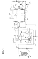
- the system utilises an oscillator which, during diagnosis, is connected between the sensor and a detection device or detector (see in this connection the block diagram of Figure 1).
- the frequency of the oscillator depends on the capacitance present at the input terminal of the system itself. If the sensor is connected the oscillator frequency falls within the detector band and therefore at the output of the detector there will be a signal greater than a discrimination threshold; if the sensor is detached the oscillator frequency will be so high as to fall outside the detector band and therefore will have at its output a signal less than the discrimination threshold, in the limit a zero threshold.
- the oscillator (of digital type) remains clamped at low or high logic level respectively, whilst the output of the detector will in both cases be less than the discrimination threshold, in the limit zero.
- the system is general and can be applied to detonation detection devices having one or several tuning channels.
- the system will now be described in more detail in the case of a two-channel device.
- the diagnostic system according to the invention is based on a block diagram of the type shown in Figure 1.
- the diagnostic system DIAGNOST is interposed between a sensor SENS and a detector circuit RIV during the diagnostic phase, which is activated by means of a digital "high" signal DIA.
- the detector circuit RIV comprises an interface amplifier INPUT connected to the input INA of the detector circuit RIV.
- the output of the interface amplifier INPUT is connected to two tuning channels CHA and CHB.
- the outputs of the two tuning channels CHA and CHB join together at a summing node SUM which in turn is connected to an integrator INT with an integration time Tg, the output of which is connected to the output OUT of the detector circuit RIV.
- Each of the two tuning channels CHA, CHB is in turn composed of a band pass filter BPF and a double half wave rectifier FWR.
- the diagnostic system DIAGNOST is, on the other hand, constituted by the following fundamental blocks:
- the charge present at an input IN of the system DIAGNOST is supposed to be formed by a capacitance C c , which represents the connection of the cabling and possible parasitic capacitances on the input node IN, and the sensor SENS.
- the sensor SENS is schematically represented by the parallel connection of a capacitance C s and a resistance R s , and by a voltage generator V s which converts the acceleration into voltage.
- the system DIAGNOST is based on the fact that, in the diagnostic configuration, the detector RIV acts on the oscillator signal OSC, the frequency of which depends on the equivalent capacitance present at the input IN, thereby determining an output signal from which it is possible to diagnose the connected, detached or short circuited condition of the sensor SENS as will be explained herein below.
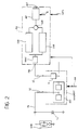
- the periodic signal which supplies the input interface INPUT of the detector RIV, see Figure 2 is a square wave with a predetermined duty cycle (in general 50%), with an amplitude such as to exploit the maximum available dynamic range of the input interface INPUT and the amplifiers.
- the detector RIV is assumed tuned to the channels CHA and CHB at respective central frequencies F A and F B , gains G A and G B and quality factors Q A and Q B ; in general the modulus of the transfer function (hereinafter called FDT for brevity) of the band pass filters BPF will be considered of the type:
- the output of the filters BPF produces only the first harmonic of the square wave signal present at the input (output of the oscillator OSC); since the upper harmonics are generally above the maximum frequency which can be handled.
- V I (F o ,t) V osc K a1 [M A (F o )+M B (F o )] sin(2 ⁇ F o t)
- V osc K a1 M A,B (F o ) where the factor 2/ ⁇ takes account of the mean of the rectified sinusoid and M A,B (F o ) is the sum of the moduli of the FDT of the channels CHA and CHB at the frequency of the oscillator OSC.
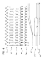
- the oscillation frequency falls in an interval lying between f a1 and f b1 , such that the input signal of the integrator INT is attenuated, at most, by a factor 2a s .
- the oscillation frequency is so high, greater than f c , that the signal is attenuated at least by a factor a c ⁇ 2a s .
- the different attenuation in the two cases establishes the discrimination margin between the sensor SENS connected and detached as will explained hereinbelow.
- the discrimination factor is at least 6dB if the relations (18) and (22) are satisfied and the filters (or the filter) BPF are at least of the second order.
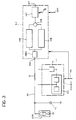
- the oscillator OSC is formed by transistors Q1-Q6, an amplifier O1, a comparator O2, resistors R DIA , R1, R2 and R3, MOS type switches S7, S8 and S9 and invertors I2, I3 and I4.
- the switching block is implemented by the invertors I1 and the MOS switches S1, S2, S3, S4 and S5 controlled by the signal DIA.
- Two invertors I3 and I4 at the output of a comparator O2 provide the square wave digital signal of the oscillator OSC.
- the shifter K which provides the analogue signal of the oscillator OSC which supplies the detonation detector RIV is constituted by an operational amplifier O3, resistors RA1, RA2, RA3 and MOS switch S6. These components, as will be explained hereinbelow, form a variable gain amplifier the gain of which varies as a function of the signal DIA, and therefore, implement the oscillating signal adaptation constant K. This variable gain amplifier can replace the input interface INPUT of the detector RIV.
- the diagnostic system DIAGNOST is isolated from the detector RIV (except for the closure resistance of the switches S3 and S5 and the opening of the switches S1, S2 and S4), and the input load is connected directly to the interface amplifier INPUT.
- the diagnostic system DIAGNOST is interposed between the input load and the input INA of the detector RIV.
- the individual blocks will now be analysed. Oscillator and switches.
- the high level of the signal DIA enables diagnosis by closing the switches S1, S2 and S4 and opening the switches S3 and S5; the function of the switch S4 is to prevent cross-talk between the connection of the sensor SENS and the input INA of the detector RIV.
- the oscillator OSC is activated by opening the reset switch S7 by means of the invertor 12. In these conditions the input capacity is connected to the non-inverting input of the comparator O2 the output of which is connected to the input of the amplifier O3 via the resistor RA1 and the invertors I3 and I4.
- the high level of the signal DIA enables a logic circuit LOG.
- This circuit LOG counts n transitions of the oscillating signal taken from the output of the invertor I4 and produces at its output two logic signals OD1 and OD2 which partially diagnose the charge state of the input.
- Figure 7 there is shown a possible implementation of the logic circuit LOG in the particular case of counting two transitions of the oscillating signal by the use of two D-type flip-flops, FF1, FF2.
- OD1 OD2 Condition 1 X i) Input load purely capacitive with oscillator OSC operating. 0 1 ii) Oscillator OSC clamped at HIGH logic level: condition of short circuit to supply. 0 0 iii) Oscillator OSC clamped at LOW logic level: condition of short circuit to ground.
- the logic conditions of the table can be correlated with the output analogue voltage of the system to obtain the complete diagnosis of the state of the input load state.
- the value R icca thus discriminates between the partial short circuit resistance to the supply V cc .
- the system described here has been developed in particular for diagnosing the state of the load at the input of a detonation detection circuit, applicable in engine control computers which utilise accelerometric sensors of capacitive type as detonation transducer sensors.
- the system is of a general type and can be applied to systems with one or more detection channels as long as they operate a frequency-voltage conversion with band pass filtering.
Landscapes
- Physics & Mathematics (AREA)
- General Physics & Mathematics (AREA)
- Electromagnetism (AREA)
- Engineering & Computer Science (AREA)
- General Engineering & Computer Science (AREA)
- Measurement Of Resistance Or Impedance (AREA)
- Testing Of Short-Circuits, Discontinuities, Leakage, Or Incorrect Line Connections (AREA)
Applications Claiming Priority (2)
| Application Number | Priority Date | Filing Date | Title |
|---|---|---|---|
| ITTO940764 | 1994-09-30 | ||
| IT94TO000764A IT1268099B1 (it) | 1994-09-30 | 1994-09-30 | Sistema di diagnosi per un sensore di tipo capacitivo. |
Publications (2)
| Publication Number | Publication Date |
|---|---|
| EP0704706A1 EP0704706A1 (en) | 1996-04-03 |
| EP0704706B1 true EP0704706B1 (en) | 1999-06-30 |
Family
ID=11412793
Family Applications (1)
| Application Number | Title | Priority Date | Filing Date |
|---|---|---|---|
| EP95115291A Expired - Lifetime EP0704706B1 (en) | 1994-09-30 | 1995-09-28 | A diagnostic system for a capacitive sensor |
Country Status (4)
| Country | Link |
|---|---|
| EP (1) | EP0704706B1 (it) |
| DE (1) | DE69510514T2 (it) |
| ES (1) | ES2135640T3 (it) |
| IT (1) | IT1268099B1 (it) |
Cited By (1)
| Publication number | Priority date | Publication date | Assignee | Title |
|---|---|---|---|---|
| US9791494B2 (en) | 2012-01-20 | 2017-10-17 | Lear Corporation | Apparatus and method for diagnostics of a capacitive sensor |
Families Citing this family (5)
| Publication number | Priority date | Publication date | Assignee | Title |
|---|---|---|---|---|
| DE19739903A1 (de) * | 1997-09-11 | 1999-04-01 | Bosch Gmbh Robert | Sensorvorrichtung |
| CA2390176A1 (en) * | 1999-11-03 | 2001-05-10 | Med-Dev Limited | Method and apparatus for testing a capacitive sensor |
| CN101669019B (zh) | 2007-04-06 | 2013-11-20 | 飞思卡尔半导体公司 | 与电容式传感器的诊断有关的改进 |
| US10260983B2 (en) | 2014-01-20 | 2019-04-16 | Lear Corporation | Apparatus and method for diagnostics of a capacitive sensor with plausibility check |
| CN116401596B (zh) * | 2023-06-08 | 2023-08-22 | 哈尔滨工业大学(威海) | 基于深度指数激励网络的早期故障诊断方法 |
Family Cites Families (5)
| Publication number | Priority date | Publication date | Assignee | Title |
|---|---|---|---|---|
| DE3235660A1 (de) * | 1982-09-27 | 1984-03-29 | Siemens AG, 1000 Berlin und 8000 München | Schaltungsanordnung zur ueberwachung eines elektrischen messfuehlers auf unterbrechung und ueberbrueckung |
| DE3627241A1 (de) * | 1986-08-12 | 1988-02-18 | Bosch Gmbh Robert | Schaltung und verfahren zur ueberpruefung elektronischer sensoren |
| GB8927927D0 (en) * | 1989-12-11 | 1990-02-14 | Kellett Michael A | Transducers and associated control circuits |
| GB2253487B (en) * | 1991-03-07 | 1994-08-03 | Rover Group | A method of detecting malfunction of a piezoelectric sensor |
| US5421191A (en) * | 1993-03-08 | 1995-06-06 | Chrysler Corporation | Knock sensor diagnostic system |
-
1994
- 1994-09-30 IT IT94TO000764A patent/IT1268099B1/it active IP Right Grant
-
1995
- 1995-09-28 EP EP95115291A patent/EP0704706B1/en not_active Expired - Lifetime
- 1995-09-28 ES ES95115291T patent/ES2135640T3/es not_active Expired - Lifetime
- 1995-09-28 DE DE69510514T patent/DE69510514T2/de not_active Expired - Fee Related
Cited By (1)
| Publication number | Priority date | Publication date | Assignee | Title |
|---|---|---|---|---|
| US9791494B2 (en) | 2012-01-20 | 2017-10-17 | Lear Corporation | Apparatus and method for diagnostics of a capacitive sensor |
Also Published As
| Publication number | Publication date |
|---|---|
| DE69510514T2 (de) | 1999-10-28 |
| DE69510514D1 (de) | 1999-08-05 |
| EP0704706A1 (en) | 1996-04-03 |
| ITTO940764A0 (it) | 1994-09-30 |
| IT1268099B1 (it) | 1997-02-20 |
| ES2135640T3 (es) | 1999-11-01 |
| ITTO940764A1 (it) | 1996-03-30 |
Similar Documents
| Publication | Publication Date | Title |
|---|---|---|
| US6703920B2 (en) | Device and method for contactless transmission of power or data | |
| US4277758A (en) | Ultrasonic wave generating apparatus with voltage-controlled filter | |
| US5895848A (en) | Apparatus and method for level sensing in a container | |
| US5461383A (en) | Wideband microwave detector | |
| US20030151930A1 (en) | Inductive contactless power transmitter | |
| EP0704706B1 (en) | A diagnostic system for a capacitive sensor | |
| US5637798A (en) | Circuit arrangement for evaluating an acceleration sensor signal | |
| US6628123B2 (en) | Method for controlling a transducer device in level sensors and device for carrying out such a method | |
| US6429571B2 (en) | Method to control piezoelectric drives | |
| US5796180A (en) | Device for transmitting data or energy | |
| KR100367543B1 (ko) | 가속감응센서를가지는전자장치 | |
| JPH0628230Y2 (ja) | 超音波振動子の振動制御装置 | |
| US7292021B2 (en) | Anomaly detector for vibratory angular rate sensor | |
| US5428997A (en) | Method of and device for fluid surface detection using an ultrasonic transducer | |
| WO1991013363A2 (en) | Signal conditioning circuit | |
| US5333489A (en) | Circuit arrangement to detect knocking | |
| JPH06505805A (ja) | 内燃機関のノッキング検出装置 | |
| JPH0775700B2 (ja) | 固有共振振動に対する機械振動系の自励振回路装置 | |
| JP2513329B2 (ja) | 周波数変調波受信装置 | |
| JP3640321B2 (ja) | 磁気的検知装置 | |
| JPS5922912B2 (ja) | 物体検出装置 | |
| GB2314438A (en) | Anti-theft system for a motor vehicle | |
| JPH02202799A (ja) | 超音波発生装置 | |
| SU809479A1 (ru) | Частотный дискриминатор | |
| JPH0412398Y2 (it) |
Legal Events
| Date | Code | Title | Description |
|---|---|---|---|
| PUAI | Public reference made under article 153(3) epc to a published international application that has entered the european phase |
Free format text: ORIGINAL CODE: 0009012 |
|
| AK | Designated contracting states |
Kind code of ref document: A1 Designated state(s): DE ES FR GB SE |
|
| 17P | Request for examination filed |
Effective date: 19960323 |
|
| 17Q | First examination report despatched |
Effective date: 19971203 |
|
| GRAG | Despatch of communication of intention to grant |
Free format text: ORIGINAL CODE: EPIDOS AGRA |
|
| GRAG | Despatch of communication of intention to grant |
Free format text: ORIGINAL CODE: EPIDOS AGRA |
|
| GRAH | Despatch of communication of intention to grant a patent |
Free format text: ORIGINAL CODE: EPIDOS IGRA |
|
| GRAH | Despatch of communication of intention to grant a patent |
Free format text: ORIGINAL CODE: EPIDOS IGRA |
|
| GRAA | (expected) grant |
Free format text: ORIGINAL CODE: 0009210 |
|
| AK | Designated contracting states |
Kind code of ref document: B1 Designated state(s): DE ES FR GB SE |
|
| REF | Corresponds to: |
Ref document number: 69510514 Country of ref document: DE Date of ref document: 19990805 |
|
| ET | Fr: translation filed | ||
| REG | Reference to a national code |
Ref country code: ES Ref legal event code: FG2A Ref document number: 2135640 Country of ref document: ES Kind code of ref document: T3 |
|
| PLBE | No opposition filed within time limit |
Free format text: ORIGINAL CODE: 0009261 |
|
| STAA | Information on the status of an ep patent application or granted ep patent |
Free format text: STATUS: NO OPPOSITION FILED WITHIN TIME LIMIT |
|
| 26N | No opposition filed | ||
| REG | Reference to a national code |
Ref country code: GB Ref legal event code: IF02 |
|
| PGFP | Annual fee paid to national office [announced via postgrant information from national office to epo] |
Ref country code: SE Payment date: 20020731 Year of fee payment: 8 |
|
| PGFP | Annual fee paid to national office [announced via postgrant information from national office to epo] |
Ref country code: ES Payment date: 20020802 Year of fee payment: 8 |
|
| PGFP | Annual fee paid to national office [announced via postgrant information from national office to epo] |
Ref country code: GB Payment date: 20020815 Year of fee payment: 8 |
|
| PGFP | Annual fee paid to national office [announced via postgrant information from national office to epo] |
Ref country code: DE Payment date: 20020822 Year of fee payment: 8 |
|
| PGFP | Annual fee paid to national office [announced via postgrant information from national office to epo] |
Ref country code: FR Payment date: 20020930 Year of fee payment: 8 |
|
| PG25 | Lapsed in a contracting state [announced via postgrant information from national office to epo] |
Ref country code: GB Free format text: LAPSE BECAUSE OF NON-PAYMENT OF DUE FEES Effective date: 20030928 |
|
| PG25 | Lapsed in a contracting state [announced via postgrant information from national office to epo] |
Ref country code: SE Free format text: LAPSE BECAUSE OF NON-PAYMENT OF DUE FEES Effective date: 20030929 Ref country code: ES Free format text: LAPSE BECAUSE OF NON-PAYMENT OF DUE FEES Effective date: 20030929 |
|
| PG25 | Lapsed in a contracting state [announced via postgrant information from national office to epo] |
Ref country code: DE Free format text: LAPSE BECAUSE OF NON-PAYMENT OF DUE FEES Effective date: 20040401 |
|
| EUG | Se: european patent has lapsed | ||
| GBPC | Gb: european patent ceased through non-payment of renewal fee |
Effective date: 20030928 |
|
| PG25 | Lapsed in a contracting state [announced via postgrant information from national office to epo] |
Ref country code: FR Free format text: LAPSE BECAUSE OF NON-PAYMENT OF DUE FEES Effective date: 20040528 |
|
| REG | Reference to a national code |
Ref country code: FR Ref legal event code: ST |
|
| REG | Reference to a national code |
Ref country code: ES Ref legal event code: FD2A Effective date: 20030929 |