EP0704800A2 - Dispositif de mémoire à semi-conducteur avec circuit de génération d'un signal de sélection d'une ligne de données redondante - Google Patents
Dispositif de mémoire à semi-conducteur avec circuit de génération d'un signal de sélection d'une ligne de données redondante Download PDFInfo
- Publication number
- EP0704800A2 EP0704800A2 EP95115350A EP95115350A EP0704800A2 EP 0704800 A2 EP0704800 A2 EP 0704800A2 EP 95115350 A EP95115350 A EP 95115350A EP 95115350 A EP95115350 A EP 95115350A EP 0704800 A2 EP0704800 A2 EP 0704800A2
- Authority
- EP
- European Patent Office
- Prior art keywords
- address
- level
- node
- bit line
- redundant bit
- Prior art date
- Legal status (The legal status is an assumption and is not a legal conclusion. Google has not performed a legal analysis and makes no representation as to the accuracy of the status listed.)
- Withdrawn
Links
- 239000004065 semiconductor Substances 0.000 title claims abstract description 25
- 230000004044 response Effects 0.000 claims abstract description 13
- 230000008859 change Effects 0.000 claims abstract description 9
- 230000015572 biosynthetic process Effects 0.000 claims 1
- 230000015654 memory Effects 0.000 description 19
- 238000010586 diagram Methods 0.000 description 5
- 101150070189 CIN3 gene Proteins 0.000 description 4
- 239000000872 buffer Substances 0.000 description 4
- 230000007704 transition Effects 0.000 description 4
- 101100286980 Daucus carota INV2 gene Proteins 0.000 description 2
- 101100397045 Xenopus laevis invs-b gene Proteins 0.000 description 2
- 230000002411 adverse Effects 0.000 description 2
- 230000008901 benefit Effects 0.000 description 2
- 238000012986 modification Methods 0.000 description 2
- 230000004048 modification Effects 0.000 description 2
- 101150110971 CIN7 gene Proteins 0.000 description 1
- 101100508840 Daucus carota INV3 gene Proteins 0.000 description 1
- 101150110298 INV1 gene Proteins 0.000 description 1
- 101100397044 Xenopus laevis invs-a gene Proteins 0.000 description 1
- 238000007796 conventional method Methods 0.000 description 1
- 230000003247 decreasing effect Effects 0.000 description 1
- 230000007547 defect Effects 0.000 description 1
- 230000003111 delayed effect Effects 0.000 description 1
- 230000000694 effects Effects 0.000 description 1
- 230000006870 function Effects 0.000 description 1
- 238000004519 manufacturing process Methods 0.000 description 1
- 230000002035 prolonged effect Effects 0.000 description 1
- 238000009966 trimming Methods 0.000 description 1
Images


Classifications
-
- G—PHYSICS
- G11—INFORMATION STORAGE
- G11C—STATIC STORES
- G11C29/00—Checking stores for correct operation ; Subsequent repair; Testing stores during standby or offline operation
-
- G—PHYSICS
- G11—INFORMATION STORAGE
- G11C—STATIC STORES
- G11C29/00—Checking stores for correct operation ; Subsequent repair; Testing stores during standby or offline operation
- G11C29/70—Masking faults in memories by using spares or by reconfiguring
- G11C29/78—Masking faults in memories by using spares or by reconfiguring using programmable devices
- G11C29/84—Masking faults in memories by using spares or by reconfiguring using programmable devices with improved access time or stability
Definitions
- the present invention relates to a semiconductor memory including a redundant bit line, more specifically, to a redundant bit line selection signal generating circuit for selecting a redundant bit line.
- semiconductor memories are highly integrated. Therefore, it is very difficult to manufacture semiconductor memory devices, all of which memory cells are operable under normal conditions.
- semiconductor memories contain redundant memory cells, and faulty memory cells founded by memory checks are replaced by these redundant memory cells so as to improve a yield.
- faulty memory cells are replaced by redundant memory cells in unit of row, or column as redundant structures.
- a selection signal YR2 becomes an active level (namely, low level)
- a column decoder (not shown) selects a redundant bit line, and also prohibits an access to a bit line where a faulty memory cell is present.
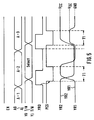
- External address signals A0 to Aj are supplied to address buffers 10 to 1j respectively every 1 bit.
- Each of address buffers produces column address signals Y0T to YjT corresponding to the 1-bit inputted address signals, respectively, and also produces address transition sensing signals ATD0 to ATDj when the inputted address signal is changed.
- address transition sensing signals ATD0 to ATDj when the external address signals A0 to Aj are changed, any one of the address transition sensing signals ATD0 to ATDj is produced.
- An ATD signal detecting circuit 2 detects that any one of the address transition sensing signals ATD0 to ATDj is produced to thereby generate a sensing signal YRD having a predetermined pulse width.
- the sensing signal YRD is inverted by an inverter INV2, and the inverted sensing signal is supplied as a precharge signal YRDB to a gate of a P-channel transistor P1.
- the P-channel transistor P1 is provided between a power source terminal V cc and a node YR1.
- An N-channel transistor N1 is provided between the node YR1 and a ground source GND, and an enable signal EN is supplied via an inverter INV3 to a gate of this N-channel transistor N1.
- Selecting circuits 30 to 3j are connected to the node YR1, to which corresponding column address signals Y0T to YjT are supplied.
- an N-channel transistor N2 series-connected with a fuse F1 and another N-channel transistor N3 series-connected with another fuse N2 are provided between the node YR1 and the ground source GND, respectively.
- the column address signal (for example, Y0T) is supplied to a gate of the transistor N2, and this column address signal is inverted by the inverter INV1 into a signal Y0N which will then be supplied to a gate of the transistor N3.
- an address of a faulty bit line is written into the selecting circuits 30 to 3j in order to replace the faulty bit line connected to this memory cell with a redundant bit line.
- any one of the fuses F1 and F2 provided in the selecting circuit is cut away by the laser trimming step in correspondence with the address of the faulty bit line.
- Such a fuse is cut away which is connected to the transistor that becomes conductive when the address of the faulty bit line is applied.
- a potential at the node YR1 is inverted by an inverter INV4, and then the inverted potential is outputted as a selection signal YR2.
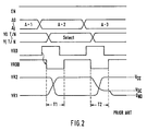
- Fig. 2 represents operation waveforms in the case that the address signals A0 to Aj are changed into A-1, A-2, A-3, and A-2 corresponds to an address of a faulty bit line.
- the transistor N1 Since the enable signal is at the high level during the read/write operations, the transistor N1 is under OFF state.
- the address signal becomes A-1, at least one of these selection circuits 30 to 3j forms the current path between the ground source and the node YR1, so that the potential level at the node YR1 is equal to the ground potential, and the selection signal YR2 becomes the high level (i.e., inactive level).
- the ATD signal detecting circuit 2 when the address signal is changed into A-2, at least one of address transition sensing signals ATD0 to ATDj is produced, and the ATD signal detecting circuit 2 generates the sensing signal YRD having a predetermined pulse width.
- the sensing signal YRD is inverted by the inverter INV2 and the inverted sensing signal is supplied as the precharge signal YRDB to the gate of the P-channel transistor P1.
- the transistor P1 is brought into the ON state for a time period (T1) during which this precharge signal YRDB is at the low level.
- the transistor P1 charges the node YR1 to V cc and causes the selection signal YR2 to become the low level (active level).
- the precharge signal YRDB is supplied to the gate of the P-channel transistor P1, so that the P-channel transistor P1 is under ON state during a time period of T2.
- the address signal A-3 is not the address of the faulty bit line
- at least one of the selection circuits 30 to 3j forms the current path between the ground source and the node YR1.
- the level at the node YR1 is lowered from V cc to V DC , so that the selection signal YR2 becomes the high level.
- the conductive resistance value R N , and the resistance value R F are varied by the quantities of the N-channel type transistors under conducting state and of the fuses. These resistance values are decreased when the quantities of paired sets of the series-connected fuse F1/transistor N2 and fuse F2/transistor N3 are increased.
- the condition under which the DC level V DC becomes the highest level when redundancy is unused corresponds to such a case that there is only one paired set of either the fuse F1/transistor N2 under conducting state or the fuse F2/transistor N3 under conducting state.
- the potential level at the node YR1 is varied from the power source level V cc to the DC level V DC corresponding to the intermediate potential.
- the time period during which this potential level at the node YR1 becomes lower than the threshold voltage of the inverter INV4 and the selection signal YR2 becomes the high level may greatly cause a problem in the DC level V DC .
- the stray capacitance of the node YR1 is increased since semiconductor memory devices are highly integrated and the quantity of selection circuits connected to this node YR1, namely a total number of fuses is increased.
- the current capability of the precharging transistor P1 must be increased.
- the current capabilities of the transistors N2 and N3 employed in the selection circuit 3 should also be increased in view of the above-described equations (1) and (2).
- the entire circuit area of semiconductor memory device should be increased.
- an object of the present invention is to provide a semiconductor memory device capable of resetting a redundant bit line selection signal at high speed when an address signal is changed from a selective condition of a redundant bit line into a non-selective condition.
- a semiconductor device for detecting that an input address is an address to be converted into a redundant bit line to cause a redundant bit line selection signal to become an active level is comprised of a control signal generating circuit for generating a control signal whose level is changed from a first level to a second level in synchronism with the change of the input address, and whose level becomes said first level after a predetermined time has elapsed, a charge circuit for electically connecting a first power source terminal with a node when control signal is at first level, and for electrically connecting the node with a second power source terminal when control signal is at second level, selecting means for electrically connecting the node with the second power source terminal when the input address corresponds to any address other than the address to be converted into said redundant bit, and for prohibiting the electric connection made between the node and the second power source terminal when input address corresponds to the address to be converted into said redundant bit, and storage means for storing therein data corresponding to the level of the node when control signal is at the first level and for producing the redundant bit
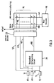
- a semiconductor memory device including a redundant bit line selecting circuit As indicated in Fig. 3, external address signals A0 to Aj are supplied to address buffers 10 to 1j in unit of a single bit.
- the respective address buffers 10 to 1j generate column address signals Y0T to YjT corresponding to the inputted 1-bit address signal.
- a column decoder 120 selects a predetermined bit line BL, so that both of a word line WL selected by a row decoder 110 and a memory cell MC located at a cross point of this bit line are selected.
- a redundant bit line RBL capable of substituting the bit line BL to which a faulty memory cell MC is connected is located within a memory cell array 100.
- the selection signal YR2 becomes an active level
- the column decoder 120 prohibits to select the bit line corresponding to the column address signal entered at this time, and also selects a redundant bit line RBL.
- a redundant bit selecting circuit 30 causes the selection signal YR2 to become active.
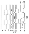
- this redundant bit selecting circuit represented in Fig. 3 owns the following different points. That is, a NAND gate NA1 is employed with having two inputs, namely the sensing signal YRD and the enable signal EN, generated from the ATD signal detecting circuit.
- a precharge signal PCS corresponding to the output from the NAND gate NA1 is supplied to a gate of a P-channel transistor P1 and a gate of an N-channel transistor N1, which are series-connected between the power supply terminal V cc and the ground source GND. Furthermore, a flip-flop 4 is connected to a node YR1 and the sensing signal YRD is supplied to this flip-flop 4.
- the flip-flop 4 is arranged by two sets of NOR gates N01 and N02, and an output of the NOR gate N01 is entered as a first input of the NOR gate N02, whereas an output of the NOR gate N02 is entered as a first input of the NOR gate N01.
- the node YR1 constitutes a second input of the NOR gate N01, and the sensing signal YRD constitutes a second input of the NOR gate N02.
- the flip-flop 4 functions as such a circuit that for a time period during which the sensing signal YRD is at the high level, an inverted potential level of the node YR1 is stored as a selection signal YR2, and the data stored for a time period during which the sensing signal YRD is at the high level is held even when the potential of the node YR1 is changed from the high level into the low level for a time period during which the sensing signal YRD is at the low level.
- Fig. 5 indicates operational waveforms in such a case that the address signals A0 to Aj are changed into A-1, A-2, A-3, and A-2 corresponds to an address of a faulty bit line.
- the enable signal is at a high level during read/write operations. Since the sensing signal YRD is at a low level just before the address signal is changed from A-1 to A-2, the precharge signal PCS is at a high level. Accordingly, the N-channel transistor N1 is brought into the ON state, so that the potential level at the node YR1 becomes the low level and the selection signal YR2 becomes the high level (namely, inactive level).
- the ATD signal detecting circuit 2 causes the low level of the sensing signal YRD to be changed into the high level for a preselected time period.
- the precharge signal PCS becomes the low level during the time period T1.
- the P-channel transistor P1 is brought into the ON state, and the N-channel transistor N1 is brought into the OFF state, so that the charging operation to the node YR1 is carried out.
- the address signal A-2 corresponds to the address of the faulty bit line, no current path is present in all of the selecting circuits 30 to 3j.
- the flip-flop 4 stores therein the data at the low level in response to V cc (high level) of the node YR1, and causes the selection signal YR2 to be brought into the low level (active level).
- the precharge signal PCS becomes a high level after the time period T1 has elapsed. Accordingly, the P-channel transistor P1 is brought into the OFF state, and the N-channel transistor N1 is brought into the ON state, and also the potential at the node YR1 becomes the ground potential. At this time, since the sensing signal YRD is already at the low level, the flip-flop 4 maintains the low level (active level) of the selection signal YR2. It should be noted in this embodiment that the potential at the node YR1 is equal to the ground potential just before the address signal is changed from A-2 to A-3.
- the precharge signal PCS becomes a low level during the time period of T1.
- the P-channel transistor P1 is brought into the ON state and the N-channel transistor N1 is brought into the OFF state.
- the address signal A-3 is not equal to the address of the faulty bit line, at least one of the selecting circuits 30 to 3j forms a current path between the ground source and the node YR1.
- the level of the node YR1 is increased only up to V DC from the ground potential. Since the threshold voltage of the flip-flop 4 is set to be higher than the DC level V DC , the selection signal YR2 becomes the high level (inactive level).
- a semiconductor memory device including a redundant bit line selecting signal generating circuit according to a second embodiment of the present invention will be described.
- a difference point of this second embodiment is such that a clock signal ICLK derived from an internal clock generating circuit 5 is employed instead of the sensing signal YRD supplied to the NAND gate NA1 and the flip-flop 4.
- the internal clock generating circuit 5 is a circuit for generating a clock required to the internal operation in response to an external clock externally supplied.
- the internal clock signal ICLK corresponds to a control clock used to acquire an address, and is furnished to an internal address generating circuit 6. Accordingly, a column address is changed in response to the change in the clock ICLK.
- the clock signal ICLK becomes a high level for a preselected time in synchronism with the change in the address signal.
- This waveform is identical to that of the sensing signal YRD represented in Fig. 5. Since operations of the second embodiment are the same as those of the first embodiment, no explanations thereof are omitted.
Landscapes
- For Increasing The Reliability Of Semiconductor Memories (AREA)
- Static Random-Access Memory (AREA)
Applications Claiming Priority (2)
| Application Number | Priority Date | Filing Date | Title |
|---|---|---|---|
| JP232731/94 | 1994-09-28 | ||
| JP6232731A JP2630274B2 (ja) | 1994-09-28 | 1994-09-28 | 半導体記憶装置 |
Publications (2)
| Publication Number | Publication Date |
|---|---|
| EP0704800A2 true EP0704800A2 (fr) | 1996-04-03 |
| EP0704800A3 EP0704800A3 (fr) | 1999-03-10 |
Family
ID=16943904
Family Applications (1)
| Application Number | Title | Priority Date | Filing Date |
|---|---|---|---|
| EP95115350A Withdrawn EP0704800A3 (fr) | 1994-09-28 | 1995-09-28 | Dispositif de mémoire à semi-conducteur avec circuit de génération d'un signal de sélection d'une ligne de données redondante |
Country Status (3)
| Country | Link |
|---|---|
| EP (1) | EP0704800A3 (fr) |
| JP (1) | JP2630274B2 (fr) |
| KR (1) | KR0172022B1 (fr) |
Families Citing this family (5)
| Publication number | Priority date | Publication date | Assignee | Title |
|---|---|---|---|---|
| JP3401522B2 (ja) | 1998-07-06 | 2003-04-28 | 日本電気株式会社 | ヒューズ回路及び冗長デコーダ回路 |
| JP2000311496A (ja) | 1999-04-28 | 2000-11-07 | Nec Corp | 冗長アドレス設定回路及びこれを内蔵した半導体記憶装置 |
| US8270228B2 (en) | 2009-02-18 | 2012-09-18 | Elpida Memory, Inc. | Semiconductor device having nonvolatile memory element and data processing system including the same |
| JP2010192042A (ja) | 2009-02-18 | 2010-09-02 | Elpida Memory Inc | 半導体装置及びこれを備えるデータ処理システム |
| KR102307044B1 (ko) * | 2021-01-06 | 2021-09-30 | 주식회사 케이에스씨 | 콘크리트 패널의 수직 성형방법 |
Family Cites Families (4)
| Publication number | Priority date | Publication date | Assignee | Title |
|---|---|---|---|---|
| US4546455A (en) * | 1981-12-17 | 1985-10-08 | Tokyo Shibaura Denki Kabushiki Kaisha | Semiconductor device |
| JP2519468B2 (ja) * | 1987-08-26 | 1996-07-31 | 松下電子工業株式会社 | 半導体集積回路 |
| JPH01251397A (ja) * | 1988-03-30 | 1989-10-06 | Toshiba Corp | 半導体メモリ装置 |
| JP2734315B2 (ja) * | 1992-09-24 | 1998-03-30 | 日本電気株式会社 | 半導体メモリ装置 |
-
1994
- 1994-09-28 JP JP6232731A patent/JP2630274B2/ja not_active Expired - Fee Related
-
1995
- 1995-09-28 EP EP95115350A patent/EP0704800A3/fr not_active Withdrawn
- 1995-09-28 KR KR1019950032319A patent/KR0172022B1/ko not_active Expired - Fee Related
Non-Patent Citations (1)
| Title |
|---|
| None |
Also Published As
| Publication number | Publication date |
|---|---|
| KR0172022B1 (ko) | 1999-03-30 |
| JP2630274B2 (ja) | 1997-07-16 |
| EP0704800A3 (fr) | 1999-03-10 |
| KR960012035A (ko) | 1996-04-20 |
| JPH0896594A (ja) | 1996-04-12 |
Similar Documents
| Publication | Publication Date | Title |
|---|---|---|
| US5657280A (en) | Defective cell repairing circuit and method of semiconductor memory device | |
| US4532607A (en) | Programmable circuit including a latch to store a fuse's state | |
| US5140554A (en) | Integrated circuit fuse-link tester and test method | |
| US6791897B2 (en) | Word line driving circuit | |
| US5485424A (en) | Semiconductor memory and redundant-address writing method | |
| US5414659A (en) | Semiconductor memory device having address transition detector quickly enabling redundancy decoder | |
| JPH0652685A (ja) | パワーオンリセット制御型ラッチ型行ラインリピータを有する半導体メモリ | |
| JPH0334640B2 (fr) | ||
| JPH08339699A (ja) | 行デコーダおよびdram | |
| JPS63220500A (ja) | 半導体記憶装置の冗長回路 | |
| US4975881A (en) | Semiconductor memory device provided with an improved redundant decoder | |
| US5333122A (en) | Electrically erasable and programmable non-volatile semiconductor memory device having word line voltage control circuit using internal voltage booster circuit | |
| GB2296986A (en) | A semiconductor memory including voltage boosting generators | |
| US20020067633A1 (en) | Semiconductor integrated circuit | |
| JPH08339696A (ja) | Ramアレイをテストする方法 | |
| EP0881571B1 (fr) | Dispositif de mémoire à semiconducteur avec rédondance | |
| EP0121394A2 (fr) | Dispositif de mémoire à semi-conducteur incorporant des cellules de mémoire redondantes | |
| US7436729B2 (en) | Fuse circuit and semiconductor device using fuse circuit thereof | |
| EP0740308B1 (fr) | Dispositif de mémoire dynamique à semi-conducteur | |
| JP3015652B2 (ja) | 半導体メモリ装置 | |
| JP2760326B2 (ja) | 半導体記憶装置 | |
| US5892776A (en) | Semiconductor memory and test method incorporating selectable clock signal modes | |
| US20050007843A1 (en) | Redundancy circuit in semiconductor memory device having a multiblock structure | |
| JP3841252B2 (ja) | ツルー/コンプリメント冗長構造を有する半導体メモリ装置 | |
| EP0704800A2 (fr) | Dispositif de mémoire à semi-conducteur avec circuit de génération d'un signal de sélection d'une ligne de données redondante |
Legal Events
| Date | Code | Title | Description |
|---|---|---|---|
| PUAI | Public reference made under article 153(3) epc to a published international application that has entered the european phase |
Free format text: ORIGINAL CODE: 0009012 |
|
| AK | Designated contracting states |
Kind code of ref document: A2 Designated state(s): DE FR GB |
|
| PUAL | Search report despatched |
Free format text: ORIGINAL CODE: 0009013 |
|
| AK | Designated contracting states |
Kind code of ref document: A3 Designated state(s): DE FR GB |
|
| 17P | Request for examination filed |
Effective date: 19990319 |
|
| 17Q | First examination report despatched |
Effective date: 20010629 |
|
| STAA | Information on the status of an ep patent application or granted ep patent |
Free format text: STATUS: THE APPLICATION HAS BEEN WITHDRAWN |
|
| 18W | Application withdrawn |
Withdrawal date: 20020109 |