EP0704890A2 - Méthode d'évaluation d'un dispositif semi-conducteur MIS - Google Patents
Méthode d'évaluation d'un dispositif semi-conducteur MIS Download PDFInfo
- Publication number
- EP0704890A2 EP0704890A2 EP95115467A EP95115467A EP0704890A2 EP 0704890 A2 EP0704890 A2 EP 0704890A2 EP 95115467 A EP95115467 A EP 95115467A EP 95115467 A EP95115467 A EP 95115467A EP 0704890 A2 EP0704890 A2 EP 0704890A2
- Authority
- EP
- European Patent Office
- Prior art keywords
- treatment
- mis
- insulative layer
- voltage
- semiconductor device
- Prior art date
- Legal status (The legal status is an assumption and is not a legal conclusion. Google has not performed a legal analysis and makes no representation as to the accuracy of the status listed.)
- Withdrawn
Links
Images
Classifications
-
- G—PHYSICS
- G01—MEASURING; TESTING
- G01R—MEASURING ELECTRIC VARIABLES; MEASURING MAGNETIC VARIABLES
- G01R31/00—Arrangements for testing electric properties; Arrangements for locating electric faults; Arrangements for electrical testing characterised by what is being tested not provided for elsewhere
- G01R31/28—Testing of electronic circuits, e.g. by signal tracer
- G01R31/282—Testing of electronic circuits specially adapted for particular applications not provided for elsewhere
- G01R31/2831—Testing of materials or semi-finished products, e.g. semiconductor wafers or substrates
-
- G—PHYSICS
- G01—MEASURING; TESTING
- G01R—MEASURING ELECTRIC VARIABLES; MEASURING MAGNETIC VARIABLES
- G01R31/00—Arrangements for testing electric properties; Arrangements for locating electric faults; Arrangements for electrical testing characterised by what is being tested not provided for elsewhere
- G01R31/26—Testing of individual semiconductor devices
- G01R31/2648—Characterising semiconductor materials
-
- H—ELECTRICITY
- H10—SEMICONDUCTOR DEVICES; ELECTRIC SOLID-STATE DEVICES NOT OTHERWISE PROVIDED FOR
- H10P—GENERIC PROCESSES OR APPARATUS FOR THE MANUFACTURE OR TREATMENT OF DEVICES COVERED BY CLASS H10
- H10P74/00—Testing or measuring during manufacture or treatment of wafers, substrates or devices
- H10P74/20—Testing or measuring during manufacture or treatment of wafers, substrates or devices characterised by the properties tested or measured, e.g. structural or electrical properties
- H10P74/207—Electrical properties, e.g. testing or measuring of resistance, deep levels or capacitance-voltage characteristics
Definitions
- This invention relates in general to a method of evaluating a MIS-type semiconductor device which comprises an insulative layer and a conductive layer formed one after another on a semiconductor substrate, and more particularly to a method of measuring the carrier trap density in the insulative layer in a MIS-type semiconductor device.
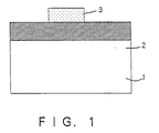
- FIG. 1 shows the structure of a MIS-type semiconductor device used for this kind of measurement.
- 1 is a semiconductor substrate, for example, made of N-type silicon
- 2 is an insulative layer such as a silicon oxide layer
- 3 is a conductive layer such as an aluminum or polysilicon layer.
- Step-wise bias voltage is applied between the conductive layer 3 and the semiconductor substrate 1 of such a MIS-type semiconductor device and the capacitance is measured to obtain the C-V characteristic curve.
- a high frequency signal voltage is added to obtain the high frequency C-V characteristic curve and a low frequency signal voltage is added to obtain the quasi-static C-V characteristic curve.
- each C-V characteristic curve can be obtained theoretically, the actual curve deviates from the theoretical curve because there are four types of electric charges as mentioned above.
- the amounts of charges due to the fixed oxide charges and the interface trapped charges are obtained based on the amount of this deviation.
- the amount of mobile ionic charges can also be calculated by using the TVS method (for example, refer to J. Electrochem. Soc.,; Solid State Science, Vol. 118, No. 4, Apl., 1971, pp 601-608).
- the method described below uses the BT (Bias Temperature) treatment and obtains this amount based on the shift of the C-V characteristics from before to after the BT treatment (for example, refer to Japanese Journal of Applied Physics, Vol. 6, No. 2, Feb., 1967, pp 191-204).
- the mobile ionic charges in the insulative layer are alkali metal (Li, Na, K, etc.) ions and they have positive charges. Since the mobile ionic charges can easily move in the insulative layer when they are heated to 100°C or higher, the amount of the mobile ionic charges can be determined by making them move in the insulative layer by conducting the BT treatment where a prescribed positive or negative voltage is applied on the conductive layer at a prescribed temperature for a prescribed duration of time.
- This method which uses the BT treatment is generally a method to study the electrical instability of the insulative layer of a MIS-type semiconductor device.
- a positive BT treatment results in movement of the mobile ionic charges in the insulative layer toward the semiconductor substrate and an increase in the amount of positive electric charges in the insulative layer near the semiconductor substrate.
- the electrons in the semiconductor substrate are attracted toward the surface of the semiconductor substrate, and, due to the influence of the temperature and the electric field, some electrons are captured in electron traps in the insulative layer. Captured electrons in the electron traps increase the amount of negative electric charges in the insulative layer near the semiconductor substrate.
- a negative BT treatment results in movement of the mobile ionic charges in the insulative layer toward the conductive layer and a decrease in the amount of positive electric charges in the insulative layer near the semiconductor substrate.
- the holes in the semiconductor substrate are attracted toward the surface of the semiconductor substrate, and, due to the influence of the temperature and the electric field, some holes are captured in hole traps in the insulative layer. Because of this, there is a problem in that when the amount of mobile ionic charges in the insulative layer is large, the C-V characteristic curve after the negative BT treatment shifts toward the positive voltage along the voltage axis, making it impossible to quantitatively measure the amount of the hole traps.
- the object of the present invention is to provide a method of evaluating the electrical instability of the insulative layer with high reproducibility and accuracy when evaluating the electrical characteristics of a MIS-type semiconductor device.
- the present invention attempts to solve the problem described above by introducing a method of evaluating a MIS -type semiconductor device which comprises an insulative layer (s) and a conductive layer(s) formed one after another on a semiconductor substrate wherein: using a sample with an interface trapped charge density of 1 ⁇ 10 10 /cm 2 ⁇ eV or less and a mobile ionic charge density of 3 ⁇ 1010 /cm2 or less in said insulative layer, said MIS- type semiconductor device is treated by applying a positive or negative voltage in the range of 1-5 MV/cm between said semiconductor substrate and said conductive layer at a temperature of 100-300°C and maintaining this voltage for 1-60 minutes (hereafter referred to as "BT treatment"); before and after said BT treatment, the capacitance-voltage characteristics (hereafter referred to as "C-V characteristics) of said MIS -type semiconductor device are measured at room temperature; and the carrier trap density of said insulative layer is determined based on the shift of the flat band voltage of said C
- the present invention makes it possible to take accurate relative measurements of the amount of the carrier traps in the insulative layer in a MIS-type semiconductor device by reducing the amount of the mobile ionic charges and the interface trapped charge in the insulative layer in the MIS -type semiconductor device and limiting the conditions of the BT treatment.
- Figure 1 is a schematic cross-section showing the configuration of a MIS-type semiconductor device.
- a silicon wafer(s) grown by using the CZ method was prepared which had a diameter of 5 inches, a plane orientation of (100), a conductivity type of P-type, a specific resistance of 10 ohm-cm, and an interstitial oxygen concentration of approximately 1.4 ⁇ 1018 atoms/cm3.
- a MIS capacitor was then prepared according to the following conditions.
- a Si wafer(s) went through a cleaning process to clean its surface before the oxidation process. After drying up, it was immediately inserted into an oxidation furnace.
- a gate oxide layer was grown to 50 nm in a dry oxygen ambient at 1000°C for 60 minutes.
- the samples oxidized here were designated as No. 1-1 to 1-3.
- Some samples which went through cleaning and oxidization under the same conditions additionally received a heat treatment in a nitrogen ambient (hereafter referred to as "nitrogen annealing") for an hour and were designated as No. 2-1 to 2-3.
- the silicon wafers and MIS capacitors described above were prepared in a very high cleanliness where the atmosphere in the clean room, the dew point of the gas(es), the grade of the cleaning solution(s), manufacturing apparatus, perspiration and clothing of the operators, etc. were sufficiently controlled.
- a BT treatment (temperature: 250°C, electric field intensity: 3 MV/cm, time: 30 minutes) was conducted, and the C-V characteristic curve was measured at room temperature before and after this BT treatment.
- the amount of charges calculated from the shift of V FB is shown in Table 1.
- the C-V characteristic curves for the samples No. 2-1 to 2-3 simply shifted along the voltage axis and its slope was not distorted. This indicates that new interface trapped charges were not generated by the BT treatment.
- the interface state density at a mid-gap voltage obtained from the quasi-static C-V characteristics was measured at 6 points per wafer. It was 3.9 ⁇ 10 9 to 8.3 ⁇ 10 9 /cm 2 ⁇ eV for the samples No. 1-1 to 1-3, and 2.2 ⁇ 10 9 /cm 2 ⁇ eV or less for the samples No. 2-1 to 2-3.
- Table 1 indicates that while the amount of the mobile ionic charges is 3 ⁇ 1010 /cm2 or less and the hole trap density is approximately 7 x 10¹⁰ /cm2 in the insulative layer which received the nitrogen annealing treatment after the formation of oxide layer, the electron trap density is approximately 1.2 ⁇ 1010 to 4.6 ⁇ 1010 /cm2 and the hole trap density is approximately 4 ⁇ 1011 /cm2 in the insulative layer which did not receive the nitrogen annealing treatment.
- a positive value indicates that positive electric charges, i.e. the charge due to the holes captured by hole traps, was generated in the insulative layer near the semiconductor substrate by the BT treatment (after the BT treatment, the C-V characteristic curve shifts in the direction of the negative voltage along the voltage axis), and a negative value indicates that negative electric charge, i.e. the charge due to the electrons captured by electron traps, was generated in the insulative layer near the semiconductor substrate by the BT treatment (after the BT treatment, the C-V characteristic curve shifts in the positive direction along the voltage axis).
- a silicon wafer(s) grown by using the CZ method was prepared which had a diameter of 5 inches, a plane orientation of (100), a conductivity type of P-type, a specific resistance of 10 ohm-cm, and an interstitial oxygen concentration of approximately 1.4 ⁇ 1018 atoms/cm3.
- a MIS capacitor was then prepared according to the following conditions.
- a Si wafer(s) went through a cleaning process to clean its surface before the oxidation process. After drying up, it was immediately inserted into an oxidation furnace.
- a gate oxide layer was grown to 50 mn in a wet oxygen atmosphere at 950°C for 8.5 minutes, after which one hour of nitrogen annealing was added.
- the dew point of hydrogen was controlled, and the samples with a hydrogen dew point of -62°C were designated as No. 3-1 to 3-3, the samples with a hydrogen dew point of -68°C were designated as No. 4 -1 to 4-3, and the samples with a hydrogen dew point of -74 °C were designated as No. 5-1 to 5-3.
- the vacuum evaporation method was employed to form an approximately 1 micrometer-thick Al electrode(s) using a metal mask(s) on the silicon oxide layer(s). After removing the silicon oxide layer(s) on the back side, a heat treatment was conducted at 400°C for 30 minutes in a mixed atmosphere of 3% hydrogen and 97% nitrogen.
- a BT treatment (temperature: 250°C, electric field intensity: 3 MV/cm, time: 30 minutes) was conducted, and the C-V characteristic curve was measured at room temperature before and after this BT treatment.
- the amount of charges calculated from the shift of V BF is shown in Table 2.
- the C-V characteristic curves not only shifted along the voltage axis but also its slope was distorted. This indicates that new interface trapped charges were generated by the BT treatment.
- Table 2 indicates that because of the reduced purity due to an increase in the dew point of the ambient gas in the oxide layer forming process, there are mobile ionic charges on the order of 1011-1012 /cm2 in the insulative layer and hence it is not possible to determine the density of electron traps or hole traps.
- a positive value indicates that the BT treatment increased the amount of the mobile ionic charges in the insulative layer near the semiconductor substrate (after the BT treatment, the C-V characteristic curve shifts in the negative direction along the voltage axis), and a negative value indicates that the BT treatment decreased the amount of the mobile ionic charges in the insulative layer near the semiconductor substrate (after the BT treatment, the C-V characteristic curve shifts in the positive direction along the voltage axis).
- Table 2 Sample Wafer No.
- the present invention makes it possible to measure carrier traps, which have been impossible to measure with conventional methods, by using a method of evaluating a MIS-type semiconductor device wherein: using a sample with an interface trapped charge density of 1 ⁇ 10 10 /cm 2 ⁇ eV or less and a mobile ionic charge density of 3 ⁇ 1010/cm2 or less in said insulative layer, said MIS-type semiconductor device is given a BT treatment by applying a positive or negative voltage in the range of 1-5 MV/cm between said semiconductor substrate and said conductive layer at a temperature of 100 -300°C and maintaining this voltage for 1-60 minutes; before and after said BT treatment, the C-V characteristics of said MIS-type semiconductor device are measured at room temperature; and the carrier trap density of said insulative layer is determined based on the shift of the flat band voltage of said C-V characteristics from before to after said BT treatment.
Landscapes
- Engineering & Computer Science (AREA)
- General Engineering & Computer Science (AREA)
- Physics & Mathematics (AREA)
- General Physics & Mathematics (AREA)
- Testing Or Measuring Of Semiconductors Or The Like (AREA)
- Insulated Gate Type Field-Effect Transistor (AREA)
Applications Claiming Priority (2)
| Application Number | Priority Date | Filing Date | Title |
|---|---|---|---|
| JP261094/94 | 1994-09-30 | ||
| JP6261094A JPH08102481A (ja) | 1994-09-30 | 1994-09-30 | Mis型半導体装置の評価方法 |
Publications (2)
| Publication Number | Publication Date |
|---|---|
| EP0704890A2 true EP0704890A2 (fr) | 1996-04-03 |
| EP0704890A3 EP0704890A3 (fr) | 1997-05-02 |
Family
ID=17357007
Family Applications (1)
| Application Number | Title | Priority Date | Filing Date |
|---|---|---|---|
| EP95115467A Withdrawn EP0704890A3 (fr) | 1994-09-30 | 1995-09-29 | Méthode d'évaluation d'un dispositif semi-conducteur MIS |
Country Status (3)
| Country | Link |
|---|---|
| US (1) | US5701088A (fr) |
| EP (1) | EP0704890A3 (fr) |
| JP (1) | JPH08102481A (fr) |
Cited By (2)
| Publication number | Priority date | Publication date | Assignee | Title |
|---|---|---|---|---|
| US6362097B1 (en) * | 1998-07-14 | 2002-03-26 | Applied Komatsu Technlology, Inc. | Collimated sputtering of semiconductor and other films |
| CN111785656A (zh) * | 2020-07-28 | 2020-10-16 | 哈尔滨工业大学 | 电子器件氧化层中固定负电荷陷阱的检测方法 |
Families Citing this family (7)
| Publication number | Priority date | Publication date | Assignee | Title |
|---|---|---|---|---|
| JPH08130214A (ja) * | 1994-09-07 | 1996-05-21 | Seiko Instr Inc | 半導体装置およびその製造方法 |
| US6136669A (en) * | 1998-07-21 | 2000-10-24 | International Business Machines Corporation | Mobile charge immune process |
| JP2001077648A (ja) * | 1999-09-06 | 2001-03-23 | Sony Corp | ポリフェイズフィルタおよびこれを使用した受信機 |
| JP3736740B2 (ja) * | 2000-12-12 | 2006-01-18 | シャープ株式会社 | 絶縁膜容量評価装置および絶縁膜容量評価方法 |
| JP2009239201A (ja) * | 2008-03-28 | 2009-10-15 | Sanyo Electric Co Ltd | ゲート絶縁膜の評価方法 |
| JP6119680B2 (ja) * | 2014-06-25 | 2017-04-26 | 信越半導体株式会社 | 半導体基板の欠陥領域の評価方法 |
| JP6239681B2 (ja) * | 2016-05-02 | 2017-11-29 | ローム株式会社 | 半導体装置 |
Family Cites Families (6)
| Publication number | Priority date | Publication date | Assignee | Title |
|---|---|---|---|---|
| JPS5565145A (en) * | 1978-11-11 | 1980-05-16 | Agency Of Ind Science & Technol | Characteristic measuring method for charge trap center in insulator |
| JPS5775439A (en) * | 1980-10-30 | 1982-05-12 | Oki Electric Ind Co Ltd | Judgement of stability of semiconductor device |
| JPS61159748A (ja) * | 1985-01-08 | 1986-07-19 | Oki Electric Ind Co Ltd | トラツプ分布測定方法 |
| JPS6312144A (ja) * | 1986-07-03 | 1988-01-19 | Oki Electric Ind Co Ltd | 半導体素子の評価方法 |
| US4978915A (en) * | 1989-11-07 | 1990-12-18 | At&T Bell Laboratories | Method of manufacturing semiconductor devices involving the detection of impurities |
| JPH04134842A (ja) * | 1990-09-27 | 1992-05-08 | Toshiba Corp | 絶縁膜の信頼性評価方法及び装置 |
-
1994
- 1994-09-30 JP JP6261094A patent/JPH08102481A/ja active Pending
-
1995
- 1995-09-27 US US08/534,460 patent/US5701088A/en not_active Expired - Fee Related
- 1995-09-29 EP EP95115467A patent/EP0704890A3/fr not_active Withdrawn
Cited By (3)
| Publication number | Priority date | Publication date | Assignee | Title |
|---|---|---|---|---|
| US6362097B1 (en) * | 1998-07-14 | 2002-03-26 | Applied Komatsu Technlology, Inc. | Collimated sputtering of semiconductor and other films |
| CN111785656A (zh) * | 2020-07-28 | 2020-10-16 | 哈尔滨工业大学 | 电子器件氧化层中固定负电荷陷阱的检测方法 |
| CN111785656B (zh) * | 2020-07-28 | 2023-08-15 | 哈尔滨工业大学 | 电子器件氧化层中固定负电荷陷阱的检测方法 |
Also Published As
| Publication number | Publication date |
|---|---|
| US5701088A (en) | 1997-12-23 |
| EP0704890A3 (fr) | 1997-05-02 |
| JPH08102481A (ja) | 1996-04-16 |
Similar Documents
| Publication | Publication Date | Title |
|---|---|---|
| KR100475040B1 (ko) | 실리콘카바이드상의산화막결함저감방법 | |
| US3793090A (en) | Method for stabilizing fet devices having silicon gates and composite nitride-oxide gate dielectrics | |
| Nishioka et al. | Dielectric Characteristics of Double Layer Structure of Extremely Thin Ta2 O 5/SiO2 on Si | |
| Nemirovsky et al. | The interface between Hg1− xCdxTe and its native oxide | |
| Liu et al. | Characterization of charge trapping and high-field endurance for 15-nm thermally nitrided oxides | |
| EP0704890A2 (fr) | Méthode d'évaluation d'un dispositif semi-conducteur MIS | |
| Shiono et al. | Surface State Formation during Long-Term Bias-Temperature Stress Aging of Thin SiO2–Si Interfaces | |
| Dickey et al. | Improved dielectric properties for anodic aluminum oxide films by soft/hard two‐step electrolytic anodization | |
| US5736454A (en) | Method for making a silicon dioxide layer on a silicon substrate by pure water anodization followed by rapid thermal densification | |
| Osburn et al. | Improved dielectric reliability of SiO2 films with polycrystalline silicon electrodes | |
| Das et al. | Effect of epilayer characteristics and processing conditions on the thermally oxidized SiO2/SiC interface | |
| Fogels et al. | Characterization of Surface States at the Si‐SiO2 Interface Using the Quasi‐Static Technique | |
| US5470611A (en) | Method for forming an oxide film of a semiconductor | |
| Streever et al. | Surface states at the n GaAs SiO2 interface from conductance and capacitance measurements | |
| Hillen et al. | The influence of mobile ions on the Si/SiO2 interface traps | |
| Wang et al. | Relationships of the Chemical and Electrical Interfacial Properties of Germanium‐SiO2 Systems | |
| EP0608745A2 (fr) | Procédé de fabrication de composants MOS | |
| Hsieh et al. | Study and improvement of anomalous interface states of metal‐oxide‐semiconductor structures induced by rapid thermal post‐oxide annealing | |
| Andersson et al. | Surface-potential dependence of interface-state passivation in metal–tunnel-oxide–silicon diodes | |
| Haberle et al. | MOS device fabrication using sputter-deposited gate oxide and polycrystalline silicon layers | |
| JPH11297704A (ja) | 酸素析出物密度の評価方法 | |
| JP4305800B2 (ja) | シリコンウエハ表面の窒化物評価方法 | |
| Jelenkovic et al. | Effect of implanted fluorine on MOS structures with sputtered SiO2 insulator | |
| Tay et al. | Thin gate and poly oxides by high pressure silicon oxidation | |
| Zetterling et al. | Comparison of thermal gate oxides on silicon and carbon face p-type 6H silicon carbide |
Legal Events
| Date | Code | Title | Description |
|---|---|---|---|
| PUAI | Public reference made under article 153(3) epc to a published international application that has entered the european phase |
Free format text: ORIGINAL CODE: 0009012 |
|
| AK | Designated contracting states |
Kind code of ref document: A2 Designated state(s): DE FR GB |
|
| RTI1 | Title (correction) | ||
| PUAL | Search report despatched |
Free format text: ORIGINAL CODE: 0009013 |
|
| AK | Designated contracting states |
Kind code of ref document: A3 Designated state(s): DE FR GB |
|
| 17P | Request for examination filed |
Effective date: 19970709 |
|
| 17Q | First examination report despatched |
Effective date: 19990614 |
|
| STAA | Information on the status of an ep patent application or granted ep patent |
Free format text: STATUS: THE APPLICATION IS DEEMED TO BE WITHDRAWN |
|
| 18D | Application deemed to be withdrawn |
Effective date: 19991026 |