EP0704893A2 - Procédé de planarisation amélioré - Google Patents
Procédé de planarisation amélioré Download PDFInfo
- Publication number
- EP0704893A2 EP0704893A2 EP95114889A EP95114889A EP0704893A2 EP 0704893 A2 EP0704893 A2 EP 0704893A2 EP 95114889 A EP95114889 A EP 95114889A EP 95114889 A EP95114889 A EP 95114889A EP 0704893 A2 EP0704893 A2 EP 0704893A2
- Authority
- EP
- European Patent Office
- Prior art keywords
- conductor
- conducting
- reticulated
- layer
- ild
- Prior art date
- Legal status (The legal status is an assumption and is not a legal conclusion. Google has not performed a legal analysis and makes no representation as to the accuracy of the status listed.)
- Withdrawn
Links
Images

Classifications
-
- H—ELECTRICITY
- H10—SEMICONDUCTOR DEVICES; ELECTRIC SOLID-STATE DEVICES NOT OTHERWISE PROVIDED FOR
- H10W—GENERIC PACKAGES, INTERCONNECTIONS, CONNECTORS OR OTHER CONSTRUCTIONAL DETAILS OF DEVICES COVERED BY CLASS H10
- H10W20/00—Interconnections in chips, wafers or substrates
- H10W20/40—Interconnections external to wafers or substrates, e.g. back-end-of-line [BEOL] metallisations or vias connecting to gate electrodes
- H10W20/41—Interconnections external to wafers or substrates, e.g. back-end-of-line [BEOL] metallisations or vias connecting to gate electrodes characterised by their conductive parts
- H10W20/43—Layouts of interconnections
-
- H—ELECTRICITY
- H10—SEMICONDUCTOR DEVICES; ELECTRIC SOLID-STATE DEVICES NOT OTHERWISE PROVIDED FOR
- H10P—GENERIC PROCESSES OR APPARATUS FOR THE MANUFACTURE OR TREATMENT OF DEVICES COVERED BY CLASS H10
- H10P95/00—Generic processes or apparatus for manufacture or treatments not covered by the other groups of this subclass
- H10P95/06—Planarisation of inorganic insulating materials
- H10P95/062—Planarisation of inorganic insulating materials involving a dielectric removal step
-
- H—ELECTRICITY
- H10—SEMICONDUCTOR DEVICES; ELECTRIC SOLID-STATE DEVICES NOT OTHERWISE PROVIDED FOR
- H10W—GENERIC PACKAGES, INTERCONNECTIONS, CONNECTORS OR OTHER CONSTRUCTIONAL DETAILS OF DEVICES COVERED BY CLASS H10
- H10W20/00—Interconnections in chips, wafers or substrates
- H10W20/01—Manufacture or treatment
- H10W20/031—Manufacture or treatment of conductive parts of the interconnections
-
- H—ELECTRICITY
- H10—SEMICONDUCTOR DEVICES; ELECTRIC SOLID-STATE DEVICES NOT OTHERWISE PROVIDED FOR
- H10W—GENERIC PACKAGES, INTERCONNECTIONS, CONNECTORS OR OTHER CONSTRUCTIONAL DETAILS OF DEVICES COVERED BY CLASS H10
- H10W20/00—Interconnections in chips, wafers or substrates
- H10W20/01—Manufacture or treatment
- H10W20/071—Manufacture or treatment of dielectric parts thereof
- H10W20/092—Manufacture or treatment of dielectric parts thereof by smoothing the dielectric parts
Definitions
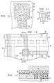
- Figure 5 shows a reticulated conductor 52 and a minimum width conductor 24 formed on a substrate 20.
- Reticulated conductor 52 has an interior region 50 where conducting material has been removed.
- Such a conductor may be designed directly into the mask pattern, such that interior region 50 is created at the same time as the outer walls of the conductor.
- Conductor 52 can be described as comprising a set of connected conducting segments: right segment 44, left segment 46, bottom segment 48, and top segment 49. Segments 44 and 46 provide multiple current paths between top and bottom segments 49 and 48.
- Figure 6 contains a cross-sectional elevation of Figure 5, taken through small conductor 24 and left and right segments 46 and 44 along section line 6-6.
- a seed layer 30 and HDP oxide layer 32 deposition are shown to illustrate the excellent ILD planarity achievable above the conductor segments 44 and 46, as well as conductor 24, where widths of such are all smaller than the critical width.
Landscapes
- Internal Circuitry In Semiconductor Integrated Circuit Devices (AREA)
- Mechanical Treatment Of Semiconductor (AREA)
Applications Claiming Priority (2)
| Application Number | Priority Date | Filing Date | Title |
|---|---|---|---|
| US08/315,529 US5686356A (en) | 1994-09-30 | 1994-09-30 | Conductor reticulation for improved device planarity |
| US315529 | 1994-09-30 |
Publications (2)
| Publication Number | Publication Date |
|---|---|
| EP0704893A2 true EP0704893A2 (fr) | 1996-04-03 |
| EP0704893A3 EP0704893A3 (fr) | 1997-05-02 |
Family
ID=23224846
Family Applications (1)
| Application Number | Title | Priority Date | Filing Date |
|---|---|---|---|
| EP95114889A Withdrawn EP0704893A3 (fr) | 1994-09-30 | 1995-09-21 | Procédé de planarisation amélioré |
Country Status (3)
| Country | Link |
|---|---|
| US (3) | US5686356A (fr) |
| EP (1) | EP0704893A3 (fr) |
| JP (1) | JPH08195395A (fr) |
Cited By (4)
| Publication number | Priority date | Publication date | Assignee | Title |
|---|---|---|---|---|
| EP0841695A3 (fr) * | 1996-11-08 | 1998-05-20 | W.L. GORE & ASSOCIATES, INC. | Base très plane à CDT faible et méthode de fabrication associée |
| WO1999047728A1 (fr) * | 1998-03-20 | 1999-09-23 | Applied Materials, Inc. | Procede et dispositif de depot et d'attaque chimique d'une couche dielectrique |
| WO2002089200A3 (fr) * | 2001-05-01 | 2003-01-23 | Koninkl Philips Electronics Nv | Procede de fabrication d'un dispositif semi-conducteur |
| CN107611261A (zh) * | 2017-08-14 | 2018-01-19 | 信利半导体有限公司 | 一种柔性oled基板的制作方法 |
Families Citing this family (43)
| Publication number | Priority date | Publication date | Assignee | Title |
|---|---|---|---|---|
| US5345394A (en) | 1992-02-10 | 1994-09-06 | S-Mos Systems, Inc. | Method for generating power slits |
| US5686356A (en) | 1994-09-30 | 1997-11-11 | Texas Instruments Incorporated | Conductor reticulation for improved device planarity |
| JP2930025B2 (ja) * | 1996-08-29 | 1999-08-03 | 日本電気株式会社 | 半導体装置及びその製造方法 |
| US6184158B1 (en) * | 1996-12-23 | 2001-02-06 | Lam Research Corporation | Inductively coupled plasma CVD |
| US6171896B1 (en) * | 1997-02-03 | 2001-01-09 | Taiwan Semiconductor Manufacturing Company | Method of forming shallow trench isolation by HDPCVD oxide |
| EP0887847A1 (fr) * | 1997-04-15 | 1998-12-30 | STMicroelectronics S.r.l. | Procédé de passivation finale de circuits intégrés |
| US5885894A (en) * | 1997-06-25 | 1999-03-23 | United Microelectronics Corporation | Method of planarizing an inter-layer dielectric layer |
| US6054376A (en) * | 1997-12-31 | 2000-04-25 | Intel Corporation | Method of sealing a semiconductor substrate |
| US6162586A (en) * | 1998-05-06 | 2000-12-19 | Philips Electronics North America Corp. | Method for substantially preventing footings in chemically amplified deep ultra violet photoresist layers |
| US6103457A (en) * | 1998-05-28 | 2000-08-15 | Philips Electronics North America Corp. | Method for reducing faceting on a photoresist layer during an etch process |
| US6218251B1 (en) | 1998-11-06 | 2001-04-17 | Advanced Micro Devices, Inc. | Asymmetrical IGFET devices with spacers formed by HDP techniques |
| US6133151A (en) * | 1999-05-10 | 2000-10-17 | Worldwide Semiconductor Manufacturing Corp. | HDP-CVD method for spacer formation |
| US6043152A (en) * | 1999-05-14 | 2000-03-28 | Taiwan Semiconductor Manufacturing Company | Method to reduce metal damage in the HDP-CVD process by using a sacrificial dielectric film |
| US6319796B1 (en) | 1999-08-18 | 2001-11-20 | Vlsi Technology, Inc. | Manufacture of an integrated circuit isolation structure |
| US6261957B1 (en) | 1999-08-20 | 2001-07-17 | Taiwan Semiconductor Manufacturing Company | Self-planarized gap-filling by HDPCVD for shallow trench isolation |
| JP4587604B2 (ja) | 2001-06-13 | 2010-11-24 | 富士通セミコンダクター株式会社 | 半導体装置の製造方法 |
| US6709977B2 (en) * | 2002-02-12 | 2004-03-23 | Broadcom Corporation | Integrated circuit having oversized components and method of manafacture thereof |
| US7077992B2 (en) | 2002-07-11 | 2006-07-18 | Molecular Imprints, Inc. | Step and repeat imprint lithography processes |
| US6932934B2 (en) | 2002-07-11 | 2005-08-23 | Molecular Imprints, Inc. | Formation of discontinuous films during an imprint lithography process |
| US8349241B2 (en) | 2002-10-04 | 2013-01-08 | Molecular Imprints, Inc. | Method to arrange features on a substrate to replicate features having minimal dimensional variability |
| JP4387654B2 (ja) * | 2002-10-10 | 2009-12-16 | パナソニック株式会社 | 半導体装置およびその製造方法 |
| US7089522B2 (en) * | 2003-06-11 | 2006-08-08 | Chartered Semiconductor Manufacturing, Ltd. | Device, design and method for a slot in a conductive area |
| US7012021B2 (en) * | 2004-01-29 | 2006-03-14 | Taiwan Semiconductor Mfg | Method for end point detection polysilicon chemical mechanical polishing in an anti-fuse memory device |
| DE102004019588A1 (de) * | 2004-04-22 | 2005-11-17 | Osram Opto Semiconductors Gmbh | Verfahren zur Strukturierung von zumindest einer Schicht sowie elektrisches Bauelement mit Strukturen aus der Schicht |
| US20050245069A1 (en) * | 2004-04-28 | 2005-11-03 | Contour Semiconductor, Inc. | Substrate flattening method |
| US20050253307A1 (en) * | 2004-05-11 | 2005-11-17 | Molecualr Imprints, Inc. | Method of patterning a conductive layer on a substrate |
| DE102004029519A1 (de) * | 2004-06-18 | 2006-01-12 | Infineon Technologies Ag | Verfahren zum Herstellen einer Schicht-Anordnung |
| US7355283B2 (en) * | 2005-04-14 | 2008-04-08 | Sandisk Corporation | Rigid wave pattern design on chip carrier substrate and printed circuit board for semiconductor and electronic sub-system packaging |
| KR100643853B1 (ko) * | 2005-06-04 | 2006-11-14 | 삼성전자주식회사 | 반도체 소자의 다마신 배선 형성 방법 및 이에 의해 제조된반도체 소자 |
| US7906058B2 (en) | 2005-12-01 | 2011-03-15 | Molecular Imprints, Inc. | Bifurcated contact printing technique |
| US7803308B2 (en) | 2005-12-01 | 2010-09-28 | Molecular Imprints, Inc. | Technique for separating a mold from solidified imprinting material |
| US7670530B2 (en) | 2006-01-20 | 2010-03-02 | Molecular Imprints, Inc. | Patterning substrates employing multiple chucks |
| MY144847A (en) | 2005-12-08 | 2011-11-30 | Molecular Imprints Inc | Method and system for double-sided patterning of substrates |
| US8850980B2 (en) | 2006-04-03 | 2014-10-07 | Canon Nanotechnologies, Inc. | Tessellated patterns in imprint lithography |
| US7802978B2 (en) | 2006-04-03 | 2010-09-28 | Molecular Imprints, Inc. | Imprinting of partial fields at the edge of the wafer |
| US7780893B2 (en) | 2006-04-03 | 2010-08-24 | Molecular Imprints, Inc. | Method of concurrently patterning a substrate having a plurality of fields and a plurality of alignment marks |
| US8142850B2 (en) | 2006-04-03 | 2012-03-27 | Molecular Imprints, Inc. | Patterning a plurality of fields on a substrate to compensate for differing evaporation times |
| US8012395B2 (en) | 2006-04-18 | 2011-09-06 | Molecular Imprints, Inc. | Template having alignment marks formed of contrast material |
| US7547398B2 (en) | 2006-04-18 | 2009-06-16 | Molecular Imprints, Inc. | Self-aligned process for fabricating imprint templates containing variously etched features |
| US8435802B2 (en) | 2006-05-22 | 2013-05-07 | Taiwan Semiconductor Manufacturing Co., Ltd. | Conductor layout technique to reduce stress-induced void formations |
| KR100762243B1 (ko) * | 2006-09-19 | 2007-10-01 | 주식회사 하이닉스반도체 | 반도체 소자의 제조방법 |
| JP5705610B2 (ja) * | 2010-08-05 | 2015-04-22 | ルネサスエレクトロニクス株式会社 | 半導体装置 |
| US9196642B2 (en) | 2012-09-10 | 2015-11-24 | Taiwan Semiconductor Manufacturing Company, Ltd. | Stress release layout and associated methods and devices |
Family Cites Families (30)
| Publication number | Priority date | Publication date | Assignee | Title |
|---|---|---|---|---|
| US5229642A (en) | 1980-09-01 | 1993-07-20 | Hitachi, Ltd. | Resin molded type semiconductor device having a conductor film |
| JPS5745259A (en) * | 1980-09-01 | 1982-03-15 | Hitachi Ltd | Resin sealing type semiconductor device |
| JPS57207353A (en) * | 1981-06-16 | 1982-12-20 | Matsushita Electric Ind Co Ltd | Semiconductor integrated circuit |
| JPS6010645A (ja) * | 1983-06-30 | 1985-01-19 | Toshiba Corp | 樹脂封止型半導体装置 |
| US4797375A (en) * | 1984-10-05 | 1989-01-10 | Honeywell Inc. | Fabrication of metal interconnect for semiconductor device |
| JPH0697660B2 (ja) * | 1985-03-23 | 1994-11-30 | 日本電信電話株式会社 | 薄膜形成方法 |
| US4944836A (en) | 1985-10-28 | 1990-07-31 | International Business Machines Corporation | Chem-mech polishing method for producing coplanar metal/insulator films on a substrate |
| JPS62296447A (ja) * | 1986-06-16 | 1987-12-23 | Nec Corp | 半導体装置 |
| US4956313A (en) | 1987-08-17 | 1990-09-11 | International Business Machines Corporation | Via-filling and planarization technique |
| EP0363100A3 (fr) | 1988-10-02 | 1990-05-23 | Canon Kabushiki Kaisha | Méthode sélective de polissage |
| US5089442A (en) * | 1990-09-20 | 1992-02-18 | At&T Bell Laboratories | Silicon dioxide deposition method using a magnetic field and both sputter deposition and plasma-enhanced cvd |
| JPH04192522A (ja) * | 1990-11-27 | 1992-07-10 | Nec Corp | 半導体素子構造およびその製造方法 |
| US5290396A (en) | 1991-06-06 | 1994-03-01 | Lsi Logic Corporation | Trench planarization techniques |
| JPH053164A (ja) * | 1991-06-21 | 1993-01-08 | Toshiba Corp | 半導体装置の製造方法 |
| US5270264A (en) * | 1991-12-20 | 1993-12-14 | Intel Corporation | Process for filling submicron spaces with dielectric |
| US5262354A (en) | 1992-02-26 | 1993-11-16 | International Business Machines Corporation | Refractory metal capped low resistivity metal conductor lines and vias |
| US5300813A (en) | 1992-02-26 | 1994-04-05 | International Business Machines Corporation | Refractory metal capped low resistivity metal conductor lines and vias |
| US5292689A (en) | 1992-09-04 | 1994-03-08 | International Business Machines Corporation | Method for planarizing semiconductor structure using subminimum features |
| US5234868A (en) * | 1992-10-29 | 1993-08-10 | International Business Machines Corporation | Method for determining planarization endpoint during chemical-mechanical polishing |
| US5272117A (en) * | 1992-12-07 | 1993-12-21 | Motorola, Inc. | Method for planarizing a layer of material |
| JP2972484B2 (ja) | 1993-05-10 | 1999-11-08 | 日本電気株式会社 | 半導体装置の製造方法 |
| US5362669A (en) | 1993-06-24 | 1994-11-08 | Northern Telecom Limited | Method of making integrated circuits |
| US5395790A (en) | 1994-05-11 | 1995-03-07 | United Microelectronics Corp. | Stress-free isolation layer |
| US5494854A (en) | 1994-08-17 | 1996-02-27 | Texas Instruments Incorporated | Enhancement in throughput and planarity during CMP using a dielectric stack containing HDP-SiO2 films |
| US5686356A (en) | 1994-09-30 | 1997-11-11 | Texas Instruments Incorporated | Conductor reticulation for improved device planarity |
| US5602423A (en) | 1994-11-01 | 1997-02-11 | Texas Instruments Incorporated | Damascene conductors with embedded pillars |
| US6342419B1 (en) * | 1999-04-19 | 2002-01-29 | Taiwan Semiconductor Manufacturing Co., Ltd. | DRAM capacitor and a method of fabricating the same |
| US6342429B1 (en) * | 1999-12-22 | 2002-01-29 | Lsi Logic Corporation | Method of fabricating an indium field implant for punchthrough protection in semiconductor devices |
| JP4665140B2 (ja) * | 2000-03-01 | 2011-04-06 | 富士通セミコンダクター株式会社 | 半導体装置の製造方法 |
| US6265251B1 (en) * | 2000-05-08 | 2001-07-24 | Chartered Semiconductor Manufacturing Ltd. | Method to fabricate a thick oxide MOS transistor for electrostatic discharge protection in an STI process |
-
1994
- 1994-09-30 US US08/315,529 patent/US5686356A/en not_active Expired - Lifetime
-
1995
- 1995-06-07 US US08/473,404 patent/US6495907B1/en not_active Expired - Lifetime
- 1995-09-21 EP EP95114889A patent/EP0704893A3/fr not_active Withdrawn
- 1995-10-02 JP JP7255398A patent/JPH08195395A/ja active Pending
-
2002
- 2002-12-17 US US10/320,968 patent/US6653717B2/en not_active Expired - Fee Related
Cited By (12)
| Publication number | Priority date | Publication date | Assignee | Title |
|---|---|---|---|---|
| EP0841695A3 (fr) * | 1996-11-08 | 1998-05-20 | W.L. GORE & ASSOCIATES, INC. | Base très plane à CDT faible et méthode de fabrication associée |
| US5830565A (en) * | 1996-11-08 | 1998-11-03 | W. L. Gore & Associates, Inc. | High planarity and low thermal coefficient of expansion base for semi-conductor reliability screening |
| US6046060A (en) * | 1996-11-08 | 2000-04-04 | W. L. Gore & Associates, Inc. | Method of making a high planarity, low CTE base for semiconductor reliability screening |
| WO1999047728A1 (fr) * | 1998-03-20 | 1999-09-23 | Applied Materials, Inc. | Procede et dispositif de depot et d'attaque chimique d'une couche dielectrique |
| US6194038B1 (en) | 1998-03-20 | 2001-02-27 | Applied Materials, Inc. | Method for deposition of a conformal layer on a substrate |
| EP1318210A3 (fr) * | 1998-03-20 | 2003-09-10 | Applied Materials, Inc. | Procédé de depôt et gravure d'une couche dielectrique |
| US6821577B2 (en) | 1998-03-20 | 2004-11-23 | Applied Materials, Inc. | Staggered in-situ deposition and etching of a dielectric layer for HDP CVD |
| US7132134B2 (en) | 1998-03-20 | 2006-11-07 | Applied Materials, Inc. | Staggered in-situ deposition and etching of a dielectric layer for HDP CVD |
| US7455893B2 (en) | 1998-03-20 | 2008-11-25 | Applied Materials, Inc. | Staggered in-situ deposition and etching of a dielectric layer for HDP-CVD |
| WO2002089200A3 (fr) * | 2001-05-01 | 2003-01-23 | Koninkl Philips Electronics Nv | Procede de fabrication d'un dispositif semi-conducteur |
| US6797615B1 (en) | 2001-05-01 | 2004-09-28 | Koninklijke Philips Electronics N.V. | Method of manufacturing a semiconductor device |
| CN107611261A (zh) * | 2017-08-14 | 2018-01-19 | 信利半导体有限公司 | 一种柔性oled基板的制作方法 |
Also Published As
| Publication number | Publication date |
|---|---|
| US5686356A (en) | 1997-11-11 |
| US20030075793A1 (en) | 2003-04-24 |
| EP0704893A3 (fr) | 1997-05-02 |
| US6495907B1 (en) | 2002-12-17 |
| JPH08195395A (ja) | 1996-07-30 |
| US6653717B2 (en) | 2003-11-25 |
Similar Documents
| Publication | Publication Date | Title |
|---|---|---|
| US6495907B1 (en) | Conductor reticulation for improved device planarity | |
| US6884710B2 (en) | Semiconductor device having multi-layer copper line and method of forming same | |
| US5985762A (en) | Method of forming a self-aligned copper diffusion barrier in vias | |
| US5494854A (en) | Enhancement in throughput and planarity during CMP using a dielectric stack containing HDP-SiO2 films | |
| US5602423A (en) | Damascene conductors with embedded pillars | |
| US6309956B1 (en) | Fabricating low K dielectric interconnect systems by using dummy structures to enhance process | |
| JP3778487B2 (ja) | 金属キャパシタの形成方法 | |
| EP2264758B1 (fr) | Structure d'interconnexion dans un dispositif semiconducteur | |
| US6445073B1 (en) | Damascene metallization process and structure | |
| KR100373804B1 (ko) | 서브미크론상호연결의선택적간극충진을위한2단계마스킹방법 | |
| JP3672752B2 (ja) | デュアルダマシン構造体とその形成方法 | |
| US5665657A (en) | Spin-on-glass partial etchback planarization process | |
| US6524948B2 (en) | Semiconductor device and method for fabricating the same | |
| US4888087A (en) | Planarized multilevel interconnection for integrated circuits | |
| US5856707A (en) | Vias and contact plugs with an aspect ratio lower than the aspect ratio of the structure in which they are formed | |
| JPH05198688A (ja) | 集積回路半導体デバイスの製造方法および半導体相互接続構造 | |
| WO2000035000A1 (fr) | Structure de connexion de circuit integre a semi-conducteurs a vitesse ultra-elevee et procede de fabrication utilisant un dielectrique en espace libre | |
| CN101730928B (zh) | 使用保形绝缘体层形成互补金属元件 | |
| US6362527B1 (en) | Borderless vias on bottom metal | |
| US6350695B1 (en) | Pillar process for copper interconnect scheme | |
| JP3525788B2 (ja) | 半導体装置の製造方法 | |
| US20020173079A1 (en) | Dual damascene integration scheme using a bilayer interlevel dielectric | |
| US6319818B1 (en) | Pattern factor checkerboard for planarization | |
| US20230170293A1 (en) | Beol top via wirings with dual damascene via and super via redundancy | |
| US6297144B1 (en) | Damascene local interconnect process |
Legal Events
| Date | Code | Title | Description |
|---|---|---|---|
| PUAI | Public reference made under article 153(3) epc to a published international application that has entered the european phase |
Free format text: ORIGINAL CODE: 0009012 |
|
| AK | Designated contracting states |
Kind code of ref document: A2 Designated state(s): DE FR GB IT NL |
|
| PUAL | Search report despatched |
Free format text: ORIGINAL CODE: 0009013 |
|
| AK | Designated contracting states |
Kind code of ref document: A3 Designated state(s): DE FR GB IT NL |
|
| 17P | Request for examination filed |
Effective date: 19971215 |
|
| 17Q | First examination report despatched |
Effective date: 20020529 |
|
| STAA | Information on the status of an ep patent application or granted ep patent |
Free format text: STATUS: THE APPLICATION IS DEEMED TO BE WITHDRAWN |
|
| 18D | Application deemed to be withdrawn |
Effective date: 20021009 |