EP0704899B1 - Procédé de fabrication d'un boítier pour dispositif semi-conducteur de la taille d'une puce - Google Patents
Procédé de fabrication d'un boítier pour dispositif semi-conducteur de la taille d'une puce Download PDFInfo
- Publication number
- EP0704899B1 EP0704899B1 EP95306887A EP95306887A EP0704899B1 EP 0704899 B1 EP0704899 B1 EP 0704899B1 EP 95306887 A EP95306887 A EP 95306887A EP 95306887 A EP95306887 A EP 95306887A EP 0704899 B1 EP0704899 B1 EP 0704899B1
- Authority
- EP
- European Patent Office
- Prior art keywords
- carrier film
- semiconductor chip
- openings
- film
- adhesive layer
- Prior art date
- Legal status (The legal status is an assumption and is not a legal conclusion. Google has not performed a legal analysis and makes no representation as to the accuracy of the status listed.)
- Expired - Lifetime
Links
Images


Classifications
-
- H—ELECTRICITY
- H10—SEMICONDUCTOR DEVICES; ELECTRIC SOLID-STATE DEVICES NOT OTHERWISE PROVIDED FOR
- H10W—GENERIC PACKAGES, INTERCONNECTIONS, CONNECTORS OR OTHER CONSTRUCTIONAL DETAILS OF DEVICES COVERED BY CLASS H10
- H10W74/00—Encapsulations, e.g. protective coatings
- H10W74/01—Manufacture or treatment
- H10W74/012—Manufacture or treatment of encapsulations on active surfaces of flip-chip devices, e.g. forming underfills
-
- H—ELECTRICITY
- H10—SEMICONDUCTOR DEVICES; ELECTRIC SOLID-STATE DEVICES NOT OTHERWISE PROVIDED FOR
- H10W—GENERIC PACKAGES, INTERCONNECTIONS, CONNECTORS OR OTHER CONSTRUCTIONAL DETAILS OF DEVICES COVERED BY CLASS H10
- H10W72/00—Interconnections or connectors in packages
- H10W72/071—Connecting or disconnecting
-
- H—ELECTRICITY
- H10—SEMICONDUCTOR DEVICES; ELECTRIC SOLID-STATE DEVICES NOT OTHERWISE PROVIDED FOR
- H10W—GENERIC PACKAGES, INTERCONNECTIONS, CONNECTORS OR OTHER CONSTRUCTIONAL DETAILS OF DEVICES COVERED BY CLASS H10
- H10W70/00—Package substrates; Interposers; Redistribution layers [RDL]
- H10W70/40—Leadframes
- H10W70/453—Leadframes comprising flexible metallic tapes
-
- H—ELECTRICITY
- H10—SEMICONDUCTOR DEVICES; ELECTRIC SOLID-STATE DEVICES NOT OTHERWISE PROVIDED FOR
- H10W—GENERIC PACKAGES, INTERCONNECTIONS, CONNECTORS OR OTHER CONSTRUCTIONAL DETAILS OF DEVICES COVERED BY CLASS H10
- H10W74/00—Encapsulations, e.g. protective coatings
- H10W74/10—Encapsulations, e.g. protective coatings characterised by their shape or disposition
- H10W74/111—Encapsulations, e.g. protective coatings characterised by their shape or disposition the semiconductor body being completely enclosed
- H10W74/129—Encapsulations, e.g. protective coatings characterised by their shape or disposition the semiconductor body being completely enclosed forming a chip-scale package [CSP]
-
- H—ELECTRICITY
- H10—SEMICONDUCTOR DEVICES; ELECTRIC SOLID-STATE DEVICES NOT OTHERWISE PROVIDED FOR
- H10W—GENERIC PACKAGES, INTERCONNECTIONS, CONNECTORS OR OTHER CONSTRUCTIONAL DETAILS OF DEVICES COVERED BY CLASS H10
- H10W74/00—Encapsulations, e.g. protective coatings
- H10W74/10—Encapsulations, e.g. protective coatings characterised by their shape or disposition
- H10W74/131—Encapsulations, e.g. protective coatings characterised by their shape or disposition the semiconductor body being only partially enclosed
- H10W74/137—Encapsulations, e.g. protective coatings characterised by their shape or disposition the semiconductor body being only partially enclosed the encapsulations being directly on the semiconductor body
-
- H—ELECTRICITY
- H10—SEMICONDUCTOR DEVICES; ELECTRIC SOLID-STATE DEVICES NOT OTHERWISE PROVIDED FOR
- H10W—GENERIC PACKAGES, INTERCONNECTIONS, CONNECTORS OR OTHER CONSTRUCTIONAL DETAILS OF DEVICES COVERED BY CLASS H10
- H10W74/00—Encapsulations, e.g. protective coatings
- H10W74/10—Encapsulations, e.g. protective coatings characterised by their shape or disposition
- H10W74/15—Encapsulations, e.g. protective coatings characterised by their shape or disposition on active surfaces of flip-chip devices, e.g. underfills
-
- H—ELECTRICITY
- H10—SEMICONDUCTOR DEVICES; ELECTRIC SOLID-STATE DEVICES NOT OTHERWISE PROVIDED FOR
- H10W—GENERIC PACKAGES, INTERCONNECTIONS, CONNECTORS OR OTHER CONSTRUCTIONAL DETAILS OF DEVICES COVERED BY CLASS H10
- H10W70/00—Package substrates; Interposers; Redistribution layers [RDL]
- H10W70/60—Insulating or insulated package substrates; Interposers; Redistribution layers
-
- H—ELECTRICITY
- H10—SEMICONDUCTOR DEVICES; ELECTRIC SOLID-STATE DEVICES NOT OTHERWISE PROVIDED FOR
- H10W—GENERIC PACKAGES, INTERCONNECTIONS, CONNECTORS OR OTHER CONSTRUCTIONAL DETAILS OF DEVICES COVERED BY CLASS H10
- H10W72/00—Interconnections or connectors in packages
- H10W72/01—Manufacture or treatment
- H10W72/012—Manufacture or treatment of bump connectors, dummy bumps or thermal bumps
- H10W72/01251—Changing the shapes of bumps
- H10W72/01255—Changing the shapes of bumps by using masks
-
- H—ELECTRICITY
- H10—SEMICONDUCTOR DEVICES; ELECTRIC SOLID-STATE DEVICES NOT OTHERWISE PROVIDED FOR
- H10W—GENERIC PACKAGES, INTERCONNECTIONS, CONNECTORS OR OTHER CONSTRUCTIONAL DETAILS OF DEVICES COVERED BY CLASS H10
- H10W72/00—Interconnections or connectors in packages
- H10W72/01—Manufacture or treatment
- H10W72/013—Manufacture or treatment of die-attach connectors
- H10W72/01331—Manufacture or treatment of die-attach connectors using blanket deposition
-
- H—ELECTRICITY
- H10—SEMICONDUCTOR DEVICES; ELECTRIC SOLID-STATE DEVICES NOT OTHERWISE PROVIDED FOR
- H10W—GENERIC PACKAGES, INTERCONNECTIONS, CONNECTORS OR OTHER CONSTRUCTIONAL DETAILS OF DEVICES COVERED BY CLASS H10
- H10W72/00—Interconnections or connectors in packages
- H10W72/071—Connecting or disconnecting
- H10W72/072—Connecting or disconnecting of bump connectors
-
- H—ELECTRICITY
- H10—SEMICONDUCTOR DEVICES; ELECTRIC SOLID-STATE DEVICES NOT OTHERWISE PROVIDED FOR
- H10W—GENERIC PACKAGES, INTERCONNECTIONS, CONNECTORS OR OTHER CONSTRUCTIONAL DETAILS OF DEVICES COVERED BY CLASS H10
- H10W72/00—Interconnections or connectors in packages
- H10W72/071—Connecting or disconnecting
- H10W72/073—Connecting or disconnecting of die-attach connectors
-
- H—ELECTRICITY
- H10—SEMICONDUCTOR DEVICES; ELECTRIC SOLID-STATE DEVICES NOT OTHERWISE PROVIDED FOR
- H10W—GENERIC PACKAGES, INTERCONNECTIONS, CONNECTORS OR OTHER CONSTRUCTIONAL DETAILS OF DEVICES COVERED BY CLASS H10
- H10W72/00—Interconnections or connectors in packages
- H10W72/20—Bump connectors, e.g. solder bumps or copper pillars; Dummy bumps; Thermal bumps
- H10W72/241—Dispositions, e.g. layouts
-
- H—ELECTRICITY
- H10—SEMICONDUCTOR DEVICES; ELECTRIC SOLID-STATE DEVICES NOT OTHERWISE PROVIDED FOR
- H10W—GENERIC PACKAGES, INTERCONNECTIONS, CONNECTORS OR OTHER CONSTRUCTIONAL DETAILS OF DEVICES COVERED BY CLASS H10
- H10W72/00—Interconnections or connectors in packages
- H10W72/20—Bump connectors, e.g. solder bumps or copper pillars; Dummy bumps; Thermal bumps
- H10W72/251—Materials
- H10W72/252—Materials comprising solid metals or solid metalloids, e.g. PbSn, Ag or Cu
-
- H—ELECTRICITY
- H10—SEMICONDUCTOR DEVICES; ELECTRIC SOLID-STATE DEVICES NOT OTHERWISE PROVIDED FOR
- H10W—GENERIC PACKAGES, INTERCONNECTIONS, CONNECTORS OR OTHER CONSTRUCTIONAL DETAILS OF DEVICES COVERED BY CLASS H10
- H10W72/00—Interconnections or connectors in packages
- H10W72/20—Bump connectors, e.g. solder bumps or copper pillars; Dummy bumps; Thermal bumps
- H10W72/29—Bond pads specially adapted therefor
-
- H—ELECTRICITY
- H10—SEMICONDUCTOR DEVICES; ELECTRIC SOLID-STATE DEVICES NOT OTHERWISE PROVIDED FOR
- H10W—GENERIC PACKAGES, INTERCONNECTIONS, CONNECTORS OR OTHER CONSTRUCTIONAL DETAILS OF DEVICES COVERED BY CLASS H10
- H10W72/00—Interconnections or connectors in packages
- H10W72/30—Die-attach connectors
-
- H—ELECTRICITY
- H10—SEMICONDUCTOR DEVICES; ELECTRIC SOLID-STATE DEVICES NOT OTHERWISE PROVIDED FOR
- H10W—GENERIC PACKAGES, INTERCONNECTIONS, CONNECTORS OR OTHER CONSTRUCTIONAL DETAILS OF DEVICES COVERED BY CLASS H10
- H10W72/00—Interconnections or connectors in packages
- H10W72/851—Dispositions of multiple connectors or interconnections
- H10W72/853—On the same surface
- H10W72/856—Bump connectors and die-attach connectors
-
- H—ELECTRICITY
- H10—SEMICONDUCTOR DEVICES; ELECTRIC SOLID-STATE DEVICES NOT OTHERWISE PROVIDED FOR
- H10W—GENERIC PACKAGES, INTERCONNECTIONS, CONNECTORS OR OTHER CONSTRUCTIONAL DETAILS OF DEVICES COVERED BY CLASS H10
- H10W72/00—Interconnections or connectors in packages
- H10W72/90—Bond pads, in general
- H10W72/951—Materials of bond pads
- H10W72/952—Materials of bond pads comprising metals or metalloids, e.g. PbSn, Ag or Cu
-
- H—ELECTRICITY
- H10—SEMICONDUCTOR DEVICES; ELECTRIC SOLID-STATE DEVICES NOT OTHERWISE PROVIDED FOR
- H10W—GENERIC PACKAGES, INTERCONNECTIONS, CONNECTORS OR OTHER CONSTRUCTIONAL DETAILS OF DEVICES COVERED BY CLASS H10
- H10W90/00—Package configurations
- H10W90/701—Package configurations characterised by the relative positions of pads or connectors relative to package parts
- H10W90/721—Package configurations characterised by the relative positions of pads or connectors relative to package parts of bump connectors
- H10W90/724—Package configurations characterised by the relative positions of pads or connectors relative to package parts of bump connectors between a chip and a stacked insulating package substrate, interposer or RDL
-
- H—ELECTRICITY
- H10—SEMICONDUCTOR DEVICES; ELECTRIC SOLID-STATE DEVICES NOT OTHERWISE PROVIDED FOR
- H10W—GENERIC PACKAGES, INTERCONNECTIONS, CONNECTORS OR OTHER CONSTRUCTIONAL DETAILS OF DEVICES COVERED BY CLASS H10
- H10W90/00—Package configurations
- H10W90/701—Package configurations characterised by the relative positions of pads or connectors relative to package parts
- H10W90/731—Package configurations characterised by the relative positions of pads or connectors relative to package parts of die-attach connectors
- H10W90/734—Package configurations characterised by the relative positions of pads or connectors relative to package parts of die-attach connectors between a chip and a stacked insulating package substrate, interposer or RDL
Definitions
- the present invention relates to a method of manufacturing a semiconductor device, and more specifically, to a method of manufacturing a semiconductor device, called a chip-size package, which is suitable for high-density packaging.
- a chip-size package-type semiconductor device is in the form of a semiconductor chip and a carrier film which are integrally bonded by means of an adhesive film.
- One side of the semiconductor chip, which is attached to the carrier film, is formed with a plurality of electrode pads along the edge thereof.
- the carrier film includes an organic insulating film and wiring layers formed on the organic insulating film.
- Each of the wiring layers includes a region for connection to the corresponding electrode pad of the semiconductor chip.
- a plurality of bump electrodes are formed as electrode pads of the carrier film for connection to the exterior.
- the bump electrodes are arranged in a grid at regular pitches and distributed widely on a side of the organic insulating film remote from the wiring layers.
- the wiring layers are provided on a side of the carrier film facing the semiconductor chip.
- Each of the wiring layers has one end connected to the corresponding bump electrode through a via hole which is formed by filling a metal material into a through hole formed at the organic insulating film.
- Other through holes are further formed at the carrier film, and the metal material is filled into these other through holes so as to form via holes, each for connection between the wiring layer and the electrode pad as inner leads.
- Each via hole is adjustable in position, when formed, relative to the electrode pad and the wiring layer. The inner-lead connection of the electrode pad and the wiring layer is achieved through this via hole.
- the chip-size package-type semiconductor device is, in general, fabricated in the following manner:
- a size of the adhesive film is limited to a size corresponding to an area defined within the electrode pads, that is, not corresponding to all the area of the joint surface of the semiconductor chip, so as to avoid overlapping the electrode pads.
- the through hole is formed by the chemical etching or the laser processing using the excimer (KrF) laser.
- the excimer laser is used because it is difficult to achieve the fine processing using the well-known YAG laser.
- the excimer laser can achieve the fine processing, its oscillating tube is expensive and its maintenance cost is high so that it is difficult to use the excimer laser.
- a diameter of the through hole is 50 ⁇ m at minimum. Further, a shape of the through hole is tapered. Thus, narrowing of the pitches of the through holes is limited.
- JP-A-57 112 038 It is known from JP-A-57 112 038 to adhere a polyimide film to a semiconductor wafer via an adhesive film prior to forming holes in both films corresponding to electrode pads of the devices and dicing the chips.
- a film carrier semiconductor device including a film carrier tape is known from US-A-5 350 947.
- JP-A-02 229 445 discloses a semiconductor element adhered to an insulating film by means of a layer of resin adhesive. Electrodes of the semiconductor element are connected to leads on the insulating film by means of a metal substance provided in through holes in the insulating film. When this connection is made the metal substance must break through the layer of resin adhesive.
- a method of manufacturing a semiconductor device comprising a semiconductor chip with electrode pads on a surface thereof and a carrier film, said carrier film including an insulating film and wiring patterns formed on one main surface of said insulating film, the method comprising the steps of:
- the semiconductor device includes a carrier film 20 having an organic insulating film 21 and wiring layers 22 formed on the organic insulating film 21.
- a material of the organic insulating film 21 may be polyimide resin or the like.
- the wiring layers 22 are formed by processing, such as etching, a metal foil of copper or the like into desired shapes. Each wiring layer 22 is formed with a region for connection to a corresponding electrode pad 31 of a semiconductor chip 30.
- the semiconductor chip 30 and the carrier film 20 are bonded together by means of an adhesive film 23.
- a plurality of bump electrodes 24 are formed as electrode pads of the carrier film 20 for connection to the exterior.
- a material of the bump electrode 24 may be solder or the like. As shown in Fig. 1, the bump electrodes 24 are arranged in a grid at regular pitches and distributed widely on a side of the organic insulating film 21 remote from the wiring layers 22.
- the wiring layers 22 are provided on a side of the carrier film 20 facing the semiconductor chip 30. Each of the wiring layers 22 has one end connected to the corresponding bump electrode 24 through a via hole which is formed by filling a metal material 27 into a through hole 25.
- Through holes 26 are further formed at the carrier film 20, and the metal material 27 is filled into the through holes 26 so as to form via holes, each for connection between the wiring layer 22 and the electrode pad 31 as inner leads.
- Each via hole is adjustable in position, when formed, relative to the electrode pad 31 and the wiring layer 22. The inner-lead connection of the electrode pad 31 and the wiring layer 22 is achieved through this via hole.
- the carrier film 20, the adhesive film 23 and the semiconductor chip 30 are necessary for constituting the semiconductor device. Although it is not illustrated in Fig. 2, ball bumps 33 of gold are formed on the electrode pads 31.
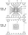
- the carrier film 20 is shown in Figs. 4 and 5.
- Fig. 4 shows the carrier film 20 at a side of the wiring layers 22, that is, at a side facing the semiconductor chip 30.
- Fig. 5 shows an opposite side of the carrier film 20.
- the carrier film 20 is produced, for example, according to the following method:
- a two-layer base member in the form of the polyimide organic insulating film 21 and the metal foil of copper or the like is prepared.
- the organic insulating film 21 has sprocket holes 21-1 formed beforehand in any appropriate manner such as punching.
- the wiring layers 22 of desired shapes are formed on the two-layer base member so as to be properly positioned for connection to the electrode pads 31 of the semiconductor chip 30 through the ball bumps 33.
- each of the wiring layers 22 is connected to the metal material 27 at its one end.
- the other end thereof is connected to an electric-selection pad 22-1.
- the through holes 25 and 26 are formed at the organic insulating film 21 by etching, laser processing or the like.
- the metal material 27 is filled into the through holes 25 and 26 by the electrolytic plating or the like for connection to the wiring layers 22.
- the organic insulating film 21 is etched so as to form positioning holes 21-2.
- the adhesive film 23 is set on the semiconductor chip 30. Subsequently, in Fig. 3(c), the single-point bonder, which is used for the TAB connection, is used so as to achieve the foregoing inner-lead connection after properly positioning between the carrier film 20 and the semiconductor chip 30 temporarily fixed with the adhesive film 23.
- the electric selection (BT) is performed in the same manner as in the normal tape carrier package (TCP), using the electric-selection pads 22-1.
- Fig. 3(f) after indicating an article name, using a laser beam, on a side of the semiconductor chip 30 remote from the carrier film 20, the die or laser is used to cut unnecessary portions of the semiconductor device.
- the chip-size package-type semiconductor device can be obtained as shown in Fig. 3(g).
- the chip-size package-type semiconductor device has been, in general, fabricated in the following manner:
- a size of the adhesive film 23 is limited to a size corresponding to an area defined within the electrode pads 31, that is, not corresponding to all the area of the joint surface of the semiconductor chip 30, so as to avoid overlapping the electrode pads 31.
- a thickness of the adhesive film 23 may be increased so as to expand the adhesive film 23 to the edge of the semiconductor chip 30 upon application of heat and pressure.
- this requires not only the adhesive material excessively, but also the pressing force excessively. This may be a cause of generating cracks in the semiconductor chip 30.
- the adhesive film 23 expands in a circular shape due to the applied pressure, it is rather difficult for the adhesive film 23 to reach corners of the semiconductor chip 30 which is rectangular. This causes the adhesive film 23 to be uneven in thickness after the pressurization thereof.
- the semiconductor chip 30 is bonded to the carrier film 20 in an inclined posture so that the semiconductor device is inclined when mounted onto the external board.
- the connection between the electrode pads 31 and the wiring layers 22 is achieved by applying pressing forces to portions of the carrier film 20 corresponding to the electrode pads 31 using the bonding tool so as to deform such corresponding portions of the carrier film 20.
- a restoring force of the organic insulating film 21 it may be possible that, over a long period of time, the connection between the wiring layer 22 and the electrode pad 31 is spoiled or the wiring layer 22 is separated from the organic insulating film 21.
- the carrier film 20 has the wiring layers 22 on its side confronting the semiconductor chip 30.
- the wiring layers are formed on an opposite side of the carrier film 20.
- wiring layers 22' are covered with a cover coating 29.
- an opening 29-1 is provided at the cover coating 29 for applying Au plating onto the exposed wiring layer 22' and providing bump electrodes by soldering. If a diameter of each opening 29-1 can be set large in light of designing or manufacturing, flux having high viscosity may be applied to each opening 29-1 in advance and a blanked soldering piece can be arranged at each opening 29-1.
- a diameter of the opening 29-1 is very small so that a blanking diameter of the soldering piece should also be set very small.
- a sufficient supply amount of solder can not be obtained.
- a soldering piece 35 having a diameter greater than that of the opening 29-1 is used so as to form it into a ball shape in the opening 29-1. In this case, it may be possible that the ball-shaped solder is out of contact with the wiring layer to cause contact failure and thus can not be used as an external terminal.
- the through hole 25 is formed by the chemical etching or the laser processing using the excimer (KrF) laser.
- the excimer laser is used because it is difficult to achieve the fine processing using the well-known YAG laser.
- the excimer laser can achieve the fine processing, its oscillating tube is expensive and its maintenance cost is high so that it is difficult to use the excimer laser.
- a diameter of the through hole is 50 ⁇ m at minimum. Further, a shape of the through hole is tapered as shown in Fig. 7. Thus, narrowing of the pitches of the through holes is limited.
- a chip-size package-type semiconductor device will be described hereinbelow with reference to Figs. 8(a) to 8(e), Figs. 9(a) to 9(e), and Figs. 10(a) and 10(b).
- a semiconductor wafer 40 is provided.
- the semiconductor wafer 40 is formed with a number of IC's (integrated circuits) and includes a plurality of electrode pads 41 on one side of each of the IC's for connection to the exterior.
- the IC's are in the form before being diced out from the semiconductor wafer 40 as semiconductor chips.
- a region on the foregoing one side of each IC other than at the electrode pads 41 is covered with a passivation film 42 as in the prior art.
- an adhesive layer 43 is formed over all the area of one side of the semiconductor wafer 40 where the electrode pads 41 are formed.
- photosensitive resin such as polyimide or epoxy, is used.
- the adhesive layer 43 is about several micrometers to ten and several micrometers in thickness and formed by the spin coating method.
- the adhesive layer 43 may also be formed by, for example, sticking a film of adhesive on the foregoing side of the semiconductor wafer 40.
- an opening 43-1 is formed through the adhesive layer 43 at a position corresponding to the electrode pad 41.
- the openings 43-1 are formed by the chemical etching, but may also be formed by the laser processing.
- the opening 43-1 is provided per electrode pad 41.
- each opening 43-1 may be formed into an elongate shape for accommodating a plurality of the electrode pads 41.
- the openings 43-1 are arranged at regular pitches of about 50 ⁇ m, each having a width of about several ten micrometers to 100 ⁇ m.
- each opening 43-1 has a width of about 150 ⁇ m.
- electrodes 44 are formed at the openings 43-1, respectively.
- Each electrode 44 is in the form of a metal projection or a metal ball bump.
- the electrode 44 is formed by plating.
- it is known to form an electrode by coating a projection of copper (Cu) with gold (Au).
- Au gold
- the ball bump while the same materials may be used, it is preferable to use a material which is a mixture of gold (Au) with palladium (Pd) added thereto.
- the mixture of gold and palladium is suitable for reducing a diameter of the ball bump, and further achieves an effect of enhancing a joint strength relative to later-described wiring layers on a carrier film as compared with the foregoing materials forming the metal projection.
- Fig. 8(d) that is, the process of providing the electrodes 44, may be omitted depending on a structure of the carrier film.
- Fig. 8(e) the IC's are diced out one by one from the semiconductor wafer 40 as a semiconductor chip 50.
- the electrodes 44 are formed by the ball bumps, the processes in Figs. 8(d) and 8(e) may be reversed in order.
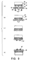
- a carrier film 60 is provided.
- the carrier film 60 includes an organic insulating film 61 and wiring layers 62 formed on one of main surfaces or sides of the organic insulating film 61 confronting the semiconductor chip 50. A carrier film having wiring layers on a side remote from the semiconductor chip 50 will be described later.
- the organic insulating film 61 is formed with through holes 63 at portions corresponding to the electrode pads 41, that is, the electrodes 44, and further formed with through holes 64 at portions for connection to an external board (not shown). These through holes 63 and 64 are formed by the Ar laser processing and the washing processing. The ultrasonic processing may be the most proper as the washing processing.
- a metal material 65 is filled into each through hole 63 by plating, and a metal material 66 is filled into each through hole 64 by plating.
- the metal material 65 filled into the through hole 63 is used as a medium for receiving a bonding tool 70 upon connection between the electrode 44 and the wiring layer 62.
- the metal material 65 may be omitted.
- the metal material 66 filled into the through hole 64 works as an electrode for connection to the external board, and thus is formed as slightly projecting from the through hole 64.
- the material forming the electrode 44 is used for the metal materials 65 and 66.
- connection between the wiring layers 62 of the carrier film 60 and the electrodes 44 of the semiconductor chip 50 is performed.
- this connection is achieved by applying the bonding tool 70 to the metal material 65 so as to firmly attach the wiring layer 62 to the corresponding electrode 44 under pressure.
- the carrier film 60 is pressed upon the semiconductor chip 50 while heating the adhesive layer 43 so that the semiconductor chip 50 and the carrier film 60 are bonded together via the adhesive layer 43.
- the carrier film 60 is cut approximately along the edge of the semiconductor chip 50 so as to provide the semiconductor device of a chip size.
- a ball bump electrode 67 is formed at the tip of each metal material 66 to work as an electrode for connection to the external board.
- solder is mainly used.
- Au or Au added with Pd may also be used therefor.
- the outer surfaces of the chip-size semiconductor device are coated with a coating film 46 formed of a fluororesin coating material using the spin coating method.
- the coating film 46 is provided for preventing the insulation failure due to an invasion of water into the semiconductor device via the joint portion between the semiconductor chip 50 and the carrier film 60 and for preventing an invasion of water into the semiconductor device through the organic insulating film 61.
- the spin coating is performed onto the semiconductor device with the ball bump electrodes 67 being located at the top. Accordingly, the coating film 46 is formed substantially all over the outer surfaces of the semiconductor device except at the upper surface of the semiconductor chip 50.
- the region around the joint portion between the semiconductor chip 50 and the carrier film 60 most requires the reliable sealing, it may be possible to form the coating film only at the region around the joint portion at a lateral side of the semiconductor device.
- the coating film also covers the ball bump electrodes 67.
- connection failure is expected when connecting the ball bump electrodes 67 to the external board.
- a thickness of the coating film formed on each ball bump electrode 67 is small.
- heat and pressure are applied to each ball bump electrode 67 upon connection to the external board, the coating film on the ball bump electrode 67 tends to be broken and thus raises no problem from a practical point of view.
- each ball bump electrode 67 has a spherical shape so that it is difficult for the fluororesin to adhere to the ball bump electrode 67 also from this point of view. This becomes more significant by increasing a height of the ball bump electrode 67.
- the coating film 46 may be formed by dipping the semiconductor device into the fluororesin coating material, instead of using the foregoing spin coating method.
- the adhesive layer 43 By forming the adhesive layer 43 on the semiconductor wafer 40 before cutting the semiconductor chips therefrom, the accurate positioning of the adhesive film relative to the semiconductor chip is not required as opposed to the prior art. Further, the adhesive layer 43 can be provided in a uniform thickness all over the joint surface between the semiconductor chip 50 and the carrier film 60. As a result, the inclination of the semiconductor chip 50 on the carrier film 60 can be prevented, and the sealing at the joint portion between the semiconductor chip 50 and the carrier film 60 can be reliably achieved. Further, the region around the joint portion between the semiconductor chip 50 and the carrier film 60 at the lateral side of the semiconductor device is coated with the coating film 46 so that the sealing is ensured further reliably.
- each electrode 44 is formed so as to slightly project from the corresponding opening 43-1 of the adhesive layer 43.
- a gap is not caused relative to the corresponding wiring layer 62, which would be otherwise caused due to a step corresponding to a thickness of the adhesive layer 43 as in the prior art.
- This means that the connection between the electrode 44 and the wiring layer 62 is achieved without deformation of the organic insulating film 61.
- the connection between the electrode 44 and the wiring layer 62 is not spoiled, and the wiring layer 62 is not separated from the organic insulating film 61, which would be otherwise caused due to deformation of the organic insulating film 61.
- the through holes 63 and 64 of the carrier film 60 are formed by the Ar laser processing and the washing processing.
- the Ar laser processing is lower in running cost as compared with the excimer laser processing and is capable of rendering a shape of each through hole non-tapered, that is, rendering a circumferential wall of each through hole vertical. Further, a diameter of the through hole can be rendered less than 50 ⁇ m. Thus, further narrowing of the pitches of the through holes 63 and 64 can be realized. As appreciated, in the inner-lead connection, narrowing of the pitches of the through holes 63 is important.
- the openings 43-1 of the adhesive layer 43 may also be formed by the Ar laser processing.
- Figs. 11(a) to 11(e) show a modification of the first method.
- the carrier film differs from that in the first method .
- a carrier film 60' includes wiring layers 62' formed on the main side of the organic insulating film 61 opposite to the main side thereof confronting the semiconductor chip 50.
- the organic insulating film 61 is formed with the through holes, that is, the through holes 63, only at portions corresponding to the electrodes 44.
- the through holes 63 are formed by the Ar laser processing and the washing processing as in the first method.
- a metal material 65' which is the same as the metal material 65, is filled by plating as in Fig. 9(a).
- the metal material 65' is filled into each through hole 63 so as to slightly project from the main surface of the organic insulating film 61.
- the wiring layers 62' are coated with a cover coating 68 formed of an insulating material.
- the cover coating 68 is formed with openings 68-1 at portions corresponding to the metal material 65' and at portions for connection to the external board.
- connection between the metal material 65' of the carrier film 60' and each of the electrodes 44 of the semiconductor chip 50 is performed. This connection is achieved by applying the bonding tool 70 to the wiring layer 62' via the opening 68-1 corresponding to the metal material 65' so as to firmly attach the metal material 65' to the corresponding electrode 44 under pressure.
- the carrier film 60' is pressed upon the semiconductor chip 50 while heating the adhesive layer 43 so that the semiconductor chip 50 and the carrier film 60' are bonded together via the adhesive layer 43.
- the carrier film 60' is cut approximately along the edge of the semiconductor chip 50 so as to provide the semiconductor device of a chip size.
- the ball bump electrode 67 is formed at the opening 68-1 to work as an electrode for connection to the external board.
- solder is mainly used.
- Au or Au added with Pd may also be used therefor.
- the outer surfaces of the chip-size semiconductor device are coated with the coating film formed of a fluororesin coating material using the spin coating method.
- a method of forming the bump electrode 67 as described with reference to Fig. 11(e) will be described with reference to Figs. 12(a) to 12(c).
- an electrode pad 69 is formed by Au plating on the wiring layer 62' exposed at the opening 68-1 for connection to the external board.
- the bump electrode 67 is formed the bump electrode 67.
- a commercial solder ribbon 71 in the form of a plate and a commercial special punching jig 72 are used for forming the bump electrode 67.
- the special punching jig 72 has the same function as a normal punch, but differs from the normal punch in that a small projection 72-1 is formed at its tip.
- a portion of the solder ribbon 71 is punched out using the special punching jig 72 so that a solder piece 71-1 punched out from the solder ribbon 71 projects downward at its center so as to have an essentially T-shape in section.
- a pressing force is applied to the T-shaped solder piece 71-1 so as to temporarily joint the center of the solder piece 71-1 to the electrode pad 69.
- the solder piece 71-1 is applied with flux and heated so that, as shown in Fig. 12(c), the solder piece 71-1 is formed into a ball shape so as to be the bump electrode 67.
- Figs. 13(a) and 13(b) show another modification of the first method.
- the carrier film 60' is formed with the wiring layers 62' on the surface of the organic insulating film 61 opposite to the surface thereof confronting the semiconductor chip 50.
- This modification is applied to the case wherein the electrodes 44 are not formed at the openings 43-1 of the adhesive layer 43 in the process in Fig. 8(d) in the first method.
- the metal material 65' is filled into each of the through holes 63 of the carrier film 60'.
- a bump electrode 65-1' is further formed at the tip of the metal material 65'.
- a height of the bump electrode 65-1' is set no less than a thickness of the adhesive layer 43.
- Fig. 14 shows a relationship between a diameter of a material (Au added with Pd) when pressed to another member and a shear strength thereof, wherein the material is used for, for example, the bump electrode or the ball bump electrode.
- the strength becomes greater as an added amount of Pd increases and as a heating temperature increases.
- the adhesive layer 43 described in the first method is formed on the carrier film, and the diced-out semiconductor chip is used.
- the carrier film includes the wiring layers on the surface of the organic insulating film confronting the semiconductor chip, as described with reference to Fig. 9(a).
- a two-layer base member in the form of the organic insulating film 61 (for example, 25 ⁇ m in thickness) and a copper foil 62a (for example, 18 ⁇ m in thickness) stacked on one of main surfaces or sides of the organic insulating film 61 is provided.
- the pattern etching is performed on the copper foil 62a so as to form the wiring layers 62.
- the adhesive layer 43 is formed on a side of the organic insulating film 61 where the wiring layers 62 are formed.
- the adhesive layer 43 is formed by the spin coating method or by sticking the adhesive film as in the foregoing first method.
- the organic insulating film 61 is formed with the through holes 63 and 64, and the adhesive layer 43 is formed with the openings 43-1.
- the through holes 63 and 64 are formed by the Ar laser processing and the washing processing.
- the chemical etching may be used for forming the through holes 63 and 64.
- the openings 43-1 may also be formed by the Ar laser processing or the chemical etching.
- the metal material 65 is filled into the through holes 63 by plating, and the metal material 66 is filled into the through holes 64 by plating.
- a metal material 75 is also filled into the openings 43-1 by plating.
- the filling of the metal material 65 into the through holes 63 may be omitted. Further, the filling of the metal material by plating may be performed only for the through holes of the organic insulating film 61.
- the openings 43-1 of the adhesive layer 43 are provided with ball-shaped bump electrodes each formed of Au or Au added with Pd. As appreciated, these bump electrodes may be provided at the semiconductor chip 50 rather than at the openings 43-1.
- the diced-out semiconductor chip 50 is provided.
- the metal material 75 is connected to each of the electrode pads 41.
- this connection is achieved by applying the bonding tool 70 to the metal material 65 so as to firmly attach the metal material 75 to the corresponding electrode pad 41 under pressure.
- the semiconductor chip 50 and the carrier film 60 are bonded together via the adhesive layer 43 interposed therebetween.
- the bump electrode 67 is provided at the tip of the metal material 66, and the carrier film 60 is cut into a chip size so that the semiconductor device is obtained.
- the outer surfaces of the semiconductor device, particularly the lateral side thereof, are coated with the coating film formed of the fluororesin coating material.
- Figs. 16(a) to 16(g) show a modification of the preferred embodiment.
- the organic insulating film 61 is used so as to locate the wiring layers formed thereon at the side remote from the semiconductor chip.
- the adhesive layer 43 is formed on the main surface opposite to the main surface where the wiring layers 62' are formed.
- the adhesive layer 43 is formed in the same manner as in the first method.
- the plasma ashing or the UV (ultraviolet) irradiation may be applied to the surface of the organic insulating film 61 where the adhesive layer 43 is to be formed, so as to improve the adhesion therebetween.
- the opening 43-1 and the through hole 63 are formed by the Ar laser processing so as to penetrate the adhesive layer 43 and the organic insulating film 61, respectively.
- the through hole 63 and the opening 43-1 are filled with a metal material 76 by plating.
- the tip of the metal material 76 is arranged to project sufficiently from the adhesive layer 43.
- the main surface of the organic insulating film 61 at a side of the wiring layers 62' is coated with the cover coating 68.
- the openings 68-1 are formed by the Ar laser processing at portions corresponding to the metal material 76 and at portions for connection to the external board.
- Fig. 16(e) the semiconductor chip 50 is provided.
- Fig. 16(f) the connection between the metal material 76 and each of the electrode pads 41 of the semiconductor chip 50 is achieved in the same manner as in Fig. 13(b).
- the semiconductor chip 50 and the carrier film 60' are bonded together via the adhesive layer 43 interposed therebetween.
- the carrier film 60' is cut into a chip size, and as shown in Fig. 16(g), the ball bump electrodes 67 are provided at the openings 68-1 of the cover coating 68 for connection to the external board.
- the outer surfaces of the semiconductor device particularly the lateral side thereof, are coated with the coating film formed of the fluororesin coating material.
- the processes in Figs. 16(a) to 16(g) are executed following the process in Fig. 15(b).
- the adhesive layer 43 is formed on the carrier film and bonded to the dice-out semiconductor chip 50.
- the adhesive layer may be formed on a surface of the diced-out semiconductor chip 50 where the electrode pads 41 are formed, so as to cover all the area thereof.
- the openings are formed by the laser processing or the chemical etching at portions of the adhesive layer corresponding to the electrode pads 41. Thereafter, by filling the metal material into these openings by plating or by providing the ball bump electrodes at the openings, the semiconductor chip 50 having the adhesive layer 43 as shown in Fig. 8(e) can be produced.
- Figs. 17(a) and 17(b) show another modification of the preferred embodiment.
- the carrier film 60 is formed with the wiring layers 62 at the side confronting the semiconductor chip 50.
- the filling of the metal material into the openings 43-1 of the adhesive layer 43 by plating is not performed as opposed to the process in Fig. 15(e).
- the semiconductor chip 50 is provided with the bump electrodes 47 on the electrode pads 41.
- Fig. 17(b) after the connection between the wiring layers 62 and the bump electrodes 47 is achieved using the bonding tool 70 in the same manner as in Fig. 15(g), the semiconductor chip 50 and the carrier film 60 are bonded together via the adhesive layer 43 interposed therebetween.
- the processes in Figs. 17(a) and 17(b) are executed instead of the processes in Figs. 15(e) to 15(g). Accordingly, this modification achieves effects similar to those achieved in the preferred embodiment.
- Fig. 18 is a diagram for explaining an example, wherein the directional matching is easily achieved upon mounting the semiconductor device onto the external board.
- a mark for achieving the directional matching is formed by using a portion of the wiring layers 62 of the carrier film.
- the wiring layers of the carrier film are formed by etching the copper foil of the two-layer base member (see Fig. 15(a)) so that the etching regions are limited as small as possible.
- the etching regions are represented by solid lines which are very small.
- the wiring layers tend to remain largely at the center of the carrier film.
- an opening 62-2 is formed at a copper foil which remains as a wiring layer 62-1 at the center of the carrier film during the etching process.
- a user memorizes the opening 62-2 and configuration of the wiring layers around the opening 62-2 in advance.
- the directional matching is achieved by setting an edge 62-3 of the wiring layer 62-1 formed with the opening 62-2 to be an upper side.
- a shape of the opening 62-2 is not circular, but is capable of identifying a particular direction, such as an isosceles triangle, the directional matching can be achieved more easily. Further, if no wiring layers remain at the center of the carrier film, the opening may be formed at the organic insulating film 61. In any case, the foregoing directional matching mark in the form of the opening may apply to any of the foregoing preferred embodiments.
- the processing of the through holes 63 and 64 is not limited to the Ar laser processing, but may be the excimer laser processing or the carbon dioxide laser processing.
- the openings 43-1 of the adhesive layer 43 may be formed by the Ar laser processing.
- the formation of the fluororesin coating film on the outer surfaces of the semiconductor device may be omitted.
Landscapes
- Wire Bonding (AREA)
- Dicing (AREA)
Claims (8)
- Procédé de fabrication d'un dispositif à semi-conducteur comprenant une puce à semi-conducteur (50) ayant des plages d'électrodes (41) sur une surface de celle-ci et un film porteur (60), ledit film porteur (60) comportant un film isolant (61) et des motifs de câblage (62) formés sur une surface principale dudit film isolant (61), le procédé comprenant les étapes consistant à :former une couche adhésive (43) sur une région dudit film porteur (60) correspondant à la totalité de la superficie de ladite surface de la puce à semi-conducteur (50), avec un groupe d'ouvertures (43-1) réalisées dans des régions de ladite couche adhésive (43) correspondant auxdites plages d'électrodes (41) ; etlier l'un à l'autre ladite puce à semi-conducteur (50) et ledit film porteur (60) par l'intermédiaire de ladite couche adhésive (43) ;dans lequel lesdites plages d'électrodes (41) de ladite puce à semi-conducteur (50) et lesdits motifs de câblage (62) dudit film porteur (60) ne sont respectivement connectés à travers ledit groupe d'ouvertures (43-1) qu'après ladite étape de formation de la couche adhésive (43) avec ledit groupe d'ouvertures (43-1) sur ledit film porteur (60).
- Procédé selon la revendication 1, dans lequel ledit groupe d'ouvertures est formé par attaque chimique ou traitement au laser.
- Procédé selon la revendication 1, comportant en outre l'étape consistant, après l'étape de formation dudit groupe d'ouvertures, à former une protubérance métallique ou une bosse métallique en forme de boule à l'emplacement de chaque ouverture dudit groupe d'ouvertures, pour une connexion électrique, ladite protubérance métallique ou ladite bosse métallique en forme de boule faisant saillie par rapport à chaque ouverture dudit groupe d'ouvertures.
- Procédé selon la revendication 3, dans lequel ladite bosse métallique en forme de boule est formée d'Au auquel est ajouté du Pd.
- Procédé selon la revendication 1, dans lequel ledit film isolant est muni de trous traversants permettant de former des passages conducteurs chacun destiné à une connexion entre lesdits motifs de câblage et lesdites plages d'électrodes ou des câblages d'une carte externe, lesdits trous traversants étant formés par un traitement au moyen d'un laser Ar ou par un traitement de lavage.
- Procédé selon la revendication 1, dans lequel ledit film porteur est muni desdits motifs de câblage sur une surface opposée à une autre surface principale qui est en face de ladite puce à semi-conducteur, lesdits motifs de câblage étant revêtus d'un revêtement de protection formé d'un matériau isolant, ledit revêtement de protection étant réalisé avec un groupe supplémentaire d'ouvertures pour la connexion desdits motifs de câblage à des câblages d'une carte externe, ledit groupe supplémentaire d'ouvertures étant muni de bosses respectives en forme de boules, chacune desdites bosses en forme de boules étant formée par poinçonnage d'un morceau de soudure dont la section transversale a pratiquement la forme d'un T dans de la soudure en forme de plaque en utilisant un gabarit de poinçonnage ayant une protubérance à son extrémité, en joignant momentanément ledit morceau de soudure en forme de T à chacun desdits motifs de câblage dans chaque ouverture dudit groupe supplémentaire d'ouvertures, puis en chauffant ledit morceau de soudure en forme de T afin de lui conférer la forme d'une boule.
- Procédé selon la revendication 1, dans lequel une marque permettant une adaptation directionnelle est formée dans une partie centrale dudit film porteur en utilisant lesdits motifs de câblage.
- Procédé selon la revendication 1, comportant en outre l'étape consistant, après l'étape de liaison l'un à l'autre de ladite puce à semi-conducteur et dudit film porteur, par l'intermédiaire de ladite couche adhésive, à revêtir au moins une région de jonction entre ladite puce à semi-conducteur et ledit film porteur sur un côté latéral d'une unité liée de ladite puce à semi-conducteur et dudit film porteur avec un matériau de revêtement à base de résine fluorée.
Applications Claiming Priority (3)
| Application Number | Priority Date | Filing Date | Title |
|---|---|---|---|
| JP6238040A JP2581017B2 (ja) | 1994-09-30 | 1994-09-30 | 半導体装置及びその製造方法 |
| JP23804094 | 1994-09-30 | ||
| JP238040/94 | 1994-09-30 |
Publications (3)
| Publication Number | Publication Date |
|---|---|
| EP0704899A2 EP0704899A2 (fr) | 1996-04-03 |
| EP0704899A3 EP0704899A3 (fr) | 1997-08-20 |
| EP0704899B1 true EP0704899B1 (fr) | 2001-08-01 |
Family
ID=17024283
Family Applications (1)
| Application Number | Title | Priority Date | Filing Date |
|---|---|---|---|
| EP95306887A Expired - Lifetime EP0704899B1 (fr) | 1994-09-30 | 1995-09-29 | Procédé de fabrication d'un boítier pour dispositif semi-conducteur de la taille d'une puce |
Country Status (7)
| Country | Link |
|---|---|
| US (1) | US5897337A (fr) |
| EP (1) | EP0704899B1 (fr) |
| JP (1) | JP2581017B2 (fr) |
| KR (1) | KR100209994B1 (fr) |
| CN (1) | CN1066574C (fr) |
| CA (1) | CA2159243C (fr) |
| DE (1) | DE69521954T2 (fr) |
Cited By (1)
| Publication number | Priority date | Publication date | Assignee | Title |
|---|---|---|---|---|
| US6360556B1 (en) | 1999-11-10 | 2002-03-26 | Shurflo Pump Manufacturing Company, Inc. | Apparatus and method for controlling fluid delivery temperature in a dispensing apparatus |
Families Citing this family (81)
| Publication number | Priority date | Publication date | Assignee | Title |
|---|---|---|---|---|
| US6342434B1 (en) * | 1995-12-04 | 2002-01-29 | Hitachi, Ltd. | Methods of processing semiconductor wafer, and producing IC card, and carrier |
| CN100452376C (zh) * | 1996-07-12 | 2009-01-14 | 富士通株式会社 | 半导体装置 |
| US6881611B1 (en) * | 1996-07-12 | 2005-04-19 | Fujitsu Limited | Method and mold for manufacturing semiconductor device, semiconductor device and method for mounting the device |
| EP1189271A3 (fr) * | 1996-07-12 | 2003-07-16 | Fujitsu Limited | Plaquettes de circuit et montage des dispositifs semiconducteurs au dessus de ces plaquettes |
| TW345710B (en) * | 1996-07-31 | 1998-11-21 | Hitachi Chemical Co Ltd | Chip supporting substrate for semiconductor package, semiconductor package and process for manufacturing semiconductor package |
| DE69730629T2 (de) | 1996-12-26 | 2005-02-03 | Matsushita Electric Industrial Co., Ltd., Kadoma | Leiterplatte und Elektronikkomponente |
| JP3328157B2 (ja) * | 1997-03-06 | 2002-09-24 | シャープ株式会社 | 液晶表示装置 |
| DE19754372A1 (de) * | 1997-03-10 | 1998-09-24 | Fraunhofer Ges Forschung | Chipanordnung und Verfahren zur Herstellung einer Chipanordnung |
| JPH1174413A (ja) * | 1997-07-01 | 1999-03-16 | Sony Corp | リードフレームとリードフレームの製造方法と半導体装置と半導体装置の組立方法と電子機器 |
| JPH1126631A (ja) * | 1997-07-02 | 1999-01-29 | Matsushita Electric Ind Co Ltd | 半導体装置とその製造方法 |
| JP3526731B2 (ja) * | 1997-10-08 | 2004-05-17 | 沖電気工業株式会社 | 半導体装置およびその製造方法 |
| KR100475338B1 (ko) * | 1997-10-10 | 2005-05-24 | 삼성전자주식회사 | 와이어본더를이용한칩스케일패키지및제조방법 |
| JPH11163022A (ja) * | 1997-11-28 | 1999-06-18 | Sony Corp | 半導体装置、その製造方法及び電子機器 |
| JPH11214435A (ja) * | 1998-01-26 | 1999-08-06 | Sharp Corp | 半導体装置およびその製造方法 |
| JP3481117B2 (ja) * | 1998-02-25 | 2003-12-22 | 富士通株式会社 | 半導体装置及びその製造方法 |
| JP3876953B2 (ja) | 1998-03-27 | 2007-02-07 | セイコーエプソン株式会社 | 半導体装置及びその製造方法、回路基板並びに電子機器 |
| FR2778308B1 (fr) * | 1998-04-30 | 2006-05-26 | Schlumberger Systems & Service | Procede de realisation d'un composant electronique et composant electronique |
| KR100266698B1 (ko) * | 1998-06-12 | 2000-09-15 | 김영환 | 반도체 칩 패키지 및 그 제조방법 |
| US6103552A (en) * | 1998-08-10 | 2000-08-15 | Lin; Mou-Shiung | Wafer scale packaging scheme |
| DE59915167D1 (de) | 1998-08-21 | 2010-06-24 | Infineon Technologies Ag | Verfahren zur herstellung von integrierten schaltkreisen |
| SE512906C2 (sv) * | 1998-10-02 | 2000-06-05 | Ericsson Telefon Ab L M | Förfarande vid lödning av ett halvledarchip samt RF-power transistor för genomförande därav |
| JP3661444B2 (ja) * | 1998-10-28 | 2005-06-15 | 株式会社ルネサステクノロジ | 半導体装置、半導体ウエハ、半導体モジュールおよび半導体装置の製造方法 |
| JP2000138313A (ja) * | 1998-10-30 | 2000-05-16 | Shinko Electric Ind Co Ltd | 半導体装置及びその製造方法 |
| US6331450B1 (en) * | 1998-12-22 | 2001-12-18 | Toyoda Gosei Co., Ltd. | Method of manufacturing semiconductor device using group III nitride compound |
| JP2000311921A (ja) * | 1999-04-27 | 2000-11-07 | Sony Corp | 半導体装置およびその製造方法 |
| US6338980B1 (en) * | 1999-08-13 | 2002-01-15 | Citizen Watch Co., Ltd. | Method for manufacturing chip-scale package and manufacturing IC chip |
| JP2001094005A (ja) * | 1999-09-22 | 2001-04-06 | Oki Electric Ind Co Ltd | 半導体装置及び半導体装置の製造方法 |
| FR2799306B1 (fr) * | 1999-10-04 | 2003-09-19 | Gemplus Card Int | Procede d'isolation de puce de circuit integre par depot de matiere sur la face active |
| FR2800198B1 (fr) * | 1999-10-26 | 2002-03-29 | Gemplus Card Int | Procede de protection de puces de circuit integre par aspiration sous vide |
| US6271057B1 (en) * | 1999-11-19 | 2001-08-07 | Advanced Semiconductor Engineering, Inc. | Method of making semiconductor chip package |
| US6723620B1 (en) * | 1999-11-24 | 2004-04-20 | International Rectifier Corporation | Power semiconductor die attach process using conductive adhesive film |
| US6388335B1 (en) * | 1999-12-14 | 2002-05-14 | Atmel Corporation | Integrated circuit package formed at a wafer level |
| US6710454B1 (en) * | 2000-02-16 | 2004-03-23 | Micron Technology, Inc. | Adhesive layer for an electronic apparatus having multiple semiconductor devices |
| DE10014379A1 (de) * | 2000-03-23 | 2001-10-11 | Infineon Technologies Ag | Verfahren und Vorrichtung zum Verbinden mindestens eines Chips mit einer Umverdrahtungsanordnung |
| JP3597754B2 (ja) | 2000-04-24 | 2004-12-08 | Necエレクトロニクス株式会社 | 半導体装置及びその製造方法 |
| JP2001308220A (ja) * | 2000-04-24 | 2001-11-02 | Nec Corp | 半導体パッケージ及びその製造方法 |
| US7214566B1 (en) * | 2000-06-16 | 2007-05-08 | Micron Technology, Inc. | Semiconductor device package and method |
| JP2002005951A (ja) * | 2000-06-26 | 2002-01-09 | Denso Corp | 半導体力学量センサ及びその製造方法 |
| JP2002050716A (ja) * | 2000-08-02 | 2002-02-15 | Dainippon Printing Co Ltd | 半導体装置及びその作製方法 |
| CN100378977C (zh) * | 2000-11-14 | 2008-04-02 | 联测科技股份有限公司 | 无晶片承载件的半导体装置及其制法 |
| JP3621908B2 (ja) * | 2001-10-11 | 2005-02-23 | 松下電器産業株式会社 | ベアチップ実装方法および実装システム |
| JP2003249465A (ja) * | 2002-02-26 | 2003-09-05 | Seiko Epson Corp | 半導体装置及びその製造方法 |
| US6908784B1 (en) * | 2002-03-06 | 2005-06-21 | Micron Technology, Inc. | Method for fabricating encapsulated semiconductor components |
| US6964881B2 (en) * | 2002-08-27 | 2005-11-15 | Micron Technology, Inc. | Multi-chip wafer level system packages and methods of forming same |
| US6903442B2 (en) * | 2002-08-29 | 2005-06-07 | Micron Technology, Inc. | Semiconductor component having backside pin contacts |
| CN100374000C (zh) * | 2002-10-04 | 2008-03-05 | 电子科学工业公司 | 在小型元件载体的弹性遮罩中形成尺寸精确的狭槽的方法 |
| US7388294B2 (en) * | 2003-01-27 | 2008-06-17 | Micron Technology, Inc. | Semiconductor components having stacked dice |
| US6982190B2 (en) * | 2003-03-25 | 2006-01-03 | Id Solutions, Inc. | Chip attachment in an RFID tag |
| US6841883B1 (en) * | 2003-03-31 | 2005-01-11 | Micron Technology, Inc. | Multi-dice chip scale semiconductor components and wafer level methods of fabrication |
| JP4308608B2 (ja) * | 2003-08-28 | 2009-08-05 | 株式会社ルネサステクノロジ | 半導体装置 |
| TWI254995B (en) * | 2004-01-30 | 2006-05-11 | Phoenix Prec Technology Corp | Presolder structure formed on semiconductor package substrate and method for fabricating the same |
| US7180134B2 (en) * | 2004-01-30 | 2007-02-20 | Taiwan Semiconductor Manufacturing Company, Ltd. | Methods and structures for planar and multiple-gate transistors formed on SOI |
| TWI236742B (en) * | 2004-03-02 | 2005-07-21 | Kingtron Electronics Co Ltd | Manufacturing method of film carrier |
| DE102004062212A1 (de) * | 2004-12-23 | 2006-07-13 | Texas Instruments Deutschland Gmbh | Elektronische Vorrichtung, Chipkontaktierungsverfahren und Kontaktierungsvorrichtung |
| US8456015B2 (en) * | 2005-06-14 | 2013-06-04 | Cufer Asset Ltd. L.L.C. | Triaxial through-chip connection |
| US7767493B2 (en) | 2005-06-14 | 2010-08-03 | John Trezza | Post & penetration interconnection |
| US7687400B2 (en) * | 2005-06-14 | 2010-03-30 | John Trezza | Side stacking apparatus and method |
| US7838997B2 (en) * | 2005-06-14 | 2010-11-23 | John Trezza | Remote chip attachment |
| US7786592B2 (en) * | 2005-06-14 | 2010-08-31 | John Trezza | Chip capacitive coupling |
| US7946331B2 (en) * | 2005-06-14 | 2011-05-24 | Cufer Asset Ltd. L.L.C. | Pin-type chip tooling |
| US20060281303A1 (en) * | 2005-06-14 | 2006-12-14 | John Trezza | Tack & fuse chip bonding |
| CN100346467C (zh) * | 2005-07-19 | 2007-10-31 | 钰创科技股份有限公司 | 电路重布线方法及电路结构 |
| JP2007067272A (ja) * | 2005-09-01 | 2007-03-15 | Nitto Denko Corp | Tab用テープキャリアおよびその製造方法 |
| JP4692260B2 (ja) * | 2005-12-12 | 2011-06-01 | 株式会社デンソー | 半導体力学量センサ装置およびその製造方法 |
| TWI285424B (en) * | 2005-12-22 | 2007-08-11 | Princo Corp | Substrate including a multi-layer interconnection structure, methods of manufacturing and recycling the same, method of packaging electronic devices by using the same, and method of manufacturing an interconnection device |
| CN1996143B (zh) * | 2006-01-06 | 2010-12-08 | 日月光半导体制造股份有限公司 | 压合于晶圆上的干膜的清洗流程 |
| US8051557B2 (en) * | 2006-03-31 | 2011-11-08 | Princo Corp. | Substrate with multi-layer interconnection structure and method of manufacturing the same |
| US20070281460A1 (en) * | 2006-06-06 | 2007-12-06 | Cubic Wafer, Inc. | Front-end processed wafer having through-chip connections |
| US7670874B2 (en) * | 2007-02-16 | 2010-03-02 | John Trezza | Plated pillar package formation |
| US8829663B2 (en) * | 2007-07-02 | 2014-09-09 | Infineon Technologies Ag | Stackable semiconductor package with encapsulant and electrically conductive feed-through |
| US7838424B2 (en) * | 2007-07-03 | 2010-11-23 | Taiwan Semiconductor Manufacturing Company, Ltd. | Enhanced reliability of wafer-level chip-scale packaging (WLCSP) die separation using dry etching |
| PL2192969T3 (pl) * | 2007-08-28 | 2015-09-30 | Commw Scient Ind Res Org | Artykuł do ekstrahowania komponentu ze strumienia płynu, sposoby i systemy zawierające go |
| JP5712615B2 (ja) * | 2008-11-25 | 2015-05-07 | 住友ベークライト株式会社 | 電子部品パッケージおよび電子部品パッケージの製造方法 |
| JP4724222B2 (ja) * | 2008-12-12 | 2011-07-13 | 株式会社東芝 | 発光装置の製造方法 |
| JP5420274B2 (ja) | 2009-03-02 | 2014-02-19 | パナソニック株式会社 | 半導体装置及びその製造方法 |
| US8709874B2 (en) * | 2010-08-31 | 2014-04-29 | Advanpack Solutions Pte Ltd. | Manufacturing method for semiconductor device carrier and semiconductor package using the same |
| US10881833B2 (en) | 2013-07-09 | 2021-01-05 | Truecath Inc. | Intravascular catheter insertion device |
| US10136917B2 (en) | 2013-07-09 | 2018-11-27 | Sean S. Farley | Intravascular catheter insertion device |
| US11944766B2 (en) | 2013-07-09 | 2024-04-02 | Truecath Inc | Intravascular catheter insertion device |
| TWI569368B (zh) * | 2015-03-06 | 2017-02-01 | 恆勁科技股份有限公司 | 封裝基板、包含該封裝基板的封裝結構及其製作方法 |
| US11932203B2 (en) | 2021-08-04 | 2024-03-19 | Cnh Industrial America Llc | Step with integrated water tank for agricultural vehicle |
Citations (1)
| Publication number | Priority date | Publication date | Assignee | Title |
|---|---|---|---|---|
| JPH02229445A (ja) * | 1989-03-01 | 1990-09-12 | Nitto Denko Corp | フィルムキャリアおよび半導体装置 |
Family Cites Families (12)
| Publication number | Priority date | Publication date | Assignee | Title |
|---|---|---|---|---|
| JPS55130133A (en) * | 1979-03-30 | 1980-10-08 | Hitachi Ltd | Semiconductor device |
| JPS57112038A (en) * | 1980-12-29 | 1982-07-12 | Matsushima Kogyo Co Ltd | Semiconductor device |
| US5030308A (en) * | 1986-07-14 | 1991-07-09 | National Starch And Chemical Investment Holding Corporation | Method of bonding a semiconductor chip to a substrate |
| EP0260490A1 (fr) * | 1986-08-27 | 1988-03-23 | Kabushiki Kaisha Toshiba | Couche de liaison pour un composant électronique, et méthode pour lier ledit composant utilisant cette couche |
| US5097841A (en) * | 1988-09-22 | 1992-03-24 | Terumo Kabushiki Kaisha | Disposable pressure transducer and disposable pressure transducer apparatus |
| JP2737953B2 (ja) * | 1988-09-29 | 1998-04-08 | 三菱マテリアル株式会社 | 金バンプ用金合金細線 |
| US5151769A (en) * | 1991-04-04 | 1992-09-29 | General Electric Company | Optically patterned RF shield for an integrated circuit chip for analog and/or digital operation at microwave frequencies |
| US5350947A (en) * | 1991-11-12 | 1994-09-27 | Nec Corporation | Film carrier semiconductor device |
| US5286679A (en) * | 1993-03-18 | 1994-02-15 | Micron Technology, Inc. | Method for attaching a semiconductor die to a leadframe using a patterned adhesive layer |
| WO1994024694A1 (fr) * | 1993-04-14 | 1994-10-27 | Amkor Electronics, Inc. | Interconnexion d'une puce de circuit integree et d'un substrat |
| US5434751A (en) * | 1994-04-11 | 1995-07-18 | Martin Marietta Corporation | Reworkable high density interconnect structure incorporating a release layer |
| JP2833996B2 (ja) * | 1994-05-25 | 1998-12-09 | 日本電気株式会社 | フレキシブルフィルム及びこれを有する半導体装置 |
-
1994
- 1994-09-30 JP JP6238040A patent/JP2581017B2/ja not_active Expired - Fee Related
-
1995
- 1995-09-25 US US08/533,205 patent/US5897337A/en not_active Expired - Fee Related
- 1995-09-27 CA CA002159243A patent/CA2159243C/fr not_active Expired - Fee Related
- 1995-09-29 DE DE69521954T patent/DE69521954T2/de not_active Expired - Fee Related
- 1995-09-29 EP EP95306887A patent/EP0704899B1/fr not_active Expired - Lifetime
- 1995-09-29 KR KR1019950033149A patent/KR100209994B1/ko not_active Expired - Fee Related
- 1995-09-30 CN CN95118615A patent/CN1066574C/zh not_active Expired - Fee Related
Patent Citations (1)
| Publication number | Priority date | Publication date | Assignee | Title |
|---|---|---|---|---|
| JPH02229445A (ja) * | 1989-03-01 | 1990-09-12 | Nitto Denko Corp | フィルムキャリアおよび半導体装置 |
Non-Patent Citations (1)
| Title |
|---|
| PATENT ABSTRACTS OF JAPAN vol. 14, no. 541 (E - 1007) 29 November 1990 (1990-11-29) * |
Cited By (1)
| Publication number | Priority date | Publication date | Assignee | Title |
|---|---|---|---|---|
| US6360556B1 (en) | 1999-11-10 | 2002-03-26 | Shurflo Pump Manufacturing Company, Inc. | Apparatus and method for controlling fluid delivery temperature in a dispensing apparatus |
Also Published As
| Publication number | Publication date |
|---|---|
| CA2159243C (fr) | 2000-06-13 |
| EP0704899A2 (fr) | 1996-04-03 |
| CN1066574C (zh) | 2001-05-30 |
| JPH08102474A (ja) | 1996-04-16 |
| US5897337A (en) | 1999-04-27 |
| CA2159243A1 (fr) | 1996-03-31 |
| KR100209994B1 (ko) | 1999-07-15 |
| DE69521954D1 (de) | 2001-09-06 |
| JP2581017B2 (ja) | 1997-02-12 |
| CN1128901A (zh) | 1996-08-14 |
| DE69521954T2 (de) | 2001-11-15 |
| EP0704899A3 (fr) | 1997-08-20 |
| KR960012397A (ko) | 1996-04-20 |
Similar Documents
| Publication | Publication Date | Title |
|---|---|---|
| EP0704899B1 (fr) | Procédé de fabrication d'un boítier pour dispositif semi-conducteur de la taille d'une puce | |
| US6593648B2 (en) | Semiconductor device and method of making the same, circuit board and electronic equipment | |
| US5717252A (en) | Solder-ball connected semiconductor device with a recessed chip mounting area | |
| US7129584B2 (en) | Elimination of RDL using tape base flip chip on flex for die stacking | |
| US7129586B2 (en) | Flip chip packaging structure and related packaging method | |
| US8604348B2 (en) | Method of making a connection component with posts and pads | |
| KR100241573B1 (ko) | 반도체 웨이퍼 | |
| KR100555241B1 (ko) | 능동 표면상에 포스트를 구비한 전자적 구성요소 패키지 | |
| US20020127778A1 (en) | Tape ball grid array semiconductor package structure and assembly process | |
| US7534652B2 (en) | Microelectronic elements with compliant terminal mountings and methods for making the same | |
| JP3848368B2 (ja) | 半導体接続素子のリードの形成 | |
| US7202113B2 (en) | Wafer level bumpless method of making a flip chip mounted semiconductor device package | |
| KR100309962B1 (ko) | 테이프캐리어및그제조방법 | |
| US20020028535A1 (en) | Circuit, method of adhering an integrated circuit device to a substrate, and method of forming a circuit | |
| US6323434B1 (en) | Circuit board and production method thereof | |
| JP3350454B2 (ja) | 半導体集積回路装置およびその製造方法並びに製造装置 | |
| JP3827978B2 (ja) | 半導体装置の製造方法 | |
| JP2004207293A (ja) | 半導体装置及びその製造方法、回路基板並びに電子機器 | |
| JPH11224918A (ja) | 半導体装置及びその製造方法 | |
| US20040256719A1 (en) | MEMS micro-cap wafer level chip scale package | |
| KR100249539B1 (ko) | 반도체 칩 및 그 제조방법 | |
| JP2000299399A (ja) | 半導体装置 | |
| JP2519243B2 (ja) | 半導体装置 | |
| JPH11330146A (ja) | 半導体装置およびその製造方法ならびにその製造方法で使用するテープキャリヤ |
Legal Events
| Date | Code | Title | Description |
|---|---|---|---|
| PUAI | Public reference made under article 153(3) epc to a published international application that has entered the european phase |
Free format text: ORIGINAL CODE: 0009012 |
|
| AK | Designated contracting states |
Kind code of ref document: A2 Designated state(s): DE FR GB IT NL |
|
| PUAL | Search report despatched |
Free format text: ORIGINAL CODE: 0009013 |
|
| AK | Designated contracting states |
Kind code of ref document: A3 Designated state(s): DE FR GB IT NL |
|
| 17P | Request for examination filed |
Effective date: 19970723 |
|
| 17Q | First examination report despatched |
Effective date: 19981217 |
|
| GRAG | Despatch of communication of intention to grant |
Free format text: ORIGINAL CODE: EPIDOS AGRA |
|
| GRAG | Despatch of communication of intention to grant |
Free format text: ORIGINAL CODE: EPIDOS AGRA |
|
| GRAH | Despatch of communication of intention to grant a patent |
Free format text: ORIGINAL CODE: EPIDOS IGRA |
|
| GRAH | Despatch of communication of intention to grant a patent |
Free format text: ORIGINAL CODE: EPIDOS IGRA |
|
| GRAA | (expected) grant |
Free format text: ORIGINAL CODE: 0009210 |
|
| AK | Designated contracting states |
Kind code of ref document: B1 Designated state(s): DE FR GB IT NL |
|
| REF | Corresponds to: |
Ref document number: 69521954 Country of ref document: DE Date of ref document: 20010906 |
|
| ET | Fr: translation filed | ||
| REG | Reference to a national code |
Ref country code: GB Ref legal event code: IF02 |
|
| PLBE | No opposition filed within time limit |
Free format text: ORIGINAL CODE: 0009261 |
|
| STAA | Information on the status of an ep patent application or granted ep patent |
Free format text: STATUS: NO OPPOSITION FILED WITHIN TIME LIMIT |
|
| 26N | No opposition filed | ||
| REG | Reference to a national code |
Ref country code: GB Ref legal event code: 732E |
|
| NLS | Nl: assignments of ep-patents |
Owner name: NEC ELECTRONICS CORPORATION |
|
| REG | Reference to a national code |
Ref country code: FR Ref legal event code: TP |
|
| PGFP | Annual fee paid to national office [announced via postgrant information from national office to epo] |
Ref country code: FR Payment date: 20050823 Year of fee payment: 11 |
|
| PGFP | Annual fee paid to national office [announced via postgrant information from national office to epo] |
Ref country code: NL Payment date: 20050915 Year of fee payment: 11 |
|
| PGFP | Annual fee paid to national office [announced via postgrant information from national office to epo] |
Ref country code: DE Payment date: 20050922 Year of fee payment: 11 |
|
| PGFP | Annual fee paid to national office [announced via postgrant information from national office to epo] |
Ref country code: GB Payment date: 20050928 Year of fee payment: 11 |
|
| PGFP | Annual fee paid to national office [announced via postgrant information from national office to epo] |
Ref country code: IT Payment date: 20060930 Year of fee payment: 12 |
|
| PG25 | Lapsed in a contracting state [announced via postgrant information from national office to epo] |
Ref country code: NL Free format text: LAPSE BECAUSE OF NON-PAYMENT OF DUE FEES Effective date: 20070401 |
|
| PG25 | Lapsed in a contracting state [announced via postgrant information from national office to epo] |
Ref country code: DE Free format text: LAPSE BECAUSE OF NON-PAYMENT OF DUE FEES Effective date: 20070403 |
|
| GBPC | Gb: european patent ceased through non-payment of renewal fee |
Effective date: 20060929 |
|
| NLV4 | Nl: lapsed or anulled due to non-payment of the annual fee |
Effective date: 20070401 |
|
| REG | Reference to a national code |
Ref country code: FR Ref legal event code: ST Effective date: 20070531 |
|
| PG25 | Lapsed in a contracting state [announced via postgrant information from national office to epo] |
Ref country code: GB Free format text: LAPSE BECAUSE OF NON-PAYMENT OF DUE FEES Effective date: 20060929 |
|
| PG25 | Lapsed in a contracting state [announced via postgrant information from national office to epo] |
Ref country code: FR Free format text: LAPSE BECAUSE OF NON-PAYMENT OF DUE FEES Effective date: 20061002 |
|
| PG25 | Lapsed in a contracting state [announced via postgrant information from national office to epo] |
Ref country code: IT Free format text: LAPSE BECAUSE OF NON-PAYMENT OF DUE FEES Effective date: 20070929 |