EP0704924B1 - Dielektrisches Filter - Google Patents
Dielektrisches Filter Download PDFInfo
- Publication number
- EP0704924B1 EP0704924B1 EP95306254A EP95306254A EP0704924B1 EP 0704924 B1 EP0704924 B1 EP 0704924B1 EP 95306254 A EP95306254 A EP 95306254A EP 95306254 A EP95306254 A EP 95306254A EP 0704924 B1 EP0704924 B1 EP 0704924B1
- Authority
- EP
- European Patent Office
- Prior art keywords
- resonant lines
- dielectric
- outer conductor
- open
- filter
- Prior art date
- Legal status (The legal status is an assumption and is not a legal conclusion. Google has not performed a legal analysis and makes no representation as to the accuracy of the status listed.)
- Expired - Lifetime
Links
- 239000004020 conductor Substances 0.000 claims description 87
- 230000008030 elimination Effects 0.000 claims description 30
- 238000003379 elimination reaction Methods 0.000 claims description 30
- 238000012216 screening Methods 0.000 claims description 11
- 230000010363 phase shift Effects 0.000 claims description 10
- 238000010586 diagram Methods 0.000 description 33
- 230000008878 coupling Effects 0.000 description 10
- 238000010168 coupling process Methods 0.000 description 10
- 238000005859 coupling reaction Methods 0.000 description 10
- 239000003990 capacitor Substances 0.000 description 8
- 238000010295 mobile communication Methods 0.000 description 8
- 239000000758 substrate Substances 0.000 description 4
- 230000005540 biological transmission Effects 0.000 description 2
- 238000004891 communication Methods 0.000 description 2
- 230000000694 effects Effects 0.000 description 1
- 238000005516 engineering process Methods 0.000 description 1
- 238000003780 insertion Methods 0.000 description 1
- 230000037431 insertion Effects 0.000 description 1
- 238000012986 modification Methods 0.000 description 1
- 230000004048 modification Effects 0.000 description 1
Images



Classifications
-
- H—ELECTRICITY
- H01—ELECTRIC ELEMENTS
- H01P—WAVEGUIDES; RESONATORS, LINES, OR OTHER DEVICES OF THE WAVEGUIDE TYPE
- H01P1/00—Auxiliary devices
- H01P1/20—Frequency-selective devices, e.g. filters
- H01P1/201—Filters for transverse electromagnetic waves
- H01P1/205—Comb or interdigital filters; Cascaded coaxial cavities
- H01P1/2056—Comb filters or interdigital filters with metallised resonator holes in a dielectric block
-
- H—ELECTRICITY
- H01—ELECTRIC ELEMENTS
- H01P—WAVEGUIDES; RESONATORS, LINES, OR OTHER DEVICES OF THE WAVEGUIDE TYPE
- H01P1/00—Auxiliary devices
- H01P1/20—Frequency-selective devices, e.g. filters
Definitions
- This invention relates to a dielectric band elimination filter. More particularly, this invention relates to a dielectric band elimination filter adapted for use in a mobile communication apparatus such as a portable telephone.
- a prior art single-stage dielectric band elimination filter (BEF) is formed with a dielectric resonator 111 and a coupling capacitor C e 112 connected in series through a connector terminal 113.
- Its frequency-attenuation characteristic is shown in Fig. 27.
- Fig. 28 is a block diagram of a prior art mobile communication apparatus such as a portable telephone, and a dielectric band elimination filter, as described above, is used in the transmitter circuit inside its duplexer D 1 .
- the transmitter frequency f TX and the receiver frequency f RX of this communication apparatus are indicated in the diagram of Fig. 27. It is adjusted such that the receiver frequency f RX and the trap frequency f T of the dielectric BEF match each other.
- Fig. 29 a general prior art two-stage dielectric BEF is shown in Fig. 29.
- R indicates a resonator
- C e indicates a trap capacitor
- C t indicates a parallel capacitor
- L indicates an inductor serving as a quarter-wavelength phase shifter
- numerals 121, 122, 123, 124 respectively indicate a case cover, a connector terminal, an inductor pattern substrate, and a common substrate.
- FIG. 31 shows the frequency-attenuation characteristic of this dielectric BEF, and also indicates the transmitter frequency f TX and the receiver frequency f RX when this filter is used in the transmitter side of the duplexer D 1 of the communication apparatus shown in Fig. 28.
- the receiver frequency f RX and the trap frequency f T of the filter are adjusted to match each other.
- dielectric band elimination filter comprising:
- a small interdigital filter is disclosed in JP-A-61-167201 having plural cylindrical metallised throughholes in a dielectric block having a conductive film thereon. One end of each hole has a non-conductive portion provided on the surface of the dielectric block. Adjacent conductive through-holes have their non-conductive portion at opposite ends.
- the invention provides a dielectric band elimination filter comprising a dielectric block having outer surfaces including two mutually opposite first and second end surfaces; an outer conductor covering portions of said outer surfaces; and two mutually coupled resonant lines formed extending in said dielectric block between said end surfaces, each of said resonant lines having an open end which is not in contact with said outer conductor and a shorted end which is in contact with said outer conductor, said open and shorted ends of said two resonant lines are oppositely oriented; characterised in that said open end of one of said two resonant lines is unconnected to an outer circuit and said open end of said other of said resonant lines is connected to an outside circuit.
- the invention also provides a dielectric band elimination filter as above, wherein said dielectric block has a plurality of single-stage band elimination filters each having two interdigitally coupled resonant lines extending between said first and second end surfaces inside throughholes through said block, each mutually adjacent pair of said single-stage band elimination filters being interdigitally coupled or combline-coupled to each other with phase shift of ⁇ /2.
- Each single-stage band elimination filter may be structured as described above, each of its two resonant lines having an open end and a shorted end, and their open and shorted ends being oriented oppositely.
- Each open end may be formed at one of the end surfaces of the dielectric block, being connected to an electrode on the end surface and insulated from the outer conductor, or at an annular conductor-free area formed on the inner surface of the corresponding throughhole.
- the resonant lines for forming the plurality of single-stage band elimination filters may be arranged in various ways. They may be arranged in two horizontal rows (the upper and lower rows) and many vertical columns, those one the upper and lower rows in each column forming a single-stage filter. With this arrangement of the resonant lines, all of the resonant lines on the upper row may be arranged to have their open ends pointing towards one of the end surfaces of the dielectric block, those on the lower row pointing to the other end surface. Alternatively, the resonant lines may be so arranged that the open ends of two mutually adjacent resonant lines on the same row are always oriented in opposite directions. Screening electrodes may be inserted between resonant lines which are next to each other on the same row.
- pairs of resonant lines forming single-stage band elimination filters need not all be arranged in the same direction.
- Two such filters with horizontally arranged resonant line may sandwich one with vertically arranged resonant line inside a horizontally elongated dielectric block with an upwardly protruding center part for forming therein one of the resonant lines for the vertically arranged filter.
- the throughholes for containing the resonant lines may have a flattened shape such that the dielectric block can be made thinner.
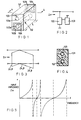
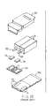
- FIG. 1 shows a single-stage dielectric BEF according to a first embodiment of this invention, formed by a combination of two resonant lines.
- a rectangular dielectric block 101 has two circular cylindrical throughholes 102a, 103a formed near each other from one end surface to the opposite end surface.
- Inner conductors are formed on the inner surfaces of the throughholes 102a, 103a.
- the inner conductor inside throughhole 102a is connected to a rectangular electrode 102b on one of the end surfaces (first end surface) of the dielectric block 101.
- the inner conductor inside throughhole 103a is connected to another rectangular electrode 103b on the other end surface (second end surface) of the dielectric block 101.
- the outer surfaces of the dielectric block 101 are substantially entirely covered by an outer conductor, excluding conductor-free (or dielectric-exposing) areas 102c, 103c surrounding the electrodes 102b, 103b.
- the inner conductor inside throughhole 102a is connected to the outer conductor on the second end surface of the dielectric block 101 to form a quarter-wavelength resonant line 102.
- the inner conductor inside through- hole 103a is connected to the outer conductor on the first end surface of the dielectric block 101 to form another quarter-wavelength resonant line 103.
- the conductor-free areas 102c, 103c serve as open ends of these quarter-wavelength resonant lines 102, 103. It is to be noted that these two resonant lines 102, 103 are in a point-symmetric relationship with respect to the centre of the dielectric block 101.
- Fig. 2 shows the circuit structure of the filter described above, its equivalent circuit diagram being shown in Fig. 3, and Fig. 4 is a sectional view of the filter taken along line 4-4 in Fig. 1 to show how equivalent capacitors are formed.
- self-capacitance C 11 per unit length is formed between each of the resonant lines 102, 103 and the outer conductor, and mutual capacitance C 12 is formed between the two resonant lines 101, 103.
- Z in indicates the input impedance.
- the equivalent circuit diagram shows a parallel connection of the even-mode characteristic impedance Z e and a series connection of the coupling characteristic impedance Z k and the even-mode characteristic impedance Z e between the input (output) and the ground.
- Fig. 5 shows the input impedance characteristic of this filter
- Fig. 6 shows its frequency-attenuation characteristic.
- the solid line is for this invention; the broken line is for a prior art example shown in Fig. 27.
- Fig. 6 shows that increased attenuation is obtained by the present invention both in regions (indicated by double-headed arrows) on the higher frequency and lower frequency sides of the trap frequency.
- a single-stage dielectric BEF according to this invention having such a frequency-attenuation characteristic is used in the transmitter circuit of the duplexer D 1 of the mobile communication apparatus shown in Fig. 28, it becomes possible to eliminate the isolator I 1 for stopping invading waves from the antenna A 1 into the transmitter side of the duplexer D 1 because sufficient attenuation is obtained on the lower frequency side of the trap frequency. Since attenuation is obtained both on the lower and higher frequency sides of the trap frequency, furthermore, the BPF B 1 for attenuating waves with unwanted frequencies generated by the mixer M 1 on the transmitter side can be either eliminated or replaced by a smaller, less costly BPF with fewer stages.
- the dielectric BEF according to this invention is formed with a single dielectric block providing its trap circuit by a mutually coupling pair of resonant lines, there is no need for a coupling capacitor to be connected or any connector terminal. In other words, the number of component parts can be reduced.
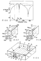
- Fig. 7 shows another single-stage dielectric BEF according to a second embodiment of this invention, which is similar to the one described above except that the electrodes 103b for resonant line 103 and the outer conductor are removed from the second end surface.
- Components which are substantially identical or function substantially identically to those of the filter shown in Fig. 1 are indicated by the same numerals and are not repetitively described below.
- the filter according to the second embodiment shown in Fig. 7 functions substantially like the first embodiment and is advantageous in that the number of electrode patterns is reduced and hence that it can be produced at a reduced cost.
- Fig. 8 shows still another single-stage dielectric BEF according to a third embodiment of this invention, which is similar to the first embodiment described above with reference to Fig. 1 and of which components substantially identical or at least similar to those of the first embodiment are indicated in Fig. 8 by the same numerals.
- the third embodiment is different from the first embodiment in that two inner conductors (first and second inner conductors) are formed inside one of the throughholes (104a).
- One end of the first inner conductor is connected to the outer conductor on the first end surface of the dielectric block 101.
- One end of the second inner conductor is connected to the outer conductor on the second end surface of the dielectric block 101.
- annular conductor-free (or dielectric-exposing) area 104b formed on the inner surface of the throughhole 104a near the second end surface.
- the conductor-free area 104b may be formed adjacent to the second end surface (there being no second inner conductor), as a variation of the third embodiment.
- a single-stage filter according to the third embodiment of the invention also has functions similar to the first embodiment and is advantageous wherein it has better shielding effects because the outer surfaces of the dielectric block 1 are completely covered by the outer conductor except at the input and output portions.
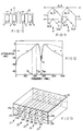
- Fig. 9 shows a two-stage dielectric BEF according to a fourth embodiment of this invention, comprising a rectangular dielectric block 10 having four circular cylindrical throughholes 1a, 2a, 3a, 4a formed therethrough near one another from one end surface to the opposite end surface of the block 10.
- Inner conductors are formed on the inner surfaces of the throughholes 1a, 2a, 3a, 4a.
- the inner conductor inside throughhole 2a is connected to an electrode 2b on one of the end surfaces (first end surface) of the block 10.
- the inner conductor inside throughhole 3a is connected to another electrode 3b on the other end surface (second end surface) of the block 10.
- the outer surfaces of the block 10 are substantially entirely covered by an outer conductor except conductor-free (or dielectric-exposing) areas 2c, 3c surrounding the electrodes 2b, 3b.
- annular conductor-free (or dielectric-exposing) area 1c is formed on the inner surface near the second end surface.
- another annular conductor-free (or dielectric-exposing) area 4c is formed on the inner surface near the first end surface.
- the inner conductors inside throughholes 1a, 3a, 4a are connected to the outer conductor on the first end surface, and the inner conductors inside throughholes 1a, 2a, 4a are connected to the outer conductor on the second end surface such that interdigital resonator lines 1-4 are formed by these throughholes 1a-4a.
- the conductor-free areas 1c, 2c, 3c, 4c serve as open ends of the resonant lines 1-4.
- annular conductor-free areas 1c, 4c may be formed adjacent respectively to the second end surface and to the first end surface of the block 10, as discussed with reference to the filter according to the third embodiment of the invention shown in Fig. 8.
- resonant lines 1, 2 couple to each other interdigitally to together form a one-stage BEF 11, and resonant lines 3, 4 similarly couple to each other interdigitally to together form another single-stage BEF 12.
- These two BEFs 11, 12 are coupled to each other through a quarter-wavelength phase shifter formed between the resonant lines 2, 3 such that a two-stage dielectric BEF is formed as a whole.
- a dielectric BEF thus formed is capable of providing attenuation on both higher and lower frequency sides of the trap frequency, the electrodes 2b, 3b of the resonant lines 2, 3 serving as input and output lines.
- Each single-stage BEF 11, 12 is represented as a parallel connection of a series-connected parallel branch comprising (Z k , ⁇ ) and (Z e , ⁇ ) and another parallel branch comprising (Z e , ⁇ ).
- the filter shown in Fig. 9 is represented as a combination of two such single-stage BEFs connected through transmission lines (Z k , ⁇ ).
- Fig. 12 shows that attenuation at the trap frequency f T is approximately the same but that increased attenuation is obtained by the present invention both on lower and higher frequency regions (shown by arrows) with respect to the trap frequency f T .
- an LC-type ⁇ -circuit is adapted to serve both as a quarter-wavelength phase shifter and a low pass filter for obtaining attenuation outside the band.
- a low pass filter With an LC-type low pass filter, however, attenuation cannot be obtained on the lower frequency side, and attenuation on the higher frequency side is not sufficiently great, as compared to what is achievable by the present invention.
- a two-stage dielectric BEF having such frequency-attenuation characteristic is used in the transmitter circuit in the duplexer D 1 of the mobile communication apparatus shown in Fig. 28, it is possible to eliminate the isolator I 1 for stopping invading waves from the antenna A 1 into the transmitter side of the duplexer D 1 because sufficient attenuation is obtained on the lower frequency side of the trap frequency. Since attenuation is obtained in fact both on the lower and higher frequency sides of the trap frequency, the BPF B 1 for attenuating waves of unwanted frequencies generated by the mixer M 1 on the transmitter side can be either eliminated or replaced by a smaller, less costly BPF with fewer stages.
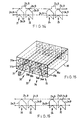
- Fig. 13 shows a five-stage combline-coupled dielectric BEF according to a fifth embodiment of this invention, comprising a rectangular dielectric block 20 having a total of ten circular cylindrical throughholes formed therethrough near one another from one end surface to the opposite end surface of the block 20, arranged geometrically in two horizontal rows such that resonant lines 21a-25a are formed in the five throughholes of the upper row and resonant lines 21b-25b are formed in the five throughholes of the lower row.
- the resonant lines 21a-25a of the upper row each have a shorted end and the resonant lines 21b-25b of the lower row each have an open end.
- the resonant lines 21a-25a of the upper row each have an open end and the resonant lines 21b-25b of the lower row each have a shorted end.
- the outer surfaces of the dielectric block 20 are substantially entirely covered by an outer conductor excluding the open end surfaces. Inner conductors are formed on the inner surfaces of the throughholes forming the resonant lines 21a-25a, 21b-25b.
- Each of pairs of upper-row and lower-row resonant lines 21a with 21b, 22a with 22b, 23a with 23b, 24a with 24b, 25a with 25b couples interdigitally to form one-stage BEFs 21, 22, 23, 24, 25.
- Each mutually adjacent pair of these one-stage BEFs is combline-coupled to each other according to a known mechanism.
- Input to and output from this dielectric filter are effected through the resonant lines 21b and 25b.
- An equivalent circuit diagram of this filter is shown in Fig.
- Fig. 15 shows a five-stage interdigitally coupled dielectric BEF according to a sixth embodiment of this invention, comprising a rectangular dielectric block 30 having a total of ten circular cylindrical throughholes formed therethrough near one another from one end surface to the opposite end surface of the block 30, arranged geometrically in two horizontal rows, resonant lines 31a-35a being formed in the five throughholes of the upper row and resonant lines 31b-35b being formed in the five throughholes of the lower row.
- Inner conductors are formed on the inner surfaces of these ten throughholes for the resonant lines 31a-35a, 31b-35b.
- Resonant lines 31a, 32b, 33a, 34b, 35a each have a shorted end on one of the end surfaces (first end surface) of the dielectric block 30 and an open end on the other end surface (second end surface).
- Resonant lines 31b, 32a, 33b, 34a, 35b each have an open end on the first end surface and a shorted end on the second end surface.
- the outer surfaces of the dielectric block 30 are substantially entirely covered by an outer conductor except at the aforementioned open ends.
- Each of the pairs of upper and lower resonant lines 31a with 31b, 32a with 32b, 33a with 33b, 34a with 34b, 35a with 35b couples to each other interdigitally to form a single-stage BEF 31, 32, 33, 34, 35.
- Each mutually adjacent pair of these one-stage BEFs is interdigitally coupled, as shown in the equivalent circuit diagram of Fig. 16. Since this equivalent circuit diagram is similar to the one explained above in Fig. 11, it is not repetitively explained here. Input to and output from this filter are effected through resonant lines 31b and 35b.
- Fig. 17 shows another five-stage combline-coupled dielectric BEF according to a seventh embodiment of this invention.
- This filter is similar to the one described above with reference to Fig. 13 except that screening electrodes 41 connected to the outer conductor are provided between each mutually adjacent pair of the resonant lines 21a-25a of the upper row.
- this filter is identical to the one shown in Fig. 13. Therefore, same numerals as used in Fig. 13 are used in Fig. 17 to indicate identical components.
- Fig. 18 shows a three-stage interdigitally coupled dielectric BEF according to an eighth embodiment of this invention, comprising a rectangular dielectric block 50 having a total of six circular cylindrical throughholes formed therethrough near one another from one end surface to the opposite end surface of the block 50, arranged geometrically in two horizontal rows, resonant lines 51a-53a being formed in the throughholes of the upper row and resonant lines 51b-53b being formed in the throughholes of the lower row.
- Inner conductors are formed on the inner surfaces of these throughholes for the resonant lines 51a-53a, 51b-53b.
- the inner conductors of the resonant lines 51b, 52a, 53b are connected respectively to electrodes 51c, 52c, 53c on one of the end surfaces (first end surface) of the block 50 and to an outer conductor on the other end surface (second end surface).
- the inner conductors of the resonant lines 51a, 52b, 53a are connected respectively to electrodes 51d, 52d, 53d on the second end surface and to the outer conductor on the first end surface.
- the outer conductor covers the outer surfaces of the dielectric block 50 substantially entirely except conductor-free (or dielectric-exposing) areas 50a surrounding the electrodes 51c-53c, 51d-53d.
- Screening electrodes 54 are provided between horizontally adjacent pairs of resonant lines of the upper row 51a with 52a, 52a with 53a for preventing coupling therebetween.
- Each pair of vertically adjacent resonant lines 51a with 51b, 52a with 53b, 53a with 53b of the upper and lower rows is interdigitally coupled to form single-stage BEFs 51, 52, 53.
- Mutually adjacent pairs of the resonant lines of the lower row 51b with 52b, 52b with 53b are interdigitally coupled with phase shift of ⁇ /2 such that the three single-stage BEFs 51, 52, 53 together form an interdigitally coupled dielectric BEF.
- Fig. 19 is its circuit structure diagram
- Fig. 20 is its equivalent circuit diagram.
- Fig. 21 shows another three-stage interdigitally coupled dielectric BEF according to a ninth embodiment of this invention, comprising a rectangular dielectric block 60 having a protrusion and a total of six throughholes formed therethrough with inner conductors formed on the inner surfaces of these throughholes so as to provide six resonant lines 61a-63a, 61b-63b near one another.
- Resonant lines 62a and 62b are vertically adjacent to each other and interdigitally coupled to each other to together form a single-stage BEF 62. Pairs of resonant lines 61a with 61b, 63a with 63b are horizontally adjacent and interdigitally coupled to each other to form single-stage BEFs 61 and 63, respectively.
- the inner conductors of the resonant lines 61b, 62a, 63a are connected respectively to electrodes 61c, 62c, 63c on one end surface (first end surface) of the dielectric block 60 and to an outer conductor on the opposite end surface (second end surface).
- the inner conductors of resonant lines 61a, 62b, 63b are connected respectively to electrodes 61d, 62d, 63d on the second end surface and to the outer conductor on the first end surface.
- the outer conductor covers the outer surfaces of the dielectric block 60 substantially entirely except at conductor-free (or dielectric-exposing) areas 60a around the electrodes 61c-63c, 61d-63d.
- the three single-stage BEFs 61, 62, 63 are interdigitally coupled with phase shift of ⁇ /2 as in the preceding embodiment of the invention, forming an interdigitally coupled dielectric BEF.
- the circuit structure diagram and the equivalent circuit diagram of this filter are substantially the same as shown in Figs. 19 and 20.
- Fig. 22 shows still another three-stage interdigitally coupled dielectric BEF according to a tenth embodiment of this invention, comprising a rectangular dielectric block 70 having a total of six resonator-forming throughholes formed therethrough from one end surface to the opposite end surface of the block 70, arranged geometrically near one another so as to provide three circular cylindrical resonant lines 71a-73a on an upper row and three others 71b-73b on an lower row.
- Inner conductors are formed on the inner surfaces of these resonator-forming throughholes.
- the inner conductors of the resonant lines 71b, 73b are respectively connected to electrodes 71c, 73c on one of the end surfaces (first end surface) of the dielectric block 70. Both ends of the inner conductors of the resonant lines 71a-73a, 71b-73b are connected to an outer conductor except at the ends of the resonant lines 71b, 73b on the first end surface.
- the outer conductor covers the outer surfaces of the dielectric block 70 substantially entirely except at conductor-free (or dielectric-exposing) areas 70a surrounding the electrodes 71c, 73c.
- the resonant lines 71a, 72b, 73a are respectively provided with annular conductor-free (or dielectric-exposing) areas 71d, 72d, 73d near the opposite end surface (second end surface) of the dielectric block 70.
- the resonant line 72a is similarly provided with an annular conductor-free (or dielectric-exposing) area 72c near the first end surface of the dielectric block 70.
- These annular areas 71d-73d, 72c serve not only to divide the corresponding inner conductors into two parts but also as open ends of the corresponding resonant lines.
- these annular areas 71d-73d, 72c may each be formed adjacent to (rather than near) the first or second end surface.
- Screening throughholes 70b are formed through the dielectric block 70 parallel to the aforementioned resonator-forming throughholes between the resonant lines 71a and 72a and also between the resonant lines 72a and 73a on the upper row. These screening throughholes 70b contain screening electrodes therein, in contact with the outer conductor at both ends so as to prevent coupling between the resonant lines 71a and 72a and between the resonant lines 72a and 73a.
- the vertically adjacent pairs of resonant lines 71a with 71b, 72a with 72b, 73a with 73b are interdigitally coupled to each other to form three single-stage BEFs 71, 72, 73.
- Fig. 19 shows its circuit structure diagram
- Fig. 20 shows its equivalent circuit diagram
- Fig. 23 shows a six-stage interdigitally coupled BEF according to an eleventh embodiment of this invention, comprising a rectangular dielectric block 80 having a total of twelve circular cylindrical throughholes formed from one end surface to the opposite end surface of the dielectric block 80, geometrically arranged in three horizontal rows and four vertical columns, having inner conductors formed on the inner surfaces of the throughholes so as to serve as resonant lines 81a-86a, 81b-86b.
- Resonant lines 81a, 82b, 83a, 84a, 85b, 86a each have an open end on one of the end surfaces (first end surface) of the dielectric block 80 and a shorted end on the opposite end surface (second end surface) of the dielectric block 80.
- Resonant lines 81b, 82a, 83b, 84b, 85a, 86b each have a shorted end on the first end surface and an open end on the second end surface.
- the outer surfaces of the dielectric block 80 are substantially entirely covered by an outer conductor except at the aforementioned open ends. Screening electrodes 80a connected to the outer conductor are provided between mutually adjacent pair of resonant lines 81b and 86a of the lower row and between mutually adjacent pair of resonant lines 82b and 85a of the middle row.
- Horizontally adjacent pairs of resonant lines 81a and 81b, 82a and 82b, 83a and 83b, 84a and 84b, 85a and 85b, 86a and 86b couple to each other interdigitally within themselves to form single-stage BEFs 81, 82, 83, 84, 85, 86, respectively.
- Mutually adjacent pairs of these single-stage BEFs 81-86 couple interdigitally each other with phase shifts of ⁇ /2 and thereby form altogether an interdigitally coupled dielectric BEF. Input to and output from this filter are effected through the resonant lines 81b and 86a.
- throughholes whether for forming resonant lines therein or for containing a screening electrode, need not be circular in cross-section. If the through-holes are made in the shape of a horizontally elongated rectangle of flattened ellipse, the filter as a whole can be made thinner.
- a dielectric BEF sufficient attenuation can be obtained both on the lower and higher frequency sides of the trap frequency by a dielectric BEF according to this invention. If such a filter is used in a mobile communication apparatus such as a portable telephone, it is possible to simplify the circuit structure by eliminating the isolator and the BPF which used to be necessary. Since the number of component parts becomes reduced, the production cost is also reduced. If the number of components to be soldered is reduced, reliability is improved, individual variations in characteristics are reduced among the products, and the yield is increased.
Landscapes
- Physics & Mathematics (AREA)
- Electromagnetism (AREA)
- Control Of Motors That Do Not Use Commutators (AREA)
Claims (16)
- Ein dielektrisches Bandsperrfilter mit folgenden Merkmalen:einem dielektrischen Block (101), der äußere Oberflächen aufweist, die eine erste und eine zweite Endoberfläche aufweisen, die sich gegenüberliegen;einem äußeren Leiter, der Abschnitte der äußeren Oberflächen bedeckt; undzwei gegenseitig gekoppelten Resonanzleitungen (102, 103), die sich zwischen den Endoberflächen in dem dielektrischen Block (101) erstreckend gebildet sind, wobei jede der Resonanzleitungen (102, 103) ein Leerlaufende, das sich nicht in einem Kontakt mit dem äußeren Leiter befindet, und ein Kurzschlußende aufweist, das sich in einem Kontakt mit dem äußeren Leiter befindet, wobei die Leerlaufenden und die Kurzschlußenden der zwei Resonanzleitungen entgegengesetzt ausgerichtet sind; dadurch gekennzeichnet, daß das Leerlaufende einer der zwei Resonanzleitungen nicht mit einer äußeren Schaltung verbunden ist, und daß das Leerlaufende der anderen der Resonanzleitungen mit einer äußeren Schaltung verbunden ist.
- Das dielektrische Filter gemäß Anspruch 1, bei dem eine der Endoberflächen einen leiterfreien Bereich (102c, 103c) aufweist, und sich das Leerlaufende von einer der Resonanzleitungen in dem leiterfreien Bereich befindet.
- Das dielektrische Filter gemäß Anspruch 1, bei dem die Leerlaufenden der Resonanzleitungen (102, 103) mit Endoberflächenelektroden (102b, 103b) verbunden sind, die an den Endoberflächen gebildet sind, und die von dem äußeren Leiter isoliert sind.
- Das dielektrische Filter gemäß Anspruch 1, bei dem der dielektrische Block (101) Durchgangslöcher (102a, 103b) aufweist, die durch denselben zwischen den Endoberflächen gebildet sind, und bei dem sich die Leerlaufenden in leiterfreien Bereichen an inneren Oberflächen der Durchgangslöcher (102a, 103a) befinden.
- Das dielektrische Filter gemäß Anspruch 1, bei dem der dielektrische Block (10; 20) eine Mehrzahl von Einstufen-Bandsperrfiltern (21 - 25) aufweist, die jeweils zwei interdigital gekoppelte Resonanzleitungen (1 - 4; 21a - 25a, 21b - 25b) aufweisen, die sich zwischen der ersten und der zweiten Endoberfläche innerhalb der Durchgangslöcher (1a - 4a) durch den Block erstrecken, wobei jedes benachbarte Paar der Einstufen-Bandsperrfilter mit einer Phasenverschiebung von π/2 miteinander interdigital gekoppelt oder kammleitungsgekoppelt ist.
- Das dielektrische Filter gemäß Anspruch 5, das ferner einen äußeren Leiter aufweist, der Abschnitte von äußeren Oberflächen des dielektrischen Blocks (10; 20) bedeckt, wobei jede der zwei interdigital gekoppelten Resonanzleitungen (1 - 4; 21a - 25a, 21b - 25b) ein Leerlaufende, das von dem äußeren Leiter isoliert ist, und ein Kurzschlußende aufweist, das mit dem äußeren Leiter verbunden ist, wobei die Leerlaufenden und die Kurzschlußenden der zwei Resonanzleitungen von jedem der Einstufen-Bandsperrfilter (21 - 25) entgegengesetzt ausgerichtet sind, wobei das Leerlaufende von einer der zwei Resonanzleitungen von jedem der Einstufen-Bandsperrfilter an einer der Endoberflächen gebildet ist, wobei sich das Leerlaufende der anderen der zwei Resonanzleitungen von jedem der Einstufen-Bandsperrfilter in einem ringförmigen leiterfreien Bereich befindet, der an der inneren Oberfläche eines entsprechenden der Durchgangslöcher (1a - 4a) gebildet ist.
- Das dielektrische Filter gemäß Anspruch 5 oder Anspruch 6, bei dem sich die Durchgangslöcher (1a - 4a) horizontal erstrecken, horizontal angeordnet sind und eine horizontal längliche Querschnittsform aufweisen.
- Das dielektrische Filter gemäß Anspruch 5, das ferner einen äußeren Leiter aufweist, der Abschnitte von äußeren Oberflächen des dielektrischen Blocks (20) bedeckt, wobei die Resonanzleitungen (21a - 25a, 21b-25b) in zwei horizontalen Reihen angeordnet sind, die aus einer oberen und einer unteren Reihe und mindestens zwei vertikalen Spalten bestehen, wobei jede der Resonanzleitungen ein Leerlaufende, das von dem äußeren Leiter isoliert ist, und ein Kurzschlußende aufweist, das mit dem äußeren Leiter verbunden ist, wobei die Leerlaufenden und die Kurzschlußenden der Resonanzleitungen in der oberen Reihe an der ersten bzw. der zweiten Endoberfläche gebildet sind, wobei die Leerlaufenden und die Kurzschlußenden der Resonanzleitungen in der unteren Reihe an der zweiten bzw. der ersten Endoberfläche gebildet sind, wobei das Paar der Resonanzleitungen in jeder Spalte miteinander interdigital gekoppelt ist, um ein Einstufen-Bandsperrfilter (21 - 25) zu bilden, wobei jedes gegenseitig benachbarte Paar der Einstufen-Bandsperrfilter mit einer Phasenverschiebung von π/2 zwischen denselben miteinander kammleitungsgekoppelt ist.
- Das dielektrische Filter gemäß Anspruch 5, das ferner einen äußeren Leiter aufweist, der Abschnitte von äußeren Oberflächen des dielektrischen Blocks (30) bedeckt, wobei jede der Resonanzleitungen (31a - 35a, 31b - 35b) ein Leerlaufende, das von dem äußeren Leiter isoliert ist, und ein Kurzschlußende aufweist, das mit dem äußeren Leiter verbunden ist, wobei die Resonanzleitungen in zwei horizontalen Reihen angeordnet sind, die aus einer oberen und einer unteren Reihe und mindestens zwei vertikalen Spalten bestehen, wobei die Leerlaufenden von jedem Paar von Resonanzleitungen, die horizontal oder vertikal nahe zueinander liegen, sich auf unterschiedlichen der Endoberflächen befinden, wobei das Paar der Resonanzleitungen in jeder Spalte miteinander interdigital gekoppelt ist, um ein Einstufen-Bandsperrfilter (31 - 35) zu bilden, wobei jedes gegenseitig benachbarte Paar von Einstufen-Band-sperrfiltern mit einer Phasenverschiebung von π/2 zwischen denselben miteinander interdigital gekoppelt ist.
- Das dielektrische Filter gemäß Anspruch 5, das ferner einen äußeren Leiter aufweist, der Abschnitte von äußeren Oberflächen des dielektrischen Blocks (20) bedeckt, wobei die Resonanzleitungen (21a - 25a, 21b-25b) in zwei horizontalen Reihen angeordnet sind, die aus einer oberen und einer unteren Reihe und mindestens zwei vertikalen Spalten bestehen, wobei jede der Resonanzleitungen ein Leerlaufende, das von dem äußeren Leiter isoliert ist, und ein Kurzschlußende aufweist, das mit dem äußeren Leiter verbunden ist, wobei die Leerlaufenden und die Kurzschlußenden der Resonanzleitungen in der oberen Reihe an der ersten bzw. der zweiten Endoberfläche gebildet sind, wobei die Leerlaufenden und die Kurzschlußenden der Resonanzleitungen in der unteren Reihe an der zweiten bzw. der ersten Endoberfläche gebildet sind, wobei das Paar von Resonanzleitungen in jeder Spalte miteinander interdigital gekoppelt ist, um ein Einstufen-Bandsperrfilter (21 - 25) zu bilden, wobei eine Abschirmelektrode (41), die mit dem äußeren Leiter verbunden ist, zwischen jedem von gegenseitig benachbarten Paaren der Resonanzleitungen in der oberen Reihe vorgesehen ist, wobei jedes gegenseitig benachbarte Paar der Einstufen-Bandsperrfilter mit einer Phasenverschiebung von π/2 zwischen denselben miteinander interdigital gekoppelt ist.
- Das dielektrische Filter gemäß Anspruch 5, das ferner einen äußeren Leiter aufweist, der Abschnitte von äußeren Oberflächen des dielektrischen Blocks (50) bedeckt, wobei jede der Resonanzleitungen (51a - 53a, 51b - 53b) ein Leerlaufende, das mit einer Leerlaufelektrode (51c - 53c) verbunden ist, die von dem äußeren Leiter isoliert ist, und ein Kurzschlußende aufweist, das mit dem äußeren Leiter verbunden ist, wobei die Resonanzleitungen in zwei horizontalen Reihen angeordnet sind, die aus einer oberen und einer unteren Reihe und mindestens zwei vertikalen Spalten bestehen, wobei sich die Leerlaufenden von jedem Paar von Resonanzleitungen, die sich horizontal oder vertikal nahe zueinander befinden, auf unterschiedlichen Endoberflächen befinden, wobei das Paar der Resonanzleitungen in jeder Spalte miteinander interdigital gekoppelt ist, um ein Einstufen-Bandsperrfilter (51-53) zu bilden, wobei eine Abschirmelektrode (54), die mit dem äußeren Leiter verbunden ist, zwischen jedem von gegenseitig benachbarten Paaren der Resonanzleitungen in der oberen Reihe vorgesehen ist.
- Das dielektrische Filter gemäß Anspruch 5, das ferner einen äußeren Leiter aufweist, der Abschnitte der äußeren Oberflächen des dielektrischen Blocks (60) bedeckt, wobei der dielektrische Block ferner einen sich horizontal erstreckenden unteren Teil und einen nach oben vorstehenden Mittelteil aufweist, wobei jede der Resonanzleitungen (61a - 63a, 61b - 63b) ein Leerlaufende, das von dem äußeren Leiter isoliert ist, und ein Kurzschlußende aufweist, das mit dem äußeren Leiter verbunden ist, wobei die Resonanzleitungen mindestens drei Paare bilden, wobei zwei der Resonanzleitungen von jedem der Paare miteinander interdigital gekoppelt sind, um ein Einstufen-Bandsperrfilter (61-63) zu bilden, wobei sich die Leerlaufenden und die Kurzschlußenden der Resonanzleitungen von jedem der Paare auf unterschiedlichen der Endoberflächen befinden, wobei eines der Paare vertikal angeordnet ist, wobei sich eine der Resonanzleitungen in dem nach oben vorstehenden Mittelteil befindet, und sich die andere der Resonanzleitungen darunter befindet, wobei zwei andere der Paare horizontal angeordnet sind und auf beiden Seiten des vertikal angeordneten Paars in dem sich horizontal erstreckenden Teil des dielektrischen Blocks gebildet sind.
- Das dielektrische Filter gemäß Anspruch 5, das ferner einen äußeren Leiter aufweist, der Abschnitte von äußeren Oberflächen des dielektrischen Blocks (70) bedeckt, wobei die Resonanzleitungen (71a - 73a, 71b - 73b) in zwei horizontalen Reihen angeordnet sind, die aus einer oberen und einer unteren Reihe und mindestens drei vertikalen Spalten bestehen, die Endspalten und innere Spalten dazwischen aufweisen, wobei jede der Resonanzleitungen ein Leerlaufende und ein Kurzschlußende aufweist, wobei das Paar der Resonanzleitungen in jeder Spalte miteinander interdigital gekoppelt ist, um ein Einstufen-Bandsperrfilter (71-73) zu bilden, wobei die Leerlaufenden und die Kurzschlußenden des interdigital gekoppelten Paars von jedem der Einstufen-Bandsperrfilter an gegenüberliegenden der Endoberflächen gebildet sind, wobei die Leerlaufenden der Resonanzleitungen in den Endspalten in der unteren Reihe jeweils mit einem Leerlaufanschluß verbunden sind, der auf einer der Endoberflächen des dielektrischen Blocks gebildet ist, wobei die Leerlaufenden der Resonanzleitungen in den Endspalten in der oberen Reihe und in den inneren Spalten jeweils in einem ringförmigen leiterfreien Bereich (71d - 73d) gebildet sind, der an einer inneren Oberfläche eines entsprechenden der Durchgangslöcher gebildet ist.
- Das dielektrische Filter gemäß Anspruch 13, bei dem sich die Reihen horizontal erstrecken und die Durchgangslöcher eine horizontal längliche Querschnittsform aufweisen.
- Das dielektrische Filter gemäß Anspruch 5, das ferner einen äußeren Leiter aufweist, der Abschnitte von äußeren Oberflächen des dielektrischen Blocks (80) bedeckt, wobei jede der Resonanzleitungen (81a - 86a, 81b - 86b) ein Leerlaufende, das von dem äußeren Leiter isoliert ist, und ein Kurzschlußende aufweist, das mit dem äußeren Leiter verbunden ist, wobei die Resonanzleitungen in mindestens drei horizontalen Reihen und mindestens vier vertikalen Spalten angeordnet sind, wobei sich die Leerlaufenden von jedem Paar von Resonanzleitungen, die sich horizontal oder vertikal nahe zueinander befinden, auf unterschiedlichen der Endoberflächen befinden, wobei Abschirmelektroden (84) zwischen ausgewählten Paaren der Resonanzleitungen vorgesehen sind, die sich nahe zueinander befinden, wobei Paare der Resonanzleitungen, die sich horizontal nahe zueinander befinden, miteinander interdigital gekoppelt sind, um Einstufen-Bandsperrfilter (81 - 86) zu bilden.
- Das dielektrische Filter gemäß einem der Ansprüche 8, 9, 10, 11, 12 und 15, bei dem die Durchgangslöcher eine horizontal längliche Querschnittsform aufweisen.
Applications Claiming Priority (12)
| Application Number | Priority Date | Filing Date | Title |
|---|---|---|---|
| JP23182994 | 1994-09-27 | ||
| JP23182994A JP3282405B2 (ja) | 1994-09-27 | 1994-09-27 | 誘電体フィルタ |
| JP231830/94 | 1994-09-27 | ||
| JP23183094 | 1994-09-27 | ||
| JP23183094 | 1994-09-27 | ||
| JP231829/94 | 1994-09-27 | ||
| JP10140095 | 1995-04-25 | ||
| JP07101400A JP3085139B2 (ja) | 1994-09-27 | 1995-04-25 | 誘電体フィルタ |
| JP101400/95 | 1995-04-25 | ||
| JP469443/95 | 1995-06-06 | ||
| US469443 | 1995-06-06 | ||
| US08/469,443 US5712604A (en) | 1994-09-27 | 1995-06-06 | Dielectric filter including at least one band elimination filter |
Publications (2)
| Publication Number | Publication Date |
|---|---|
| EP0704924A1 EP0704924A1 (de) | 1996-04-03 |
| EP0704924B1 true EP0704924B1 (de) | 2000-01-26 |
Family
ID=27468920
Family Applications (1)
| Application Number | Title | Priority Date | Filing Date |
|---|---|---|---|
| EP95306254A Expired - Lifetime EP0704924B1 (de) | 1994-09-27 | 1995-09-07 | Dielektrisches Filter |
Country Status (2)
| Country | Link |
|---|---|
| EP (1) | EP0704924B1 (de) |
| KR (1) | KR100201707B1 (de) |
Families Citing this family (5)
| Publication number | Priority date | Publication date | Assignee | Title |
|---|---|---|---|---|
| JP3461420B2 (ja) * | 1996-05-15 | 2003-10-27 | アルプス電気株式会社 | 誘電体フィルタ |
| JPH10145110A (ja) * | 1996-11-05 | 1998-05-29 | Murata Mfg Co Ltd | 複合誘電体フィルタ |
| TW409458B (en) * | 1998-11-03 | 2000-10-21 | Samsung Electro Mech | Dielectric filter |
| US6670867B2 (en) * | 2000-10-26 | 2003-12-30 | Sei-Joo Jang | Dielectric filter for filtering out unwanted higher order frequency harmonics and improving skirt response |
| EP3716395A1 (de) | 2019-03-26 | 2020-09-30 | Nokia Solutions and Networks Oy | Vorrichtung für hochfrequenzsignale und verfahren zur herstellung solch einer vorrichtung |
Family Cites Families (4)
| Publication number | Priority date | Publication date | Assignee | Title |
|---|---|---|---|---|
| JPS61167201A (ja) * | 1985-01-21 | 1986-07-28 | Tdk Corp | インタ−デイジタルフイルタ− |
| JPH0644681B2 (ja) * | 1988-11-21 | 1994-06-08 | 国際電気株式会社 | 帯域阻止フィルタ |
| CA2037262A1 (en) * | 1990-03-02 | 1991-09-03 | Hiroyuki Sogo | Dielectric resonator and a filter using same |
| JP2750389B2 (ja) * | 1990-10-30 | 1998-05-13 | 三洋電機株式会社 | 誘電体フィルタ |
-
1995
- 1995-09-07 EP EP95306254A patent/EP0704924B1/de not_active Expired - Lifetime
- 1995-09-27 KR KR1019950032112A patent/KR100201707B1/ko not_active Expired - Lifetime
Also Published As
| Publication number | Publication date |
|---|---|
| EP0704924A1 (de) | 1996-04-03 |
| KR960012603A (ko) | 1996-04-20 |
| KR100201707B1 (en) | 1999-06-15 |
Similar Documents
| Publication | Publication Date | Title |
|---|---|---|
| EP0788179B1 (de) | Dielektrisches Filter | |
| EP0840390B1 (de) | Filter für mehrere Bandpässe | |
| US6577211B1 (en) | Transmission line, filter, duplexer and communication device | |
| KR0167806B1 (ko) | 안테나 공용기 | |
| KR100321104B1 (ko) | 유전체필터및유전체듀플렉서 | |
| JP3580162B2 (ja) | 誘電体フィルタ、誘電体デュプレクサ、通信機装置 | |
| US5712604A (en) | Dielectric filter including at least one band elimination filter | |
| KR100276012B1 (ko) | 유전체필터와 송수신듀플렉서 및 통신기기 | |
| KR100401969B1 (ko) | 유전체 필터, 유전체 듀플렉서 및 통신 장치 | |
| JP2002158512A (ja) | 誘電体共振器、誘電体フィルタ、誘電体デュプレクサ、および通信装置 | |
| EP0704924A1 (de) | Dielektrisches Filter | |
| US6549093B2 (en) | Dielectric filter, duplexer, and communication apparatus incorporating the same | |
| CN114788087B (zh) | 多层带通滤波器 | |
| US5563561A (en) | Dielectric block apparatus having two opposing coaxial resonators separated by an electrode free region | |
| EP0347774B1 (de) | Isolierungsschaltung und darin verwendetes dielektrisches Filter | |
| US5652555A (en) | Dielectrical filters having resonators at a trap frequency where the even/odd mode impedances are both zero | |
| EP0707352B1 (de) | Dielektrisches Filter | |
| JP2025515739A (ja) | フィルターモジュール及びこれを含むアンテナモジュール | |
| KR20050051567A (ko) | 안테나 공용기 | |
| JP3521805B2 (ja) | 誘電体フィルタ、複合誘電体フィルタ、アンテナ共用器および通信装置 | |
| KR100304267B1 (ko) | 유전체 필터 장치, 듀플렉서 및 통신기 장치 | |
| EP1294042B1 (de) | Dielektrisches Filter, dielektrischer Duplexer und Kommunikationsgerät | |
| JP2002271109A (ja) | 積層デュプレクサ素子 | |
| JP3085139B2 (ja) | 誘電体フィルタ | |
| JP2020167534A (ja) | 誘電体導波管型共振部品及び実装構造体 |
Legal Events
| Date | Code | Title | Description |
|---|---|---|---|
| PUAI | Public reference made under article 153(3) epc to a published international application that has entered the european phase |
Free format text: ORIGINAL CODE: 0009012 |
|
| AK | Designated contracting states |
Kind code of ref document: A1 Designated state(s): DE FR GB |
|
| 17P | Request for examination filed |
Effective date: 19960307 |
|
| RAP1 | Party data changed (applicant data changed or rights of an application transferred) |
Owner name: MURATA MANUFACTURING CO. LTD. |
|
| 17Q | First examination report despatched |
Effective date: 19971020 |
|
| GRAG | Despatch of communication of intention to grant |
Free format text: ORIGINAL CODE: EPIDOS AGRA |
|
| GRAG | Despatch of communication of intention to grant |
Free format text: ORIGINAL CODE: EPIDOS AGRA |
|
| GRAH | Despatch of communication of intention to grant a patent |
Free format text: ORIGINAL CODE: EPIDOS IGRA |
|
| GRAH | Despatch of communication of intention to grant a patent |
Free format text: ORIGINAL CODE: EPIDOS IGRA |
|
| GRAA | (expected) grant |
Free format text: ORIGINAL CODE: 0009210 |
|
| AK | Designated contracting states |
Kind code of ref document: B1 Designated state(s): DE FR GB |
|
| REF | Corresponds to: |
Ref document number: 69514746 Country of ref document: DE Date of ref document: 20000302 |
|
| ET | Fr: translation filed | ||
| PLBE | No opposition filed within time limit |
Free format text: ORIGINAL CODE: 0009261 |
|
| STAA | Information on the status of an ep patent application or granted ep patent |
Free format text: STATUS: NO OPPOSITION FILED WITHIN TIME LIMIT |
|
| 26N | No opposition filed | ||
| REG | Reference to a national code |
Ref country code: GB Ref legal event code: IF02 |
|
| PGFP | Annual fee paid to national office [announced via postgrant information from national office to epo] |
Ref country code: DE Payment date: 20140903 Year of fee payment: 20 |
|
| PGFP | Annual fee paid to national office [announced via postgrant information from national office to epo] |
Ref country code: GB Payment date: 20140903 Year of fee payment: 20 |
|
| PGFP | Annual fee paid to national office [announced via postgrant information from national office to epo] |
Ref country code: FR Payment date: 20140906 Year of fee payment: 20 |
|
| REG | Reference to a national code |
Ref country code: DE Ref legal event code: R071 Ref document number: 69514746 Country of ref document: DE |
|
| REG | Reference to a national code |
Ref country code: GB Ref legal event code: PE20 Expiry date: 20150906 |
|
| PG25 | Lapsed in a contracting state [announced via postgrant information from national office to epo] |
Ref country code: GB Free format text: LAPSE BECAUSE OF EXPIRATION OF PROTECTION Effective date: 20150906 |