EP0704946B1 - Composant opto-électronique multi-longueurs d'onde - Google Patents
Composant opto-électronique multi-longueurs d'onde Download PDFInfo
- Publication number
- EP0704946B1 EP0704946B1 EP95110326A EP95110326A EP0704946B1 EP 0704946 B1 EP0704946 B1 EP 0704946B1 EP 95110326 A EP95110326 A EP 95110326A EP 95110326 A EP95110326 A EP 95110326A EP 0704946 B1 EP0704946 B1 EP 0704946B1
- Authority
- EP
- European Patent Office
- Prior art keywords
- waveguide
- grating
- component according
- wavelength component
- optoelectronic multi
- Prior art date
- Legal status (The legal status is an assumption and is not a legal conclusion. Google has not performed a legal analysis and makes no representation as to the accuracy of the status listed.)
- Expired - Lifetime
Links
- 230000005693 optoelectronics Effects 0.000 title claims abstract description 41
- 230000010363 phase shift Effects 0.000 claims abstract description 50
- 230000003287 optical effect Effects 0.000 claims abstract description 45
- 230000008878 coupling Effects 0.000 claims description 16
- 238000010168 coupling process Methods 0.000 claims description 16
- 238000005859 coupling reaction Methods 0.000 claims description 16
- 238000003776 cleavage reaction Methods 0.000 claims 1
- 230000007423 decrease Effects 0.000 claims 1
- 230000007017 scission Effects 0.000 claims 1
- 239000000243 solution Substances 0.000 description 13
- 238000000034 method Methods 0.000 description 11
- 239000004065 semiconductor Substances 0.000 description 8
- 238000000609 electron-beam lithography Methods 0.000 description 4
- 235000012431 wafers Nutrition 0.000 description 4
- 238000003491 array Methods 0.000 description 3
- 238000004364 calculation method Methods 0.000 description 3
- 238000005352 clarification Methods 0.000 description 3
- 239000013307 optical fiber Substances 0.000 description 3
- 238000004519 manufacturing process Methods 0.000 description 2
- 238000004891 communication Methods 0.000 description 1
- 230000000295 complement effect Effects 0.000 description 1
- 230000001419 dependent effect Effects 0.000 description 1
- 238000009826 distribution Methods 0.000 description 1
- 230000000694 effects Effects 0.000 description 1
- 238000005516 engineering process Methods 0.000 description 1
- 230000002349 favourable effect Effects 0.000 description 1
- 239000000835 fiber Substances 0.000 description 1
- 239000003365 glass fiber Substances 0.000 description 1
- 238000002347 injection Methods 0.000 description 1
- 239000007924 injection Substances 0.000 description 1
- 238000002164 ion-beam lithography Methods 0.000 description 1
- 238000001459 lithography Methods 0.000 description 1
- 230000000717 retained effect Effects 0.000 description 1
- 210000002023 somite Anatomy 0.000 description 1
Images


Classifications
-
- G—PHYSICS
- G02—OPTICS
- G02B—OPTICAL ELEMENTS, SYSTEMS OR APPARATUS
- G02B6/00—Light guides; Structural details of arrangements comprising light guides and other optical elements, e.g. couplings
- G02B6/10—Light guides; Structural details of arrangements comprising light guides and other optical elements, e.g. couplings of the optical waveguide type
- G02B6/12—Light guides; Structural details of arrangements comprising light guides and other optical elements, e.g. couplings of the optical waveguide type of the integrated circuit kind
- G02B6/122—Basic optical elements, e.g. light-guiding paths
- G02B6/124—Geodesic lenses or integrated gratings
-
- H—ELECTRICITY
- H01—ELECTRIC ELEMENTS
- H01S—DEVICES USING THE PROCESS OF LIGHT AMPLIFICATION BY STIMULATED EMISSION OF RADIATION [LASER] TO AMPLIFY OR GENERATE LIGHT; DEVICES USING STIMULATED EMISSION OF ELECTROMAGNETIC RADIATION IN WAVE RANGES OTHER THAN OPTICAL
- H01S5/00—Semiconductor lasers
- H01S5/10—Construction or shape of the optical resonator, e.g. extended or external cavity, coupled cavities, bent-guide, varying width, thickness or composition of the active region
- H01S5/11—Comprising a photonic bandgap structure
-
- H—ELECTRICITY
- H01—ELECTRIC ELEMENTS
- H01S—DEVICES USING THE PROCESS OF LIGHT AMPLIFICATION BY STIMULATED EMISSION OF RADIATION [LASER] TO AMPLIFY OR GENERATE LIGHT; DEVICES USING STIMULATED EMISSION OF ELECTROMAGNETIC RADIATION IN WAVE RANGES OTHER THAN OPTICAL
- H01S5/00—Semiconductor lasers
- H01S5/10—Construction or shape of the optical resonator, e.g. extended or external cavity, coupled cavities, bent-guide, varying width, thickness or composition of the active region
- H01S5/12—Construction or shape of the optical resonator, e.g. extended or external cavity, coupled cavities, bent-guide, varying width, thickness or composition of the active region the resonator having a periodic structure, e.g. in distributed feedback [DFB] lasers
- H01S5/125—Distributed Bragg reflector [DBR] lasers
-
- G—PHYSICS
- G02—OPTICS
- G02B—OPTICAL ELEMENTS, SYSTEMS OR APPARATUS
- G02B6/00—Light guides; Structural details of arrangements comprising light guides and other optical elements, e.g. couplings
- G02B6/10—Light guides; Structural details of arrangements comprising light guides and other optical elements, e.g. couplings of the optical waveguide type
- G02B6/12—Light guides; Structural details of arrangements comprising light guides and other optical elements, e.g. couplings of the optical waveguide type of the integrated circuit kind
- G02B2006/12083—Constructional arrangements
- G02B2006/12107—Grating
-
- G—PHYSICS
- G02—OPTICS
- G02B—OPTICAL ELEMENTS, SYSTEMS OR APPARATUS
- G02B6/00—Light guides; Structural details of arrangements comprising light guides and other optical elements, e.g. couplings
- G02B6/10—Light guides; Structural details of arrangements comprising light guides and other optical elements, e.g. couplings of the optical waveguide type
- G02B6/12—Light guides; Structural details of arrangements comprising light guides and other optical elements, e.g. couplings of the optical waveguide type of the integrated circuit kind
- G02B2006/12083—Constructional arrangements
- G02B2006/12109—Filter
-
- G—PHYSICS
- G02—OPTICS
- G02B—OPTICAL ELEMENTS, SYSTEMS OR APPARATUS
- G02B6/00—Light guides; Structural details of arrangements comprising light guides and other optical elements, e.g. couplings
- G02B6/10—Light guides; Structural details of arrangements comprising light guides and other optical elements, e.g. couplings of the optical waveguide type
- G02B6/12—Light guides; Structural details of arrangements comprising light guides and other optical elements, e.g. couplings of the optical waveguide type of the integrated circuit kind
- G02B2006/12083—Constructional arrangements
- G02B2006/12114—Prism
-
- H—ELECTRICITY
- H01—ELECTRIC ELEMENTS
- H01S—DEVICES USING THE PROCESS OF LIGHT AMPLIFICATION BY STIMULATED EMISSION OF RADIATION [LASER] TO AMPLIFY OR GENERATE LIGHT; DEVICES USING STIMULATED EMISSION OF ELECTROMAGNETIC RADIATION IN WAVE RANGES OTHER THAN OPTICAL
- H01S5/00—Semiconductor lasers
- H01S5/10—Construction or shape of the optical resonator, e.g. extended or external cavity, coupled cavities, bent-guide, varying width, thickness or composition of the active region
- H01S5/1053—Comprising an active region having a varying composition or cross-section in a specific direction
- H01S5/1064—Comprising an active region having a varying composition or cross-section in a specific direction varying width along the optical axis
-
- H—ELECTRICITY
- H01—ELECTRIC ELEMENTS
- H01S—DEVICES USING THE PROCESS OF LIGHT AMPLIFICATION BY STIMULATED EMISSION OF RADIATION [LASER] TO AMPLIFY OR GENERATE LIGHT; DEVICES USING STIMULATED EMISSION OF ELECTROMAGNETIC RADIATION IN WAVE RANGES OTHER THAN OPTICAL
- H01S5/00—Semiconductor lasers
- H01S5/10—Construction or shape of the optical resonator, e.g. extended or external cavity, coupled cavities, bent-guide, varying width, thickness or composition of the active region
- H01S5/12—Construction or shape of the optical resonator, e.g. extended or external cavity, coupled cavities, bent-guide, varying width, thickness or composition of the active region the resonator having a periodic structure, e.g. in distributed feedback [DFB] lasers
- H01S5/124—Construction or shape of the optical resonator, e.g. extended or external cavity, coupled cavities, bent-guide, varying width, thickness or composition of the active region the resonator having a periodic structure, e.g. in distributed feedback [DFB] lasers incorporating phase shifts
- H01S5/1243—Construction or shape of the optical resonator, e.g. extended or external cavity, coupled cavities, bent-guide, varying width, thickness or composition of the active region the resonator having a periodic structure, e.g. in distributed feedback [DFB] lasers incorporating phase shifts by other means than a jump in the grating period, e.g. bent waveguides
-
- H—ELECTRICITY
- H01—ELECTRIC ELEMENTS
- H01S—DEVICES USING THE PROCESS OF LIGHT AMPLIFICATION BY STIMULATED EMISSION OF RADIATION [LASER] TO AMPLIFY OR GENERATE LIGHT; DEVICES USING STIMULATED EMISSION OF ELECTROMAGNETIC RADIATION IN WAVE RANGES OTHER THAN OPTICAL
- H01S5/00—Semiconductor lasers
- H01S5/40—Arrangement of two or more semiconductor lasers, not provided for in groups H01S5/02 - H01S5/30
- H01S5/4025—Array arrangements, e.g. constituted by discrete laser diodes or laser bar
- H01S5/4031—Edge-emitting structures
- H01S5/4056—Edge-emitting structures emitting light in more than one direction
-
- H—ELECTRICITY
- H01—ELECTRIC ELEMENTS
- H01S—DEVICES USING THE PROCESS OF LIGHT AMPLIFICATION BY STIMULATED EMISSION OF RADIATION [LASER] TO AMPLIFY OR GENERATE LIGHT; DEVICES USING STIMULATED EMISSION OF ELECTROMAGNETIC RADIATION IN WAVE RANGES OTHER THAN OPTICAL
- H01S5/00—Semiconductor lasers
- H01S5/40—Arrangement of two or more semiconductor lasers, not provided for in groups H01S5/02 - H01S5/30
- H01S5/4025—Array arrangements, e.g. constituted by discrete laser diodes or laser bar
- H01S5/4087—Array arrangements, e.g. constituted by discrete laser diodes or laser bar emitting more than one wavelength
Definitions
- the invention finds application in photonic components, which work on different waveguide channels and which on DFB (distributed feedback) grids, DBR (distributed Bragg reflector) grids or axially multiple interrupted lattice structures (sampled gratings) based. In the latter case there is the overall grid alternating between grid areas and grid-free areas, the corresponding lengths in the axial direction can also be varied.
- photonic Components of the invention are applicable: z. B. laser, Laser amplifiers, filters, couplers, switches, multiplexers, Demultiplexers, receivers and detectors.
- laser amplifier arrays and. “laser arrays”.
- Laser arrays with single-mode emission Different wavelengths are key components for Frequency division multiplexing, for example in the fiber optic communication.
- the aim of the invention is to change characteristic parameters of the photonic component so that they are optimally adapted to the desired application.
- the invention is defined in claim 1 and related dependent claims.
- the optoelectronic component according to the invention is intended to make it possible for n waveguides with optical feedback gratings arranged in the xy plane to have different characteristic wavelengths.
- the coordinate system was chosen so that the plane in which the optical axes of the waveguides lie is identical to the xy plane.
- Fig. 1 shows the coordinate system and schematically the cross section of 2 waveguides in the xy plane.
- the optical axis lies in the center of the two lines indicating the waveguide.
- the optical axes can be straight or curved in the xy plane.
- the optoelectronic multi-wavelength component consists of a number n of optical waveguides arranged in the xy plane, which intersect the grating lines of one or more grating fields at different angles in each case or extend in an arbitrarily curved manner.
- an optical feedback grating that either has no phase shifts (phase jumps ) and is characterized by a constant corrugation period ⁇ o , or which has one or more phase shifts and whose corrugation period (grating period) is constant outside of any abrupt phase shifts contained in the grating.
- the DFB grid runs between 2 levels, which are arranged parallel to the xy level.
- angles ⁇ i which are defined as angles in the xy plane between a perpendicular to a grating line and the direction of the optical waveguide, run in an angle range from -50 ° to + 50 °. This means that the angles between each individual waveguide and the grating lines of the respectively associated grating are in the range between 40 ° and 140 °.
- the desired parameters for the optoelectronic mother-wavelength component are defined.
- the present solution enables the realization of waveguides arranged in the xy plane with optical feedback gratings, which are characterized by different effective corrugation periods.
- the optoelectronic component is based on a plurality of optical waveguides which intersect the grating lines of one or more grating fields at different angles + i + 90 °.
- the grating lines of the feedback grating (s) arranged in the optoelectronic component are tilted by an angle founded with respect to a preferred direction.
- the angles ⁇ i between each individual waveguide and the perpendicular to a grating line of the associated grating run in an angular range from -50 ° to + 50 °.
- angles between each individual waveguide and the grating lines of the respectively associated grating are in the range between 40 ° and 140 °.
- At least two optical waveguides with different angles ⁇ i are arranged on the component, a specific change in the effective corrugation period from waveguide to waveguide being achieved by individually dimensioning the angle ⁇ i of the feedback grating assigned to each waveguide.
- FIG. 1 shows the schematic of a section of the optical feedback grating which contains two differently tilted optical waveguide cores which run in the vertical direction (perpendicular to the xy plane) above or below or within the homogeneous grating field shown.
- the optoelectronic component can thus work simultaneously on two different frequency channels.
- the wavelength distances between the individual waveguides can be controlled and set with extremely high precision by the angles ⁇ i .
- ⁇ o is the corrugation period of the grating regions outside the phase shifts (phase jumps) that may be contained in the grating
- W is the grating bar width
- W / ⁇ o is the duty cycle.
- ⁇ i is the angle in the xy plane between a perpendicular to a grating line and the direction of the optical waveguide i.
- the angle ⁇ i describes the entry or exit angle of the waveguide i.
- the width of the waveguide can be different (here d i and d i + 1 ), which has an effect on the effective refractive index n eff, i of the waveguide i.
- the left and right lattice boundaries shown stand for crystallographically or component-geometrically excellent directions (preferred directions).
- the preferred directions can be split or etched grid boundaries, split or etched component boundaries, split semiconductor wafer boundaries or etched boundaries on the semiconductor wafer.
- ⁇ Bi ( ⁇ i ) 2 n eff, i ⁇ ( ⁇ i ).
- the gradation of the effective corrugation period from waveguide to waveguide is e.g. B. realized by means of differently tilted optical fibers, which are in the range of optical feedback gratings.
- the generation of the effective corrugation period which can be varied in the waveguide direction results from the targeted, individual tilting of the optical waveguides relative to the grating lines, ie the optical waveguides do not intersect the grating lines in each waveguide i at the same angle.
- FIGS 2 and 3 are examples of the Facilitate understanding of the invention.
- the total grid field is z. B. produced holographically, defined with electron beam lithography or with Ion beam lithography realized.
- the grid can too DBR-like or a superlattice structure ("sampled grating "), being in the waveguide direction additionally a certain number of grid-free areas exist.
- the grid can e.g. B. purely real index coupling cause purely imaginary index coupling or complex Coupling (real and imaginary coupling).
- the cross-sectional shape the grid can e.g. B. triangular, rectangular or run sinusoidally. Furthermore, are corresponding Mixed forms possible, such as B. with a rectangular shape rounded corners.
- FIG. 2 shows the top view with an abrupt phase shift (locally broadened grid web).
- the lattice webs run parallel to the left edge of the lattice field, which represents a preferred crystallographic or component-geometric direction.
- the entry and exit angle ⁇ i of the waveguide i is identical to the angle ⁇ i , which is formed by a perpendicular to a grating line and the waveguide.
- the amount of the phase shift is generated in the grating and is identical in all four waveguides shown. This means that the phase shift amount set in the grating is also retained for different waveguide tiltings.
- the corrugation period ⁇ o of the grating regions outside the phase jumps and the lateral width of the waveguide i, d i were chosen in the same order of magnitude. Typically, however, d i >> ⁇ o .
- FIG. 3 shows a non-phase-shifted DFB grating field with an angle and waveguide configuration corresponding to FIG. 2.
- the phase shift in the waveguides is realized by a width that is widened over a defined partial length of the waveguide (local, section-widening of the waveguide).
- the amount of phase shift is identical in all four waveguides shown and is independent of the amount of waveguide tilt.
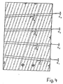
- FIG. 4 shows a phase-shifted DFB grid field which is tilted relative to the left grid boundary by the angle between a grid line and the preferred direction ⁇ . The meaning of the adjustment crosses is explained in FIGS. 7 and 8 using an example.
- Another advantage of the arrangement shown in FIG. 4 ( ⁇ > 0) over the examples shown in FIGS. 2 and 3 is that the entry or exit angles of the optical waveguide i, ⁇ i can be chosen to be significantly smaller if a specific wavelength shift is specified from waveguide to waveguide.
- a possible disadvantage of this example is the local shift of the location of the phase shift in the x direction from waveguide to waveguide.
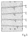
- FIG. 5 shows a DFB grating that is not out of phase, which is opposite the left grid boundary by the angle between a grid line and the preferred direction ⁇ is tilted.
- the angle and shown Waveguide configuration corresponds to that in FIG. 4 shown waveguide configuration. Since the Phase shift in all 4 waveguides shown through a defined partial length of the waveguide reduced width is realized (local, section by section Waveguide constriction), is the location of the phase shift Precisely adjustable in the x direction.
- the disadvantage of having the solution described in Figure 4 can be connected as shown in Figure 5 are bypassed.
- FIG. 6 shows a phase-shifted DFB grid field which is tilted by the angle ⁇ with respect to the left grid boundary.
- the alignment marks are indicated, which are contained in Figures 2-6.
- the following 2 pictures explain an example for the use of the alignment marks.
- the adjustment crosses can be omitted with identical, precisely controllable reference of all process steps to a preferred direction of the component.
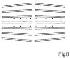
- FIG. 7 shows the example of a DFB grating written with electron beam lithography, including the defined alignment crosses, which are aligned relative to a defined preferred direction, as shown in Examples 4-6. This procedure defines the angle between a grid line and the preferred direction ⁇ .
- a mask as shown in FIG. 8 can be used, which also contains suitable complementary marking crosses (alignment marks) which, when the corresponding crosses are correctly aligned one above the other, define the entry or exit angles ⁇ i of the optical waveguide i and the angles ⁇ i .
- FIGS. 7 and 8 are superimposed, an adjustment is obtained after adjusting the corresponding crosses, which is similar in sections to the arrangement according to FIG. 6.
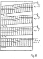
- FIG. 9 shows a partial view of a component with 4 Waveguides.
- Another advantage of this solution is that the phase shift integrated in the grid Place in the x direction in the waveguide can. In this example, too, the individual Grid fields with the cheaper holographic Realize method.
- Each grid field i can strip-shaped, as shown in Figure 9, where previously the angle ⁇ between a grid line and the preferred direction directly by turning the Semiconductor wafers was set.
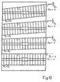
- Figure 10 shows the solution corresponding to Figure 9, at which is the phase shift in each waveguide by a local, section-wise enlargement of the waveguide width is defined.
- FIG. 11 shows the one corresponding to FIGS. 9 and 10 Solution where the phase shift in each Waveguide through a section-wise curvature of the Waveguide is defined.
- This solution allows one efficient spatial distribution of the phase shift.
- the Solutions which are shown in Figures 9-11, guarantee equal lengths of all waveguides if the left and right grid boundaries parallel to each other be chosen, such as B. in crystallographic Columns.
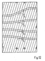
- FIG. 12 shows a DFB grating that is not out of phase, which is opposite the left grid boundary by the angle between a grid line and the preferred direction ⁇ is tilted.
- the phase shift is in each Waveguide through an individual waveguide curvature realized.
- everyone is Three straight and two curved waveguides Sections built.
- FIG. 13 shows a non-phase-shifted DFB grating, which is opposite the left grid boundary by the angle ⁇ is tilted.
- the phase shift is in each Waveguide through an individual waveguide solution realized and is here over the entire length of the grid distributed.
- FIG. 14 shows a non-phase-shifted DFB grating, which is opposite the left grid boundary by the angle between a grid line and the preferred direction ⁇ is tilted.
- the phase shift is in each Waveguide through an individual waveguide curvature realized.
- everyone is Three straight and four curved waveguides Sections built.
- ⁇ i, i + 1 and ⁇ i, i + 1 is the angle difference between adjacent waveguides.
- ⁇ 12 is unusually large. This disadvantage is avoided in the following examples.
- This example also corresponds to FIGS. 2 and 3.
- the angle differences ⁇ i, i + 1 are significantly reduced.
- This example also corresponds to FIGS. 2 and 3 and shows that even large wavelength differences ⁇ i, i + 1 can be realized.
Landscapes
- Physics & Mathematics (AREA)
- General Physics & Mathematics (AREA)
- Optics & Photonics (AREA)
- Condensed Matter Physics & Semiconductors (AREA)
- Electromagnetism (AREA)
- Engineering & Computer Science (AREA)
- Microelectronics & Electronic Packaging (AREA)
- Optical Integrated Circuits (AREA)
- Luminescent Compositions (AREA)
Claims (32)
- Composant optoélectronique à longueurs d'onde multiples, composé de n guides d'ondes optiques, dont les axes optiques sont disposés l'un à côté de l'autre sur le plan xy, chaque guide d'ondes ayant sur toute sa longueur la même largeur ou présentant une variation locale de sa largeur par segment, tel que, dans les parties des guides d'ondes optiques dans lesquelles l'intensité des champs lumineux diffusés s'écarte nettement de zéro, se trouve une grille optique de rétroaction, laquelle soit ne présente pas de décalage de phase et est caractérisée par une période constante de corrugation, soit présente un ou plusieurs décalages de phase et a généré une période constante de corrugation en dehors des décalages de phase, les angles ϑi entre les perpendiculaires aux lignes de la grille et la direction des guides d'ondes lumineuses sur le plan xy étant compris entre - 50° et + 50°, au moins deux guides d'ondes optiques à angles ϑi différents étant placés sur le composant, la période effective de corrugation de guide d'ondes à guide d'ondes étant modifiée de manière ciblée par la mesure individuelle de l'angle ϑi pour chaque guide d'ondes et l'angle ϑi nécessaire pour la longueur d'onde de Bragg du guide d'ondes λB,i pour une grille de premier ordre étant calculé pour chaque guide d'ondes selon la formule
caractérisé en ce que les lignes de la grille de rétroaction placées dans le composant optoélectronique sont inclinées par rapport à une direction préférentielle définie selon des critères cristallographiques ou ayant trait à la géométrie du composant, de l'angle ϕ, ϕ > 0, entre une ligne de la grille et la direction préférentielle du guide d'ondes i. - Composant optoélectronique à longueurs d'onde multiples selon la revendication 1, caractérisé en ce qu'il existe en plus dans les directions des guides d'ondes un nombre défini de domaines hors grille, de sorte qu'il en résulte une structure DBR.
- Composant optoélectronique à longueurs d'onde multiples selon la revendication 1, caractérisé en ce qu'il existe en plus dans les directions des guides d'ondes un nombre défini de domaines hors grille spéciaux, de sorte qu'il en résulte une structure de « sampled grating ».
- Composant optoélectronique à longueurs d'onde multiples selon la revendication 1, caractérisé en ce qu'il existe, entre deux plans parallèles au plan xy, plusieurs champs de grille différemment inclinés par rapport à une direction préférentielle, un guide d'ondes étant affecté à chaque champ de grille.
- Composant optoélectronique à longueurs d'onde multiples selon la revendication 1, caractérisé en ce qu'il existe, entre deux plans parallèles au plan xy, plusieurs champs de grille différemment inclinés par rapport à une direction préférentielle, plusieurs guides d'ondes étant affectés à chaque champ de grille.
- Composant optoélectronique à longueurs d'onde multiples selon la revendication 1, caractérisé en ce que l'un des guides d'ondes coupe perpendiculairement les lignes de la grille.
- Composant optoélectronique à longueurs d'onde multiples selon la revendication 1, caractérisé en ce qu'aucun des guides d'ondes ne coupe perpendiculairement les lignes de la grille
- Composant optoélectronique à longueurs d'onde multiples selon la revendication 1, caractérisé en ce que plusieurs guides d'ondes coupent perpendiculairement les lignes de la grille.
- Composant optoélectronique à longueurs d'onde multiples selon la revendication 1, caractérisé en ce que tous les guides d'ondes optiques i forment des angles ϑi différents avec les lignes de la grille.
- Composant optoélectronique à longueurs d'onde multiples selon la revendication 1, caractérisé en ce que plusieurs des n guides d'ondes optiques sont disposés selon le même angle ϑi.
- Composant optoélectronique à longueurs d'onde multiples selon la revendication 1, caractérisé en ce que l'angle ϑi augmente dans une séquence de guides d'ondes i = 1, 2, 3,...n.
- Composant optoélectronique à longueurs d'onde multiples selon la revendication 1, caractérisé en ce que l'angle ϑi diminue dans une séquence de guides d'ondes i = 1, 2, 3,... n.
- Composant optoélectronique à longueurs d'onde multiples selon la revendication 1, caractérisé en ce que l'affectation des angles ϑi aux différents guides d'ondes est indifférente.
- Composant optoélectronique à longueurs d'onde multiples selon la revendication 1, caractérisé en ce que les lignes de chaque champ de grille i correspondant à un guide d'ondes i sont inclinées d'un angle individuel ϕi par rapport à une direction préférentielle.
- Composant optoélectronique à longueurs d'onde multiples selon la revendication 1, caractérisé en ce que les lignes de chaque champ de grille i correspondant à un guide d'ondes i sont inclinées d'un angle individuel ϕi par rapport à une direction préférentielle, les guides d'ondes étant définis comme perpendiculaires par rapport aux facettes de clivage.
- Composant optoélectronique à longueurs d'onde multiples selon la revendication 1, caractérisé en ce que les lignes de chaque champ de grille i correspondant à un guide d'ondes i sont inclinées d'un angle individuel ϕi par rapport à une direction préférentielle, l'angle d'entrée ou de sortie αi, l'angle ϑi et l'angle ϕi entre une ligne de la grille et la direction préférentielle étant totalement indépendants les uns des autres.
- Composant optoélectronique à longueurs d'onde multiples selon la revendication 1, caractérisé en ce que le décalage de phase est généré dans les grilles, de sorte qu'un décalage de phase a lieu à l'intérieur d'un guide d'ondes.
- Composant optoélectronique à longueurs d'onde multiples selon la revendication 1, caractérisé en ce qu'il y a décalage de phase à l'intérieur de la grille, le décalage de phase total à l'intérieur d'un guide d'ondes étant subdivisé dans la grille en plusieurs décalages de phase répartis sur la longueur du guide d'ondes.
- Composant optoélectronique à longueurs d'onde multiples selon la revendication 1, caractérisé en ce que, pour chaque guide d'ondes, un décalage de phase est réalisé par une modification ciblée, locale et par segment de la largeur du guide d'ondes.
- Composant optoélectronique à longueurs d'onde multiples selon la revendication 1, caractérisé en ce que le décalage de phase total à l'intérieur d'un guide d'ondes est subdivisé en plusieurs décalages de phase répartis sur la direction de diffusion de la lumière, ces différents décalages de phase étant réalisés par des modifications locales par segment de la largeur du guide d'ondes.
- Composant optoélectronique à longueurs d'onde multiples selon la revendication 1, caractérisé en ce que les guides d'ondes i ont différentes largeurs de base di.
- Composant optoélectronique à longueurs d'onde multiples selon la revendication 1, caractérisé en ce qu'il existe, à l'intérieur d'un guide d'ondes, des combinaisons de rétrécissements et d'élargissements du guide d'ondes.
- Composant optoélectronique à longueurs d'onde multiples selon la revendication 1, caractérisé en ce que la jonction sur la grille est complexe et comprend aussi bien une jonction au niveau de l'indice de réfraction qu'au niveau du gain.
- Composant optoélectronique à longueurs d'onde multiples selon la revendication 1, caractérisé en ce que la jonction sur la grille est complexe et comprend aussi bien une jonction au niveau de l'indice de réfraction qu'au niveau de la perte.
- Composant optoélectronique à longueurs d'onde multiples selon la revendication 1, caractérisé en ce que la jonction sur la grille est purement imaginaire et comprend une jonction au niveau du gain.
- Composant optoélectronique à longueurs d'onde multiples selon la revendication 1, caractérisé en ce que la jonction sur la grille est purement imaginaire et comprend une jonction au niveau de la perte.
- Composant optoélectronique à longueurs d'onde multiples selon la revendication 1, caractérisé en ce que la jonction sur la grille est réelle et purement au niveau de l'indice.
- Composant optoélectronique à longueurs d'onde multiples selon la revendication 1, caractérisé en ce que les guides d'ondes sont plus ou moins courbés.
- Composant optoélectronique à longueurs d'onde multiples selon la revendication 1, caractérisé en ce que le décalage de phase total à l'intérieur de chaque guide d'ondes est défini par une fonction de courbure du guide d'ondes individuellement ciblée.
- Composant optoélectronique à longueurs d'onde multiples selon la revendication 1, caractérisé en ce que chaque guide d'ondes est constitué d'une combinaison quelconque de tronçons droits et individuellement courbés.
- Composant optoélectronique à longueurs d'onde multiples selon la revendication 1, caractérisé en ce que le décalage de phase total à l'intérieur de chaque guide d'ondes est défini par une combinaison de variation locale de la largeur du guide d'ondes, de décalages de phase dans la grille et d'une courbure du guide d'ondes.
- Composant optoélectronique à longueurs d'onde multiples selon la revendication 1, caractérisé en ce que les angles ϑi et les angles αi d'entrée ou de sortie du guide d'ondes sont inférieurs à 50°.
Applications Claiming Priority (2)
| Application Number | Priority Date | Filing Date | Title |
|---|---|---|---|
| DE4432410A DE4432410B4 (de) | 1994-08-31 | 1994-08-31 | Optoelektronisches Multi-Wellenlängen-Bauelement |
| DE4432410 | 1994-08-31 |
Publications (2)
| Publication Number | Publication Date |
|---|---|
| EP0704946A1 EP0704946A1 (fr) | 1996-04-03 |
| EP0704946B1 true EP0704946B1 (fr) | 2003-10-01 |
Family
ID=6527999
Family Applications (1)
| Application Number | Title | Priority Date | Filing Date |
|---|---|---|---|
| EP95110326A Expired - Lifetime EP0704946B1 (fr) | 1994-08-31 | 1995-07-03 | Composant opto-électronique multi-longueurs d'onde |
Country Status (4)
| Country | Link |
|---|---|
| US (1) | US5600743A (fr) |
| EP (1) | EP0704946B1 (fr) |
| AT (1) | ATE251353T1 (fr) |
| DE (2) | DE4432410B4 (fr) |
Families Citing this family (14)
| Publication number | Priority date | Publication date | Assignee | Title |
|---|---|---|---|---|
| KR100263195B1 (ko) * | 1996-09-16 | 2000-08-01 | 윤종용 | 광도파로 소자의 제작 방법 |
| DE19708385A1 (de) * | 1997-03-01 | 1998-09-03 | Deutsche Telekom Ag | Wellenlängenabstimmbares optoelektronisches Bauelement |
| FR2766582A1 (fr) | 1997-07-23 | 1999-01-29 | Corning Inc | Methode de fabrication de composant optique et composant optique fabrique selon cette methode |
| US6242137B1 (en) * | 1999-09-21 | 2001-06-05 | Promos Technology, Inc | Method to uni-directionally expand bandwidth of an asymmetric optical system |
| DE10047681A1 (de) * | 2000-09-25 | 2002-04-25 | Aifotec Gmbh | Verfahren zur Herstellung eines Lichtwellenleiter-Arrays mit periodischen Brechungsindex-Modulationen der einzelnen Lichtwellenleiter |
| US20030017421A1 (en) * | 2001-07-18 | 2003-01-23 | Miri Park | Holographic grating fabrication using mirror with surface curvature |
| US6816648B2 (en) * | 2002-05-01 | 2004-11-09 | Intel Corporation | Integrated waveguide gratings by ion implantation |
| EP1391756A1 (fr) * | 2002-08-20 | 2004-02-25 | Agilent Technologies, Inc. - a Delaware corporation - | Dispositif à réflecteur de Bragg distribué sélectif en longueur d'onde |
| JP4629022B2 (ja) | 2005-12-27 | 2011-02-09 | 住友電工デバイス・イノベーション株式会社 | レーザ装置、レーザモジュール、および、半導体レーザ |
| DE102014207723A1 (de) * | 2014-04-24 | 2015-10-29 | Fraunhofer-Gesellschaft zur Förderung der angewandten Forschung e.V. | Laser mit verteilter Rückkopplung |
| CN108233177B (zh) * | 2018-01-22 | 2019-06-18 | 华中科技大学 | 一种可调谐半导体激光器 |
| US11398715B2 (en) * | 2018-02-26 | 2022-07-26 | Panasonic Holdings Corporation | Semiconductor light emitting device |
| CN115764542A (zh) * | 2021-09-02 | 2023-03-07 | 中兴光电子技术有限公司 | 双波长半导体激光器及其制备方法 |
| US20250013041A1 (en) * | 2023-07-05 | 2025-01-09 | Applied Materials, Inc. | Projector compensation with incoupler grating line offset |
Family Cites Families (37)
| Publication number | Priority date | Publication date | Assignee | Title |
|---|---|---|---|---|
| US3814498A (en) * | 1972-05-04 | 1974-06-04 | Bell Telephone Labor Inc | Integrated optical circuit devices employing optical gratings |
| FR2417866A1 (fr) * | 1978-02-17 | 1979-09-14 | Thomson Csf | Laser multiple a resonateur distribue |
| FR2424674A1 (fr) * | 1978-04-25 | 1979-11-23 | Thomson Csf | Circuit optique integre de demultiplexage |
| US4241109A (en) * | 1979-04-30 | 1980-12-23 | Bell Telephone Laboratories, Incorporated | Technique for altering the profile of grating relief patterns |
| JPS5848981A (ja) * | 1981-09-18 | 1983-03-23 | Agency Of Ind Science & Technol | 半導体レ−ザ装置 |
| JPS5878487A (ja) * | 1981-10-29 | 1983-05-12 | Kokusai Denshin Denwa Co Ltd <Kdd> | 分布帰還形半導体レ−ザ |
| NL8304311A (nl) * | 1983-12-15 | 1985-07-01 | Philips Nv | Reflectieraster. |
| JPS60242686A (ja) * | 1984-05-17 | 1985-12-02 | Nec Corp | 半導体レ−ザアレイ |
| US4660208A (en) * | 1984-06-15 | 1987-04-21 | American Telephone And Telegraph Company, At&T Bell Laboratories | Semiconductor devices employing Fe-doped MOCVD InP-based layer for current confinement |
| US4888624A (en) * | 1984-06-15 | 1989-12-19 | American Telephone And Telegraph Company, At&T Bell Laboratories | Semiconductor devices employing high resistivity in-based compound group III-IV epitaxial layer for current confinement |
| US4595454A (en) * | 1984-06-15 | 1986-06-17 | At&T Bell Laboratories | Fabrication of grooved semiconductor devices |
| US4999315A (en) * | 1984-06-15 | 1991-03-12 | At&T Bell Laboratories | Method of controlling dopant incorporation in high resistivity In-based compound Group III-V epitaxial layers |
| JPS6189690A (ja) * | 1984-10-09 | 1986-05-07 | Fujitsu Ltd | 半導体レ−ザ |
| US4733927A (en) * | 1984-11-14 | 1988-03-29 | Hughes Aircraft Company | Stress waveguides in bulk crystalline materials |
| GB2169134B (en) * | 1984-11-16 | 1988-11-16 | Canon Kk | Multibeam emitting device |
| JPS62124791A (ja) * | 1985-11-25 | 1987-06-06 | Matsushita Electric Ind Co Ltd | 半導体レ−ザ |
| JPS62144378A (ja) * | 1985-12-18 | 1987-06-27 | Sony Corp | 分布帰還覆半導体レ−ザ− |
| JPS62158377A (ja) * | 1985-12-28 | 1987-07-14 | Sony Corp | 分布帰還型半導体レ−ザ− |
| US4902644A (en) * | 1986-03-28 | 1990-02-20 | American Telephone And Telegraph Company At&T Bell Laboratories | Preservation of surface features on semiconductor surfaces |
| US4805178A (en) * | 1986-03-28 | 1989-02-14 | American Telephone And Telegraph Company, At&T Bell Laboratories | Preservation of surface features on semiconductor surfaces |
| US5058977A (en) * | 1987-01-20 | 1991-10-22 | Hewlett-Packard Company | Broadband tunable in-line filter for fiber optics |
| US4815084A (en) * | 1987-05-20 | 1989-03-21 | Spectra Diode Laboratories, Inc. | Semiconductor laser with integrated optical elements |
| US4867515A (en) * | 1988-08-05 | 1989-09-19 | Canadian Patents And Development Ltd. | All-optical modulator with a channel waveguide |
| US4941725A (en) * | 1988-08-05 | 1990-07-17 | Canadian Patents & Development Limited | All-optical planar modulator structure with channel waveguides |
| DE4001726A1 (de) * | 1990-01-22 | 1991-07-25 | Siemens Ag | Verfahren zur herstellung von dfb-gittern mit um eine halbe gitterkonstante gegeneinander versetzten anteilen |
| DE69128786T2 (de) * | 1990-06-06 | 1998-08-20 | Kol Ohr Corp., Wilmington, Del. | Abstimmbare Lichtquelle und faseroptische Systeme mit abstimmbarer Lichtquelle |
| JPH04221873A (ja) * | 1990-12-21 | 1992-08-12 | Nippon Telegr & Teleph Corp <Ntt> | 半導体集積化光源 |
| JP2907234B2 (ja) * | 1990-12-21 | 1999-06-21 | 日本電信電話株式会社 | 半導体波長可変装置 |
| US5185754A (en) * | 1991-07-29 | 1993-02-09 | Spectra Diode Laboratories, Inc. | Spectrally stable laser diode with internal reflector |
| US5231642A (en) * | 1992-05-08 | 1993-07-27 | Spectra Diode Laboratories, Inc. | Semiconductor ring and folded cavity lasers |
| SE470454B (sv) * | 1992-08-26 | 1994-04-11 | Ericsson Telefon Ab L M | Optisk filteranordning |
| US5384797A (en) * | 1992-09-21 | 1995-01-24 | Sdl, Inc. | Monolithic multi-wavelength laser diode array |
| DE4233500A1 (de) * | 1992-10-06 | 1994-04-07 | Ant Nachrichtentech | Lichtwellenleiter zur kontinuierlichen Phasenverschiebung der DFB-Gitterperiode für auf DFB-Gitterfeldern mit konstanter Gitterperiode basierende optoelektronische Komponenten |
| US5327515A (en) * | 1993-01-14 | 1994-07-05 | At&T Laboratories | Method for forming a Bragg grating in an optical medium |
| DE4322163A1 (de) * | 1993-07-03 | 1995-01-12 | Ant Nachrichtentech | Auf DFB- oder DBR-Gitter basierendes optoelektronisches Bauelement mit quasi-kontinuierlich axial verteilbarer Brechungsindex-Variation, mit axial beliebig verteilbarer und variierbarer Phasenverschiebung, sowie mit axial quasi-kontinuierlich variierbarem Gitter-Kopplungskoeffizienten |
| DE4322164A1 (de) * | 1993-07-03 | 1995-01-12 | Ant Nachrichtentech | Optoelektronisches Bauelement mit Rückkopplungsgitter, mit axial quasi-kontinuierlich und nahezu beliebig variierbarem Gitterkopplungs-Koeffizienten, mit quasi-kontinuierlich axial verteilbarer Brechungsindex-Variation, sowie mit axial nahezu beliebig verteilbarer und variierbarer Phasenverschiebung |
| EP0641053A1 (fr) * | 1993-08-30 | 1995-03-01 | AT&T Corp. | Méthode et dispositif de contrôle de la longeur d'onde dans des lasers du type DFB |
-
1994
- 1994-08-31 DE DE4432410A patent/DE4432410B4/de not_active Expired - Fee Related
-
1995
- 1995-07-03 AT AT95110326T patent/ATE251353T1/de active
- 1995-07-03 EP EP95110326A patent/EP0704946B1/fr not_active Expired - Lifetime
- 1995-07-03 DE DE59510800T patent/DE59510800D1/de not_active Expired - Fee Related
- 1995-08-28 US US08/520,070 patent/US5600743A/en not_active Expired - Lifetime
Non-Patent Citations (1)
| Title |
|---|
| KADEN C. ET AL: "Fabrication of nonconventional distributed feedback lasers with variable grating periods and phase shifts by electron beam lithography", JOURNAL OF VACUUM SCIENCE & TECHNOLOGY, vol. 10, no. 6, 1 November 1992 (1992-11-01), NEW YORK, USA, pages 2970 - 2973, XP000332508 * |
Also Published As
| Publication number | Publication date |
|---|---|
| DE59510800D1 (de) | 2003-11-06 |
| DE4432410B4 (de) | 2007-06-21 |
| EP0704946A1 (fr) | 1996-04-03 |
| DE4432410A1 (de) | 1996-03-07 |
| ATE251353T1 (de) | 2003-10-15 |
| US5600743A (en) | 1997-02-04 |
Similar Documents
| Publication | Publication Date | Title |
|---|---|---|
| EP0885402B1 (fr) | Filtre de separation optique a voies multiples avec cristaux photoniques electriquement ajustables | |
| EP0418705B1 (fr) | Laser à semi-conducteur interférométrique | |
| DE69733670T2 (de) | Optischer demultiplexer mit einem beugungsgitter | |
| EP0704946B1 (fr) | Composant opto-électronique multi-longueurs d'onde | |
| DE60318762T2 (de) | Faser-zu-Wellenleiter-Koppler mit Beugungsgitter für polarisationserhaltende optische integrierte Schaltungen | |
| DE69329358T2 (de) | Vorrichtung und Verfahren zur Verstärkung optischer Energie durch Zweistrahl-Kopplung | |
| DE69607493T2 (de) | Polarisationsmodenselektiver Halbleiterlaser, Modulationsverfahren und optisches Kommunikationssystem unter Verwendung dieses Lasers | |
| DE69507486T2 (de) | Faseroptischer hochleistungsverstaerker oder laservorrichtung | |
| DE69120479T2 (de) | Durch elektrisches feld induzierter quanten-potentialtopf-wellenleiter | |
| DE19948353B4 (de) | Laserstrahlungsquelle und Verfahren zum Erzeugen eines kohärenten Gesamtlaserstrahlungsfeldes | |
| EP2478400A2 (fr) | Filtres de modes transversaux pour guide d'onde | |
| DE69225356T2 (de) | Optische Vorrichtung mit einem optischen Koppler zum Verzweigen/Kombinieren und einem optischen Verstärker und dazugehörige Methode zum Verzweigen/Kombinieren | |
| DE4407832A1 (de) | Verfahren zur Herstellung eines optoelektronischen Bauelements mit einer definierten axialen Variation des Kopplungskoeffizienten und definierter axialer Verteilung der Phasenverschiebung | |
| EP1295371B1 (fr) | Resonateurs laser a structures de phases a selection de mode | |
| WO1999052003A1 (fr) | Configuration destinee a la separation et/ou la reunion spatiale de canaux de longueurs d'ondes optiques | |
| DE102020108941B4 (de) | Diodenlaser mit verrringerter Strahldivergenz | |
| DE19626130A1 (de) | Optisches Halbleiterbauelement mit tiefem Rippenwellenleiter | |
| DE3875768T2 (de) | Halbleiterlaser mit verteilter rueckkopplung. | |
| DE69118563T2 (de) | Laservorrichtung | |
| DE10160502B4 (de) | Optische Mikrowellenquelle | |
| DE69012528T2 (de) | Vorrichtung zur kontinuierlichen Abstimmung einer kohärenten und linear polarisierten Lichtquelle. | |
| DE3889423T2 (de) | Filter mit abstimmbarer Wellenlänge. | |
| EP0216212A2 (fr) | Résonateur optique extérieur pour un laser à semi-conducteur | |
| DE69511097T2 (de) | Optischer multiwellenlaengen-wellenleiterfilter | |
| DE4423187A1 (de) | Abstimmbare optische Anordnung |
Legal Events
| Date | Code | Title | Description |
|---|---|---|---|
| PUAI | Public reference made under article 153(3) epc to a published international application that has entered the european phase |
Free format text: ORIGINAL CODE: 0009012 |
|
| AK | Designated contracting states |
Kind code of ref document: A1 Designated state(s): AT BE CH DE DK ES FR GB GR IE IT LI LU MC NL PT SE |
|
| 17P | Request for examination filed |
Effective date: 19960625 |
|
| 17Q | First examination report despatched |
Effective date: 19980318 |
|
| RAP1 | Party data changed (applicant data changed or rights of an application transferred) |
Owner name: DEUTSCHE TELEKOM AG |
|
| RIC1 | Information provided on ipc code assigned before grant |
Free format text: 7H 01S 5/10 A, 7G 02B 6/12 B |
|
| RTI1 | Title (correction) |
Free format text: OPTOELECTRONIC MULTIWAVELENGTH ELEMENT |
|
| GRAH | Despatch of communication of intention to grant a patent |
Free format text: ORIGINAL CODE: EPIDOS IGRA |
|
| RIC1 | Information provided on ipc code assigned before grant |
Ipc: 7G 02B 6/12 B Ipc: 7H 01S 5/10 A |
|
| RTI1 | Title (correction) |
Free format text: OPTOELECTRONIC MULTIWAVELENGTH ELEMENT |
|
| GRAS | Grant fee paid |
Free format text: ORIGINAL CODE: EPIDOSNIGR3 |
|
| GRAA | (expected) grant |
Free format text: ORIGINAL CODE: 0009210 |
|
| AK | Designated contracting states |
Kind code of ref document: B1 Designated state(s): AT BE CH DE DK ES FR GB GR IE IT LI LU MC NL PT SE |
|
| PG25 | Lapsed in a contracting state [announced via postgrant information from national office to epo] |
Ref country code: NL Free format text: LAPSE BECAUSE OF FAILURE TO SUBMIT A TRANSLATION OF THE DESCRIPTION OR TO PAY THE FEE WITHIN THE PRESCRIBED TIME-LIMIT Effective date: 20031001 Ref country code: IE Free format text: LAPSE BECAUSE OF FAILURE TO SUBMIT A TRANSLATION OF THE DESCRIPTION OR TO PAY THE FEE WITHIN THE PRESCRIBED TIME-LIMIT Effective date: 20031001 |
|
| REG | Reference to a national code |
Ref country code: GB Ref legal event code: FG4D Free format text: NOT ENGLISH |
|
| REG | Reference to a national code |
Ref country code: CH Ref legal event code: EP |
|
| REG | Reference to a national code |
Ref country code: IE Ref legal event code: FG4D Free format text: GERMAN |
|
| REF | Corresponds to: |
Ref document number: 59510800 Country of ref document: DE Date of ref document: 20031106 Kind code of ref document: P |
|
| PG25 | Lapsed in a contracting state [announced via postgrant information from national office to epo] |
Ref country code: GR Free format text: LAPSE BECAUSE OF FAILURE TO SUBMIT A TRANSLATION OF THE DESCRIPTION OR TO PAY THE FEE WITHIN THE PRESCRIBED TIME-LIMIT Effective date: 20040101 Ref country code: DK Free format text: LAPSE BECAUSE OF FAILURE TO SUBMIT A TRANSLATION OF THE DESCRIPTION OR TO PAY THE FEE WITHIN THE PRESCRIBED TIME-LIMIT Effective date: 20040101 |
|
| PG25 | Lapsed in a contracting state [announced via postgrant information from national office to epo] |
Ref country code: ES Free format text: LAPSE BECAUSE OF FAILURE TO SUBMIT A TRANSLATION OF THE DESCRIPTION OR TO PAY THE FEE WITHIN THE PRESCRIBED TIME-LIMIT Effective date: 20040112 |
|
| REG | Reference to a national code |
Ref country code: SE Ref legal event code: TRGR |
|
| GBT | Gb: translation of ep patent filed (gb section 77(6)(a)/1977) |
Effective date: 20040115 |
|
| NLV1 | Nl: lapsed or annulled due to failure to fulfill the requirements of art. 29p and 29m of the patents act | ||
| REG | Reference to a national code |
Ref country code: IE Ref legal event code: FD4D |
|
| PG25 | Lapsed in a contracting state [announced via postgrant information from national office to epo] |
Ref country code: LU Free format text: LAPSE BECAUSE OF NON-PAYMENT OF DUE FEES Effective date: 20040703 |
|
| ET | Fr: translation filed | ||
| PG25 | Lapsed in a contracting state [announced via postgrant information from national office to epo] |
Ref country code: MC Free format text: LAPSE BECAUSE OF NON-PAYMENT OF DUE FEES Effective date: 20040731 Ref country code: LI Free format text: LAPSE BECAUSE OF NON-PAYMENT OF DUE FEES Effective date: 20040731 Ref country code: CH Free format text: LAPSE BECAUSE OF NON-PAYMENT OF DUE FEES Effective date: 20040731 Ref country code: BE Free format text: LAPSE BECAUSE OF NON-PAYMENT OF DUE FEES Effective date: 20040731 |
|
| PLBE | No opposition filed within time limit |
Free format text: ORIGINAL CODE: 0009261 |
|
| STAA | Information on the status of an ep patent application or granted ep patent |
Free format text: STATUS: NO OPPOSITION FILED WITHIN TIME LIMIT |
|
| 26N | No opposition filed |
Effective date: 20040702 |
|
| BERE | Be: lapsed |
Owner name: DEUTSCHE *TELEKOM A.G. Effective date: 20040731 |
|
| PG25 | Lapsed in a contracting state [announced via postgrant information from national office to epo] |
Ref country code: DE Free format text: LAPSE BECAUSE OF NON-PAYMENT OF DUE FEES Effective date: 20050201 |
|
| REG | Reference to a national code |
Ref country code: CH Ref legal event code: PL |
|
| BERE | Be: lapsed |
Owner name: DEUTSCHE *TELEKOM A.G. Effective date: 20040731 |
|
| PG25 | Lapsed in a contracting state [announced via postgrant information from national office to epo] |
Ref country code: PT Free format text: LAPSE BECAUSE OF NON-PAYMENT OF DUE FEES Effective date: 20040301 |
|
| PGFP | Annual fee paid to national office [announced via postgrant information from national office to epo] |
Ref country code: FR Payment date: 20110805 Year of fee payment: 17 |
|
| PGFP | Annual fee paid to national office [announced via postgrant information from national office to epo] |
Ref country code: GB Payment date: 20110725 Year of fee payment: 17 Ref country code: SE Payment date: 20110727 Year of fee payment: 17 Ref country code: AT Payment date: 20110621 Year of fee payment: 17 |
|
| PGFP | Annual fee paid to national office [announced via postgrant information from national office to epo] |
Ref country code: IT Payment date: 20110727 Year of fee payment: 17 |
|
| REG | Reference to a national code |
Ref country code: SE Ref legal event code: EUG |
|
| REG | Reference to a national code |
Ref country code: AT Ref legal event code: MM01 Ref document number: 251353 Country of ref document: AT Kind code of ref document: T Effective date: 20120703 |
|
| GBPC | Gb: european patent ceased through non-payment of renewal fee |
Effective date: 20120703 |
|
| REG | Reference to a national code |
Ref country code: FR Ref legal event code: ST Effective date: 20130329 |
|
| PG25 | Lapsed in a contracting state [announced via postgrant information from national office to epo] |
Ref country code: GB Free format text: LAPSE BECAUSE OF NON-PAYMENT OF DUE FEES Effective date: 20120703 Ref country code: SE Free format text: LAPSE BECAUSE OF NON-PAYMENT OF DUE FEES Effective date: 20120704 Ref country code: FR Free format text: LAPSE BECAUSE OF NON-PAYMENT OF DUE FEES Effective date: 20120731 |
|
| PG25 | Lapsed in a contracting state [announced via postgrant information from national office to epo] |
Ref country code: IT Free format text: LAPSE BECAUSE OF NON-PAYMENT OF DUE FEES Effective date: 20120703 |
|
| PG25 | Lapsed in a contracting state [announced via postgrant information from national office to epo] |
Ref country code: AT Free format text: LAPSE BECAUSE OF NON-PAYMENT OF DUE FEES Effective date: 20120703 |