EP0704973A2 - Vorrichtung und Verfahren zum Schutz einer elektrischen Schaltung - Google Patents
Vorrichtung und Verfahren zum Schutz einer elektrischen Schaltung Download PDFInfo
- Publication number
- EP0704973A2 EP0704973A2 EP95306702A EP95306702A EP0704973A2 EP 0704973 A2 EP0704973 A2 EP 0704973A2 EP 95306702 A EP95306702 A EP 95306702A EP 95306702 A EP95306702 A EP 95306702A EP 0704973 A2 EP0704973 A2 EP 0704973A2
- Authority
- EP
- European Patent Office
- Prior art keywords
- pad
- circuit
- volt
- pux
- pdx
- Prior art date
- Legal status (The legal status is an assumption and is not a legal conclusion. Google has not performed a legal analysis and makes no representation as to the accuracy of the status listed.)
- Granted
Links
- 238000000034 method Methods 0.000 title claims description 12
- 230000006378 damage Effects 0.000 claims abstract description 20
- 239000004065 semiconductor Substances 0.000 claims description 5
- 239000004020 conductor Substances 0.000 description 63
- 239000000758 substrate Substances 0.000 description 29
- 230000001681 protective effect Effects 0.000 description 7
- 239000000463 material Substances 0.000 description 5
- 230000001052 transient effect Effects 0.000 description 4
- 230000005540 biological transmission Effects 0.000 description 3
- 238000010586 diagram Methods 0.000 description 3
- 238000004519 manufacturing process Methods 0.000 description 3
- 238000005516 engineering process Methods 0.000 description 2
- 230000002459 sustained effect Effects 0.000 description 2
- 230000003139 buffering effect Effects 0.000 description 1
- 230000015556 catabolic process Effects 0.000 description 1
- 230000002301 combined effect Effects 0.000 description 1
- 230000005684 electric field Effects 0.000 description 1
Images

Classifications
-
- H—ELECTRICITY
- H03—ELECTRONIC CIRCUITRY
- H03K—PULSE TECHNIQUE
- H03K19/00—Logic circuits, i.e. having at least two inputs acting on one output; Inverting circuits
- H03K19/003—Modifications for increasing the reliability for protection
- H03K19/00315—Modifications for increasing the reliability for protection in field-effect transistor circuits
-
- H—ELECTRICITY
- H10—SEMICONDUCTOR DEVICES; ELECTRIC SOLID-STATE DEVICES NOT OTHERWISE PROVIDED FOR
- H10D—INORGANIC ELECTRIC SEMICONDUCTOR DEVICES
- H10D99/00—Subject matter not provided for in other groups of this subclass
Definitions
- the present invention relates to an electrical circuit protection arrangement and method, and in particular to an arrangement and method useful in integrated circuit devices for buffering and protecting interconnected devices optimized for different voltage sources.
- I/O PADS In integrated circuit technology, devices in different integrated circuit (hereinafter referred to as "IC") packages are interconnected to one another at I/O PADS associated with each IC package.
- I/O PADS are associated with electrical circuits which perform a desired function to interface with other IC packages or electrical devices.
- An I/O PAD may be associated with electrical circuits which generate output signals and apply the signals to the I/O PAD for external devices to sense and process accordingly.
- an I/O PAD may be associated with electrical circuits which sense the logic state of signals applied to the I/O PAD by external electrical circuits or IC packages.
- I/O PADS are frequently "bi-directional" in the sense that they may be used at different times for the sensing of input signals to the IC package or for the application of output signals from the IC package. Electrical output signals are applied to an I/O PAD by electrical circuits within the IC package associated with the I/O PAD. Similarly, electrical input signals are received as input signals from an I/O PAD by associated electrical circuits within the IC package which "sense" the signal level and operate accordingly.
- Transistor gates and other circuits optimized for 3 volt operation may not withstand the application of 5 volt signals to their I/O PADS from other interconnected IC packages.
- the 5 volt signals may breakdown the thinner oxide layers of the 3 volt optimized I/O circuits causing current leakage or even permanent destruction of the oxide layers.
- the present invention seeks to provide for a circuit protection apparatus and method having advantages over known such apparatus and methods.
- an electrical circuit arrangement having pad means and electrical circuits associated with said pad means for exchanging electrical signals via said pad means and with an external electrical device and with circuit protection means for protecting said electrical circuits from damage caused by application of an excess voltage potential to said pad means by said external electrical device characterised in that said circuit protection means comprises first means for applying power to said circuit protection means when said electrical circuits are in a power on state, and second means for applying power to said circuit protection means when said electrical circuits are in a power off state.
- a method of protecting an electrical circuit optimized for operation at a first potential level and having circuit means for handling electrical signals applied to pad means connected to external device means and when receiving a second potential level in excess of said first potential level characterised by the steps of, applying electric potential of about said first potential level to said circuit protection means in response to said circuit means being in a power-on state, deriving an electric potential of about said first potential level from said second potential level applied to said pad means and applying said derived electric potential to said circuit protection means in response to said circuit means being in a power-off state.
- I/O circuitry associated with an I/O PAD of an IC package is optimized for 3 volt operation.
- Additional protective circuitry is supplied by the present invention which protects the 3 volt optimized I/O circuitry from damage due to application of a 5 volt signal to the I/O PAD.
- the protective circuitry of the present invention protects the 3 volt optimized circuitry both when the source voltage of the I/O circuitry is powered on and when powered off.
- the protective circuitry of the present invention operates in a manner similar to well known prior designs when the 3 volt optimized I/O circuitry is powered on. However, when the 3 volt optimized I/O circuits are powered off, the additional protective circuitry of the present invention operates from power supplied by the external 5 volt signal applied to the I/O PAD. In addition, the protective circuitry of the present invention operates in a manner so as to minimize the power dissipated in the IC package due to the power drawn from the external 5 volt signal through the I/O PAD.
- the present invention advantageously protects 3 volt optimized I/O circuitry from damage due to application of an external 5 volt signal to an I/O PAD regardless of whether the 3 volt optimized I/O circuitry is powered on or off.
- I/O related circuits optimized for 3 volt operation and associated with an I/O PAD can be readily protected from damage due to the external application of a 5 volt signal to the I/O PAD.
- Fig. 1 illustrates a typical I/O PAD design well known to one of ordinary skill in the art. Electrical signals from external circuits 1 are applied to I/O PAD 100 via conductor 2. Input receiver signal processing circuits sense the signals applied to I/O PAD 100 via conductor 110 and process the signal appropriately. In other conditions, electrical signals representing a logic level "1" or "0" are applied to I/O PAD 100 via conductor 111 as output signals for transmission to external circuits 1 over conductor 2.
- Pull-up circuitry (PUX) applies a signal to a conductor 112 when a high voltage level signal (V dd ) is to be applied as an output signal on PAD 100 via conductor 111.
- Pull-down circuitry applies a signal to a conductor 113 when a low voltage level signal (V ss ) is to be applied as an output signal on PAD 100 via conductor 111.
- the PUX is normally at an inactive high voltage level (V dd ) and the PDX is normally at an inactive low voltage level (V ss ).
- the gates of p-channel type MOSFET 101 and n-channel MOSFET 102 are both open.
- the source and substrate of p-channel MOSFET 101 are connected to the V dd voltage source.
- the source and substrate of n-channel MOSFET 102 are connected to V ss .
- MOSFET 101 and n-channel MOSFET 102 are connected to conductor 111.
- conductor 111 is "tri-stated" so that an input signal may be applied by external circuits 1 over conductor 2 to I/O PAD 100 and may be sensed by input receiver signal processing circuits.
- the gate of p-channel MOSFET 101 is closed so that conductor 111 is "pulled up" to V dd to thereby apply a high voltage level signal to I/O PAD 100 for transmission to external circuits 1 over the conductor 2.
- the gate of the n-channel MOSFET 102 is closed so that conductor 111 is “pulled down” to V ss to thereby apply a low voltage level signal to I/O PAD 100 for transmission to external circuits 1 over conductor 2.
- I/O PAD 100 When the circuit of Fig. 1 is implemented, as depicted, optimized for V dd at 3 volts (more precisely 3.3 volts), only 3 volt and lower signals may be applied to I/O PAD 100 by external circuits 1 over conductor 2.
- Application of 5 volt electrical signals to I/O PAD 100 may damage the thinner material used in the gate oxide of MOSFETs 101 and 102 (as well as circuitry relating to the input receiver). For example, if a 5 volt signal were applied to I/O PAD 100 by external circuits 1 over conductor 2 while the I/O circuits are powered on and in the "tri-state" condition discussed above, the gate oxide of n-channel MOSFET 102 would have a 5 volt potential across the drain to gate junction. If this potential were sustained for more than a brief transient period, the thin gate oxide layer, optimized for 3 volt operation, could be damaged.
- Fig. 2 illustrates a typical circuit, well known to those of ordinary skill in the art, which allows for tolerance of 5 volt signals being applied to an I/O PAD 200 of a 3 volt optimized design.
- the circuit depicted in Fig. 2 operates in most respects identically to that of Fig. 1. Electrical signals applied by external circuits 1 over conductor 2 to I/O PAD 200 are sensed by input receiver circuitry via conductor 211. However, the electrical signal applied to I/O PAD 200 is first applied to the source of n-channel transistor 204 via conductor 210. The gate of the transistor 204 is connected to V dd (3.3 volts) and its substrate is connected to V ss which thereby limits the voltage passed through to the drain of the transistor to V dd (3.3 volts).
- V dd 3.3 volts
- Transistor 204 protects the input receiver circuitry from potential damage caused by external circuits 1 applying 5 volt electrical signals to I/O PAD 200 over conductor 2.
- One of these three states is applied through conductor 212 onto I/O PAD 200 to drive output signals out to external circuitry 1 over conductor 2 or to permit external circuitry 1 to apply signals to I/O PAD 200 over conductor 2.
- the gate of n-channel transistor 202 is connected to V dd (3.3 volts) and the substrate is connected to V ss which thereby limits any voltage applied to the drain of transistor 203 to V dd (3.3 volts).
- Transistor 202 thereby protects transistor 203 from potential damage to the gate oxide of transistor 203 by external circuits 1 applying 5 volt electrical signals to I/O PAD 200 over conductor 2.
- transistor 201 has its substrate connected to 5 volts to prevent a 5 volt signal applied to I/O PAD 200 from forward biasing the drain-substrate junction of transistor 201 to thereby damage or otherwise interfere with the V dd source voltage supply. If the substrate of transistor 201 were connected to V dd , as in Fig. 1, and a 5 volt signal were applied to I/O PAD 200, then current would flow from I/O PAD 200, through the drain-substrate junction of transistor 201, back to the power source.
- transistors 202 and 204 as depicted in Fig. 2 provides adequate protection of the I/O circuitry while the I/O circuits are powered on. However, if the I/O circuitry is powered off, n-channel transistors 201, 202, and 204 are potentially damaged by external circuits 1 applying a 5 volt signal to I/O PAD 200 over conductor 2. Specifically, n-channel transistors 201, 202, and 204 will each have a 5 volt electric potential across their gate-drain junctions. As described above, this excessive electric field may damage the thin gate oxide layer optimized for 3 volt operation if it is applied for longer than a brief transient period. Such an excessive voltage is referred to herein as an "excess voltage.”
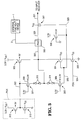
- Fig. 3 illustrates the circuit of the present invention which solves the above problems by providing protection for the I/O circuitry both in power on and power off conditions.
- the circuit of the present invention depicted in Fig. 3 operates in most respects identically to that of FIGS. 1 and 2. Electrical signals applied by external circuits 1 to I/O PAD 300 over conductor 2 are sensed by input receiver circuitry via conductor 321. However, the electrical signal applied to I/O PAD 300 is first applied to the source of n-channel transistor 307 via a conductor 320. The gate of the transistor 307 is connected to conductor 325 and is charged to V dd (3.3 volts) by operation of transistors 302 and 306 as described below. The substrate of transistor 307 is connected to V ss . Transistor 307 protects the input receiver circuitry from potential damage caused by external circuits 1 applying 5 volt electrical signals to I/O PAD 200 over conductor 2.
- One of these three states is applied through conductor 322 onto I/O PAD 300 to drive output signals out to external circuits 1 over conductor 2 or to permit external circuits 1 to apply signals to I/O PAD 300 over conductor 2.
- the gate of n-channel transistor 304 is connected to conductor 325 and is charged to V dd (3.3 volts) by operation of transistors 302 and 306 as described below.
- the substrate of transistor 304 is connected to V ss .
- Transistor 304 limits the voltage applied to the source of transistor 305 to V dd (3.3 volts). Transistor 304 protects transistor 305 from potential damage to the gate oxide of transistor 305 by external circuits 1 applying 5 volt electrical signals to I/O PAD 300 over conductor 2. In addition, transistor 303 has its substrate connected to 5 volts to prevent a 5 volt signal applied to I/O PAD 300 from forward biasing the drain-substrate junction of transistor 303. If the substrate of transistor 303 were connected to V dd , as in Fig. 1, and a 5 volt signal were applied to I/O PAD 300, then current would flow from I/O PAD 300, through the drain-substrate junction of transistor 303, back to the power source.
- p-channel transistor 306 has its gate normally closed to pass through 3 volts (V dd 3.3 volts), connected to its source, to conductor 325, connected to its drain.
- Conductor 325 is connected to the gates of n-channel transistors 307 and 304.
- p-channel transistor 306 applies V dd voltage to the gates of n-channel transistors 307 and 304, thereby closing the gates of transistors 307 and 304 to permit them to protect I/O circuitry in a manner similar to the description above referring to n-channel transistors 204 and 202 of Fig. 2, respectively.
- the protection circuits of Fig.3 provide further protection of the I/O circuitry when the I/O circuits are in a powered off state.
- the I/O circuits are powered off, i.e. no V dd is available from the source power supply, and a 5 volt signal, an excess voltage, is applied to I/O PAD 300 by external circuits 1 over conductor 2, then p-channel transistors 301 and 302 serve to protect the remaining components of the I/O circuits.
- a 5 volt signal applied to I/O PAD 300 will forward bias diode pairs 310 and 311.
- Diode pairs 310 and 311 are selected so that the potential of the signals passed through diode pairs 310 and 311 is reduced by two diode thresholds, (approximately 1.6 volts in total), to approximately 3 volts. Diodes are used to prevent the flow of current from signals applied on conductor 322 by PUX through p-channel transistors 301 and 302 onto I/O PAD 300 over conductor 322 during normal i.e. powered on, operation. One of ordinary skill in the art will recognize that at least one diode is required to prevent the unintended flow of current described above. A plurality of diodes, or a diode in combination with other components may be used to provide the required potential drop during power off operation.
- V dd ground potential
- the gates of p-channel transistors 301 and 302 will close as their drain to substrate p-n junctions become forward biased and their substrate are charged from the 5 volt signal over conductor 322 and through diode pairs 310 and 311.
- the substrate of p-channel transistors 301 and 302 are charged and become positively charged with respect to their associated gates (which are held at approximately ground potential (V ss ))
- the gates of p-channel transistors 301 and 302 will close.
- p-channel transistors 301 and 302 will produce, at their respective sources, a potential that is approximately a threshold drop below the potential at their respective drains.
- the combined effects of the threshold drop across diode pairs 310 and 311, and p-channel transistors 301 and 302, results in a voltage drop from the 5 volt potential of the signal externally applied to I/O PAD 300 to the gates of transistors 303, 304, and 307 of approximately 2.4 volts (three threshold drops).
- the gate oxide of transistors 303, 304, and 307, connected to I/O PAD 300 are protected by having their gates charged to a potential of between 2 and 3 volts.
- n-channel transistors 304 and 307 are controlled by p-channel transistor 306 to protect the I/O circuitry from application of an external 5 volt signal to I/O PAD 300 by external circuits 1 over conductor 2.
- p-channel transistors 301 and 302 do not affect normal operation.
- p-channel transistors 301 and 302 are charged by the application of an external 5 volt signal applied to I/O PAD 300 by external circuits 1 over conductor 2 to thereby charge the gates of p-channel transistor 303 and n-channel transistors 304 and 307.
- P-channel transistor 303 and n-channel transistors 304 and 307 in turn, protect the I/O circuitry from the external 5 volt signal.
- P-channel transistor 312 is controlled to apply a high potential (V dd ) onto conductor 322 while n-channel transistor 313 is controlled to apply a low potential (V ss ) to conductor 322.
- Current from the external 5 volt source applied to I/O PAD 300 flows through the substrate of transistor 301, as discussed above, and into the substrate of p-channel transistor 312.
- the substrate of p-channel transistor 312 is connected to a 5 volt conductor within the I/O circuit so that no current will be conducted into the 3.3 volt (V dd ) conductors of the I/O circuits.
- the resistance of the substrate of transistors 312 and 306 relative to the resistance of the substrate of transistors 301 and 302 determines the current flow through each.
- the resistance 308 and 309 is higher than the resistance of the substrate of transistors 312 and 306. This results in the majority of the current flowing through transistors 312 and 306 into the 5 volt signal conductors of the I/O circuits.
- the I/O circuitry to be protected may experience brief transient signals in excess of there optimal design of 3.3 volts. Such brief transient “spikes” may occur while transistors 301 and 302 are charging, before they have passed through sufficient current to charge the gates of transistors 303, 304, and 307. It is well known that such brief "spikes” will not damage the I/O circuitry but that sustained application of a 5 volt signal across the 3 volt optimized gate oxide will damage the material.
Landscapes
- Physics & Mathematics (AREA)
- Engineering & Computer Science (AREA)
- Computer Hardware Design (AREA)
- Computing Systems (AREA)
- General Engineering & Computer Science (AREA)
- Mathematical Physics (AREA)
- Semiconductor Integrated Circuits (AREA)
- Logic Circuits (AREA)
- Metal-Oxide And Bipolar Metal-Oxide Semiconductor Integrated Circuits (AREA)
Applications Claiming Priority (2)
| Application Number | Priority Date | Filing Date | Title |
|---|---|---|---|
| US08/315,799 US5528447A (en) | 1994-09-30 | 1994-09-30 | 5-volt tolerant bi-directional i/o pad for 3-volt-optimized integrated circuits |
| US315799 | 1994-09-30 |
Publications (3)
| Publication Number | Publication Date |
|---|---|
| EP0704973A2 true EP0704973A2 (de) | 1996-04-03 |
| EP0704973A3 EP0704973A3 (de) | 1996-12-27 |
| EP0704973B1 EP0704973B1 (de) | 2001-08-16 |
Family
ID=23226104
Family Applications (1)
| Application Number | Title | Priority Date | Filing Date |
|---|---|---|---|
| EP95306702A Expired - Lifetime EP0704973B1 (de) | 1994-09-30 | 1995-09-22 | Vorrichtung und Verfahren zum Schutz einer elektrischen Schaltung |
Country Status (5)
| Country | Link |
|---|---|
| US (1) | US5528447A (de) |
| EP (1) | EP0704973B1 (de) |
| JP (1) | JP3169537B2 (de) |
| KR (1) | KR100349199B1 (de) |
| DE (1) | DE69522161T2 (de) |
Cited By (2)
| Publication number | Priority date | Publication date | Assignee | Title |
|---|---|---|---|---|
| EP0862267A3 (de) * | 1997-02-07 | 1999-01-07 | Silicon Systems Research Ltd. | 5V-tolerante Eingangs-/Ausgangsschaltung |
| WO2016137639A1 (en) * | 2015-02-25 | 2016-09-01 | Qualcomm Incorporated | Output driver with back-powering prevention |
Families Citing this family (13)
| Publication number | Priority date | Publication date | Assignee | Title |
|---|---|---|---|---|
| US6480817B1 (en) * | 1994-09-01 | 2002-11-12 | Hynix Semiconductor, Inc. | Integrated circuit I/O pad cell modeling |
| US5610791A (en) * | 1994-09-26 | 1997-03-11 | International Business Machines Corporation | Power sequence independent electrostatic discharge protection circuits |
| US5815354A (en) * | 1997-03-21 | 1998-09-29 | International Business Machines Corporation | Receiver input voltage protection circuit |
| US5867010A (en) * | 1997-06-06 | 1999-02-02 | International Business Machines Corporation | Circuit and method for voltage level translation utilizing a bias generator |
| US6150843A (en) * | 1998-01-29 | 2000-11-21 | Vlsi Technology, Inc. | Five volt tolerant I/O buffer |
| US6342803B1 (en) * | 1998-03-31 | 2002-01-29 | Lsi Logic Corporation | Pad driver |
| DE19824154C2 (de) * | 1998-05-29 | 2003-07-17 | Siemens Ag | Schaltungsanordnung zum Schutz einer integrierten Schaltung |
| JP2001022483A (ja) * | 1999-07-05 | 2001-01-26 | Mitsubishi Electric Corp | ホットプラグ対応i/o回路 |
| US6847248B2 (en) * | 2001-01-09 | 2005-01-25 | Broadcom Corporation | Sub-micron high input voltage tolerant input output (I/O) circuit which accommodates large power supply variations |
| US6859074B2 (en) * | 2001-01-09 | 2005-02-22 | Broadcom Corporation | I/O circuit using low voltage transistors which can tolerate high voltages even when power supplies are powered off |
| US7138836B2 (en) * | 2001-12-03 | 2006-11-21 | Broadcom Corporation | Hot carrier injection suppression circuit |
| US7068942B2 (en) * | 2002-10-30 | 2006-06-27 | Finisar Corporation | Selection of IC Vdd for improved voltage regulation of transciever/transponder modules |
| JP6483491B2 (ja) * | 2015-03-24 | 2019-03-13 | 株式会社メガチップス | 半導体集積回路 |
Family Cites Families (3)
| Publication number | Priority date | Publication date | Assignee | Title |
|---|---|---|---|---|
| US4922371A (en) * | 1988-11-01 | 1990-05-01 | Teledyne Semiconductor | ESD protection circuit for MOS integrated circuits |
| WO1994029961A1 (en) * | 1993-06-07 | 1994-12-22 | National Semiconductor Corporation | Overvoltage protection |
| US5397941A (en) * | 1993-08-20 | 1995-03-14 | National Semiconductor Corporation | Interface circuits between powered down devices and a bus |
-
1994
- 1994-09-30 US US08/315,799 patent/US5528447A/en not_active Expired - Lifetime
-
1995
- 1995-09-22 EP EP95306702A patent/EP0704973B1/de not_active Expired - Lifetime
- 1995-09-22 DE DE69522161T patent/DE69522161T2/de not_active Expired - Lifetime
- 1995-09-26 JP JP24709495A patent/JP3169537B2/ja not_active Expired - Lifetime
- 1995-09-29 KR KR1019950032748A patent/KR100349199B1/ko not_active Expired - Fee Related
Non-Patent Citations (1)
| Title |
|---|
| None |
Cited By (3)
| Publication number | Priority date | Publication date | Assignee | Title |
|---|---|---|---|---|
| EP0862267A3 (de) * | 1997-02-07 | 1999-01-07 | Silicon Systems Research Ltd. | 5V-tolerante Eingangs-/Ausgangsschaltung |
| WO2016137639A1 (en) * | 2015-02-25 | 2016-09-01 | Qualcomm Incorporated | Output driver with back-powering prevention |
| US9484911B2 (en) | 2015-02-25 | 2016-11-01 | Qualcomm Incorporated | Output driver with back-powering prevention |
Also Published As
| Publication number | Publication date |
|---|---|
| US5528447A (en) | 1996-06-18 |
| EP0704973B1 (de) | 2001-08-16 |
| JPH08139584A (ja) | 1996-05-31 |
| JP3169537B2 (ja) | 2001-05-28 |
| EP0704973A3 (de) | 1996-12-27 |
| KR100349199B1 (ko) | 2003-01-29 |
| KR960012549A (ko) | 1996-04-20 |
| DE69522161D1 (de) | 2001-09-20 |
| DE69522161T2 (de) | 2002-01-17 |
Similar Documents
| Publication | Publication Date | Title |
|---|---|---|
| US5926056A (en) | Voltage tolerant output buffer | |
| EP0844737B1 (de) | Eingangs-Buffer und bidirektionaler Buffer für Systeme mit mehreren Spannungen | |
| US5617283A (en) | Self-referencing modulation circuit for CMOS integrated circuit electrostatic discharge protection clamps | |
| EP0704973B1 (de) | Vorrichtung und Verfahren zum Schutz einer elektrischen Schaltung | |
| US7221551B2 (en) | Cascaded gate-driven ESD clamp | |
| US7400480B2 (en) | Electrostatic discharge protection circuit | |
| US6300800B1 (en) | Integrated circuit I/O buffer with series P-channel and floating well | |
| US20100271736A1 (en) | Protecting lower voltage domain devices during operation in a higher voltage domain | |
| US6437958B1 (en) | Gate oxide protection method | |
| US5793588A (en) | Electrostatic discharge protection circuit | |
| US6335637B1 (en) | Two-supply protection circuit | |
| US5751179A (en) | Output driver for PCI bus | |
| US6326811B1 (en) | Output buffer and method therefor | |
| JPH0795563B2 (ja) | パスゲートマルチプレクサレシーバ集積回路 | |
| US7138836B2 (en) | Hot carrier injection suppression circuit | |
| US20080080107A1 (en) | ESD protection for integrated circuits with multiple power domains | |
| US20080106836A1 (en) | Io clamping circuit method utilizing output driver transistors | |
| US5815354A (en) | Receiver input voltage protection circuit | |
| WO1999065079A1 (en) | A method of programmability and an architecture for cold sparing of cmos arrays | |
| US5598313A (en) | Electrostatic discharge suppression circuit for integrated circuit chips | |
| US6842320B1 (en) | Hot-pluggable over-voltage tolerant input/output circuit | |
| US20040223273A1 (en) | Electrostatic discharge (ESD) clamp using output driver | |
| US6570401B2 (en) | Dual rail power supply sequence tolerant off-chip driver | |
| US5905618A (en) | Voltage protected level shifting of chip driver | |
| KR100735629B1 (ko) | 디지털/아날로그 혼합 모드 ic의 정전기 방전 보호 회로 |
Legal Events
| Date | Code | Title | Description |
|---|---|---|---|
| PUAI | Public reference made under article 153(3) epc to a published international application that has entered the european phase |
Free format text: ORIGINAL CODE: 0009012 |
|
| AK | Designated contracting states |
Kind code of ref document: A2 Designated state(s): DE FR GB |
|
| PUAL | Search report despatched |
Free format text: ORIGINAL CODE: 0009013 |
|
| AK | Designated contracting states |
Kind code of ref document: A3 Designated state(s): DE FR GB |
|
| 17P | Request for examination filed |
Effective date: 19970627 |
|
| RAP1 | Party data changed (applicant data changed or rights of an application transferred) |
Owner name: SYMBIOS, INC. |
|
| RAP1 | Party data changed (applicant data changed or rights of an application transferred) |
Owner name: HYUNDAI ELECTRONICS AMERICA |
|
| 17Q | First examination report despatched |
Effective date: 19991007 |
|
| GRAG | Despatch of communication of intention to grant |
Free format text: ORIGINAL CODE: EPIDOS AGRA |
|
| GRAG | Despatch of communication of intention to grant |
Free format text: ORIGINAL CODE: EPIDOS AGRA |
|
| GRAH | Despatch of communication of intention to grant a patent |
Free format text: ORIGINAL CODE: EPIDOS IGRA |
|
| GRAH | Despatch of communication of intention to grant a patent |
Free format text: ORIGINAL CODE: EPIDOS IGRA |
|
| GRAA | (expected) grant |
Free format text: ORIGINAL CODE: 0009210 |
|
| AK | Designated contracting states |
Kind code of ref document: B1 Designated state(s): DE FR GB |
|
| REF | Corresponds to: |
Ref document number: 69522161 Country of ref document: DE Date of ref document: 20010920 |
|
| ET | Fr: translation filed | ||
| REG | Reference to a national code |
Ref country code: GB Ref legal event code: IF02 |
|
| PLBE | No opposition filed within time limit |
Free format text: ORIGINAL CODE: 0009261 |
|
| STAA | Information on the status of an ep patent application or granted ep patent |
Free format text: STATUS: NO OPPOSITION FILED WITHIN TIME LIMIT |
|
| 26N | No opposition filed | ||
| REG | Reference to a national code |
Ref country code: GB Ref legal event code: 732E |
|
| REG | Reference to a national code |
Ref country code: FR Ref legal event code: TP |
|
| REG | Reference to a national code |
Ref country code: GB Ref legal event code: 732E |
|
| REG | Reference to a national code |
Ref country code: GB Ref legal event code: 732E |
|
| REG | Reference to a national code |
Ref country code: FR Ref legal event code: TP |
|
| PGFP | Annual fee paid to national office [announced via postgrant information from national office to epo] |
Ref country code: GB Payment date: 20140929 Year of fee payment: 20 Ref country code: FR Payment date: 20140917 Year of fee payment: 20 |
|
| PGFP | Annual fee paid to national office [announced via postgrant information from national office to epo] |
Ref country code: DE Payment date: 20140929 Year of fee payment: 20 |
|
| REG | Reference to a national code |
Ref country code: DE Ref legal event code: R071 Ref document number: 69522161 Country of ref document: DE |
|
| REG | Reference to a national code |
Ref country code: GB Ref legal event code: PE20 Expiry date: 20150921 |
|
| PG25 | Lapsed in a contracting state [announced via postgrant information from national office to epo] |
Ref country code: GB Free format text: LAPSE BECAUSE OF EXPIRATION OF PROTECTION Effective date: 20150921 |