EP0705020A2 - Circuit pour l'alimentation d'au moins une charge - Google Patents
Circuit pour l'alimentation d'au moins une charge Download PDFInfo
- Publication number
- EP0705020A2 EP0705020A2 EP95202474A EP95202474A EP0705020A2 EP 0705020 A2 EP0705020 A2 EP 0705020A2 EP 95202474 A EP95202474 A EP 95202474A EP 95202474 A EP95202474 A EP 95202474A EP 0705020 A2 EP0705020 A2 EP 0705020A2
- Authority
- EP
- European Patent Office
- Prior art keywords
- supply voltage
- circuit arrangement
- signal
- reference voltage
- identification
- Prior art date
- Legal status (The legal status is an assumption and is not a legal conclusion. Google has not performed a legal analysis and makes no representation as to the accuracy of the status listed.)
- Withdrawn
Links
Images

Classifications
-
- H—ELECTRICITY
- H04—ELECTRIC COMMUNICATION TECHNIQUE
- H04L—TRANSMISSION OF DIGITAL INFORMATION, e.g. TELEGRAPHIC COMMUNICATION
- H04L25/00—Baseband systems
- H04L25/02—Details ; arrangements for supplying electrical power along data transmission lines
- H04L25/0264—Arrangements for coupling to transmission lines
- H04L25/0266—Arrangements for providing Galvanic isolation, e.g. by means of magnetic or capacitive coupling
-
- G—PHYSICS
- G05—CONTROLLING; REGULATING
- G05F—SYSTEMS FOR REGULATING ELECTRIC OR MAGNETIC VARIABLES
- G05F5/00—Systems for regulating electric variables by detecting deviations in the electric input to the system and thereby controlling a device within the system to obtain a regulated output
-
- H—ELECTRICITY
- H02—GENERATION; CONVERSION OR DISTRIBUTION OF ELECTRIC POWER
- H02J—ELECTRIC POWER NETWORKS; CIRCUIT ARRANGEMENTS OR SYSTEMS FOR SUPPLYING OR DISTRIBUTING ELECTRIC POWER; SYSTEMS FOR STORING ELECTRIC ENERGY
- H02J13/00—Circuit arrangements for providing remote monitoring or remote control of equipment in a power distribution network
- H02J13/13—Circuit arrangements for providing remote monitoring or remote control of equipment in a power distribution network characterised by the transmission of data to equipment in the power network
- H02J13/1321—Circuit arrangements for providing remote monitoring or remote control of equipment in a power distribution network characterised by the transmission of data to equipment in the power network using a wired telecommunication network or a data transmission bus
-
- H—ELECTRICITY
- H04—ELECTRIC COMMUNICATION TECHNIQUE
- H04B—TRANSMISSION
- H04B3/00—Line transmission systems
- H04B3/02—Details
- H04B3/44—Arrangements for feeding power to a repeater along the transmission line
-
- H—ELECTRICITY
- H04—ELECTRIC COMMUNICATION TECHNIQUE
- H04L—TRANSMISSION OF DIGITAL INFORMATION, e.g. TELEGRAPHIC COMMUNICATION
- H04L25/00—Baseband systems
- H04L25/02—Details ; arrangements for supplying electrical power along data transmission lines
- H04L25/0264—Arrangements for coupling to transmission lines
- H04L25/0272—Arrangements for coupling to multiple lines, e.g. for differential transmission
-
- H—ELECTRICITY
- H04—ELECTRIC COMMUNICATION TECHNIQUE
- H04L—TRANSMISSION OF DIGITAL INFORMATION, e.g. TELEGRAPHIC COMMUNICATION
- H04L25/00—Baseband systems
- H04L25/02—Details ; arrangements for supplying electrical power along data transmission lines
- H04L25/0264—Arrangements for coupling to transmission lines
- H04L25/028—Arrangements specific to the transmitter end
-
- H—ELECTRICITY
- H04—ELECTRIC COMMUNICATION TECHNIQUE
- H04L—TRANSMISSION OF DIGITAL INFORMATION, e.g. TELEGRAPHIC COMMUNICATION
- H04L25/00—Baseband systems
- H04L25/02—Details ; arrangements for supplying electrical power along data transmission lines
- H04L25/0264—Arrangements for coupling to transmission lines
- H04L25/0292—Arrangements specific to the receiver end
Definitions
- the invention relates to a circuit arrangement for supplying at least one load from a supply voltage source.
- telecommunication devices particularly if they are arranged outside switching centers or the like, are remotely supplied with electrical energy.
- the signal transmission lines that are already present i.e. Telecommunication lines, but also additional lines can be used.
- a plurality of telecommunications or signal transmission devices can be connected as loads via corresponding lines to a supply voltage source, which is set up, for example, in a telecommunications office. Since there is no longer a direct spatial connection in such systems, special attention must be paid to the fact that the supply voltage source and the loads to be fed are adapted to one another with regard to the services to be provided or to be taken up, in order to avoid damage or malfunctions. In particular, an overload of the supply voltage source, but also an insufficient supply of the loads, can usually still be determined and remedied from the location of the supply voltage source.
- the object of the invention is to design a circuit arrangement for feeding at least one load from a supply voltage source in such a way that damage to the loads caused by excessively high supply voltages, as described by way of example in the foregoing, can be ruled out.
- this object is achieved by a circuit arrangement for supplying at least one load from a supply voltage source, which is set up for supplying a supply voltage, which optionally has a supply voltage value that is lower than a reference voltage and at least one further supply voltage value that is higher than the reference voltage is adjustable, whereby the identification of the load (s) when receiving a supply voltage that is lower than the reference voltage, a characteristic signal (or identification signals) of a predetermined type, through which the supply voltage source a specifiable of the supply voltage values that are higher than the reference voltage can be switched.
- the invention effectively prevents excessive supply voltages from reaching loads that have a lower dielectric strength.
- the supply voltage source is only set to a supply voltage value that is higher than the reference voltage if it has been ensured that the terminals, ie signal processing devices, that are suitable with regard to their supply voltage are connected.
- the operation of such circuit arrangements in particular also a start-up after structural changes, such as those in a telecommunications network are very common, significantly simplified and at the same time significantly improve the security against damage. Furthermore, it is avoided that dangerous voltages can reach the subscriber directly when connected.
- switching to a supply voltage value which is higher than the reference voltage is therefore preferably avoided if no identification signal of the specified type is received by the supply voltage source.
- the supply voltage initially given for example when the supply voltage source is not put into operation, the supply voltage value of which is less than the reference voltage and which can be supplied to all signal transmission devices that can be connected as loads without their damage, is then not increased further, but remains below the reference voltage. If necessary, an error signal can also be emitted by the supply voltage source.
- the loads in particular such signal transmission devices, are equipped with devices for emitting the identification signals, which, in contrast to the other parts of the loads or signal transmission devices, may already be ready for operation with a supply voltage which is lower than the reference voltage, and which is preferably for Saving electrical energy or for protection against damage from overvoltages can be separated from the supply voltage source if the supply voltage assumes a value which is higher than the reference voltage.
- the identification signals can only contain information as to whether the supply voltage value may be increased by the supply voltage source.
- the supply voltage source can, for example, be specifically set to an allowable supply voltage value.
- the identification signals comprise vibrations with a frequency which can be predetermined differently for each of the supply voltage values above the reference voltage.
- the control of the supply voltage source by the identification signals then takes place essentially by a simple frequency selection of the received identification signals.
- the identification signals comprise digital pulse signals which are coded differently for each of the supply voltage values above the reference voltage.
- a digital control of the supply voltage source can thus preferably be carried out.
- Such identification signals are particularly recommended if they are to be used to transmit a larger amount of information, for example also about details of the load being sent and, if appropriate, its place of use.
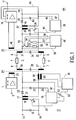
- reference numeral 1 designates a first signal processing device which is used, for example, for signal transmission in a telecommunications system between a connection 2 and a telecommunications line 3.
- the telecommunication line 3 is shown symbolically in FIG. 1 with two ohmic resistors 4, 5, which serve as equivalent circuit diagrams for the actual line impedances of the telecommunication line 3 and are arranged between line end connections 6, 7 and 8, 9, respectively.
- the line end connections 6, 7 form the end of the telecommunication line 3 facing the first signal processing device 1.
- the first signal processing device 1 is arranged, for example, in a telecommunication exchange from which at least one further signal processing device 10 is to be supplied with electrical energy.
- This further signal processing device 10 for example also a telecommunications device, is connected to a second line end formed by the line end connections 8, 9 and has a connection 11.
- telecommunications signals should be able to be transmitted from the connection 2 to the connection 11 and vice versa, the electrical circuit supplying the entire circuit arrangement exclusively from the location of the first signal processing device 1.
- a supply voltage source 12 for the remote supply of the further signal processing device 10 which supplies electrical energy, for example, from an energy supply network can be supplied via two network connections 13, 14.
- the supply voltage source 12 in the example according to FIG. 1 is set up as a switching power supply for generating a supply voltage from a (preferably rectified) mains voltage supplied via the mains connections 13, 14.
- energy from, for example, a central battery or the like can also be supplied via the mains connections 13, 14.
- the switched-mode power supply of the supply voltage source 12 comprises a first smoothing capacitor 15, which is arranged between the mains connections 13, 14, and a series circuit, arranged in parallel, of a primary winding 16 of a first switched-mode power supply transformer 17 with a first chopper switch 18.
- the first chopper switch 18 is shown in FIG. 1 Shown for the sake of simplicity as a mechanical switch, but in practice is preferably designed as an electronic switch. It is switched alternately into a conductive and a blocked state by a control circuit 19, for which purpose a control line 20 is used.
- An AC voltage is tapped from a secondary winding 21 of the first switched-mode power supply transformer 17 and fed to a series circuit comprising a first diode 22 with a second smoothing capacitor 23.
- the supply voltage is then tapped from the connections of the second smoothing capacitor 23 and fed to the line end connections 6 and 7 at the first line end connected to the first signal processing device 1.
- a first line transformer 24 is used to transmit the telecommunications signals between the first signal processing device 1 and the line end connections 6, 7 on the one hand and the electrical energy from the connections of the second smoothing capacitor 23 to the line end connections 6, 7 provided which comprises a primary winding 25 and a secondary winding divided into two parts 26, 27.
- first and the second part 26, 27 of the secondary winding of the first line transformer 24 are connected to the line end connection 6 or 7, whereas the other connections of the part 26, 27 of the secondary winding of the first line transformer 24 each have one of the connections of the second Smoothing capacitor 23 and also connected to each other via a first coupling capacitor 28.
- the first coupling capacitor 28 forms an AC short circuit for the signals to be transmitted from the telecommunication line 3 to the first signal processing device 1 and vice versa.
- the connections of the second smoothing capacitor 23 are also connected to two inputs 29, 30 of the control circuit 19.
- the power supply of the control circuit 19 is carried out via these inputs 29, 30; on the other hand, the voltage supplied via the inputs 29, 30 is used as a control variable for the formation of a control signal to the first chopper switch 18 via the control line 20.
- the control circuit 19 is preferably designed with a pulse width modulator which, via the control line 20, outputs a pulse width modulated pulse signal as a control signal to the first chopper switch 18, which controls it in such a way that the supply voltage at the second smoothing capacitor 23 is at least virtually constant regardless of the load.
- the signal processing device 10 on the second line end formed by the line end connections 8, 9 is likewise supplied with energy by a switching power supply which is fed remotely from the supply voltage source 12 via the telecommunication line 3.
- a switching power supply which is fed remotely from the supply voltage source 12 via the telecommunication line 3.
- the Line end connections 8, 9 at the second line end are bridged by a series connection of two parts 31, 32 of a secondary winding of a second line transformer 33 with a second coupling capacitor 34.
- the voltage losses in the telecommunication line 3 and the secondary windings 26, 27 or 31, 32 of the line transformers 24 or 33 weakened supply voltage tapped from the supply voltage source and fed to the switching power supply for remote supply of the signal processing device 10.
- This comprises a third smoothing capacitor 35 connected in parallel to the second coupling capacitor 34, to which, in turn, a series circuit comprising a primary winding 36 of a second switching power supply transformer 37 with a second chopper switch 38 is arranged in parallel.
- the second chopper switch 38 is switched alternately into the conductive and the blocked state by a second control circuit 39 via a second control line 40.
- a series circuit comprising a second diode 42 with a fourth smoothing capacitor 43 is connected to the connections of a secondary winding 41 of the second switching power supply transformer 37.
- the connections of the fourth smoothing capacitor 43 are tapped off from the supply voltage for the signal processing device 10 via power supply connections 44, 45.
- the fourth smoothing capacitor 43 is also connected with its connections to inputs 46 and 47 of the second control circuit 39, via which the voltage at the fourth smoothing capacitor 43 can be supplied as a supply voltage and at the same time as a measured variable.
- the function of the switching power supply 35 to 43 corresponds to that of the switching power supply 15 to 23 contained in the supply voltage source 12.
- the second line transformer 33 has a primary winding 48 which is magnetically coupled to the secondary winding 31, 32 in the same way as is the case with the first line transformer 24 between its primary winding 25 and its secondary winding 26, 27.
- the connections of the primary winding 48 of the second line transformer 33 are connected to the further signal processing device 10 in accordance with the connection of the connections of the primary winding 25 of the first line transformer 24 to the first signal processing device 1. Coupling and coupling of the telecommunication signals from the signal processing devices 1 and 10 to the telecommunication line 3 In this exemplary embodiment, this is preferably done symmetrically in order to create the same conditions in both transmission directions.
- the circuit arrangement at the second line end 8, 9, that is to say in connection with the remotely fed switching power supply 35 to 43, has a device for generating a characteristic signal which consists of an oscillation of a predeterminable frequency and which is emitted when it is transmitted via the second Line end 8, 9 supplied supply voltage at the second coupling capacitor 34 has a value which is lower than a predetermined reference voltage.
- Said device comprises a comparison stage 49, which is connected with two inputs 50, 51 in parallel to the second coupling capacitor 34 and the third smoothing capacitor 35, respectively. The supply voltage is fed to the comparison stage 49 via the inputs 50, 51.
- the comparison stage 49 is designed such that it is already at the supply voltage value, which is lower than the reference voltage and to which the supply voltage source 12 can be set, is ready for operation, regardless of whether the remote-fed switching power supply 35 to 43 or the signal processing device 10 supplied with energy can already operate at this supply voltage value.
- the supply voltage supplied via the inputs 50, 51 to the comparison stage 49 supplies the latter with electrical energy on the one hand and is used on the other hand for comparison with the predetermined reference voltage, which is preferably generated within the comparison stage 49.
- the described comparison can also be carried out, for example, between a certain fraction of this reference voltage and the same fraction of the supplied supply voltage, or threshold value circuits can be used which are dimensioned for the reference voltage.
- a series circuit comprising a first switch 52 with a first ohmic resistor 53 is arranged, which in turn is bridged by a series circuit comprising a second switch 54 with a second ohmic resistor 55.
- the comparison stage 49 has a first and a second control output 56 and 57, which are connected to the first and second switches 52 and 54, respectively. Via the first control output 56, the first switch 52 is brought into its conductive state by the comparison stage 49 if the supply voltage at the inputs 50, 51 of the comparison stage 49 is less than the reference voltage, and the first switch 52 is brought into its blocked state, if the supply voltage at the inputs 50, 51 the reference voltage exceeds.
- the switching stage 49 emits a switching signal with the frequency of the identification signal, by means of which the second switch 54 is alternately switched on or off.
- the first switch 52 is conductive, an oscillation is thus transmitted from the comparison stage 49 via the second switch 54 to the second line end 8, 9 and transported via the telecommunication line 3 to its first line end 6, 7.
- this identification signal is interrupted by the first switch 52.
- the supply voltage source 12 further comprises a characteristic signal transmitter 58, the primary winding 59 of which at one of its connections with the connection point between the first coupling capacitor and the second part 27 of the secondary winding of the first line transformer 24 and at a second connection with the connection point between the second smoothing capacitor 23, the secondary winding 21 of the first switching power supply transformer 17 and the input 29 of the first control circuit 19 is connected.
- the primary winding 59 of the identification signal transmitter 58 is thus arranged in the path of the supply current caused by the supply voltage from the supply voltage source 12, but not in the signal path for the telecommunications signals between the signal processing devices 1 and 10.
- the frequency of the identification signal is preferably selected to be lower than the frequencies comprised by the telecommunications signal, so that the identification signal is not short-circuited by the coupling capacitors 28, 34, in contrast to the telecommunications signal.
- a connection of a secondary winding 60 of the identification signal transmitter 58 is connected to an identification signal receiver 61. This is thus via the identification signal transmitter 58
- the identification signal is coupled out and sent to the identification signal receiver 61 for evaluation. If an identification signal, ie an oscillation of the predetermined frequency, is received by the latter, a switching signal is emitted at a switching output 62 of the identification signal receiver 61. This is fed to a changeover switch 63 connected to the switching output 62, the switch tongue and the changeover contacts of which are connected to the first control circuit 19. With the switching signal, the changeover switch 63 is transferred from a first switch position to a second switch position when a identification signal is received.
- the operation of the first chopper switch 18 is influenced in the control circuit 19 such that the supply voltage source 12 is set to deliver a preselected supply voltage with a value which is higher than the reference voltage.
- the changeover switch 63 remains in the position in which, controlled by the first control circuit 19, the supply voltage source 12 only outputs a supply voltage value which is lower than the reference voltage.
- the supply voltage source 12 When the circuit arrangement according to FIG. 1 is started up, also, for example, after an interruption in operation, the supply voltage source 12 will first emit a supply voltage with a value which is lower than the reference voltage. This supply voltage is fed via the telecommunication line 3 to the switching power supply 35 to 43 feeding the further signal processing device 10, but also to the comparison stage 49.
- the signal processing device 10 can be dimensioned for the supply voltage value assumed in this operating state; however, it is preferably dimensioned for a supply voltage value that is higher than the reference voltage. In the former case, the signal processing device 10 can already go into full operation, in the latter case it will not yet ready for use.
- the comparison stage 49 is already operational at the low supply voltage value and, via the second switch 54 and the second ohmic resistor 55, generates the identification signal, which is supplied via the first switch 52 in the telecommunication line 3 and thereby reaches the identification signal receiver 61 via the identification signal transmitter 58 .
- the comparison stage 49 is either completely omitted or no identification signal or an identification signal with a frequency which is not recognized by the identification signal receiver 61 as an identification signal for increasing the supply voltage .
- the further signal processing device 10 the second line transformer 33, the remotely fed switching power supply 35 to 43 and the device 49 to 57 for generating the identification signal form a load 64 connected to the second line end 8, 9.
- Loads ie signal processing devices, which can be remotely supplied with different supply voltage values, can also be distinguished from one another by identification signals with differently predetermined frequencies.
- signal processing devices can be classified for supply voltage values of 200 V, 300 V, 400 V, 600 V etc. Each of these classes is then assigned a characteristic frequency, that is to say a characteristic signal of predetermined, different frequencies.
- the comparison stage 49 with the ohmic resistors 53, 55 and the switches 52, 54, which forms a characteristic frequency generator, are then switched on by the switch 52 at a supply voltage value which is lower than the reference voltage, for example set at 120 V, and switched off at supply voltage values above 120 V.
- the supply voltage source 12 can be switched to its nominal supply voltage above 120 V. However, if the identification signal receiver 61 does not receive an identification signal or an identification signal with a different frequency, the supply voltage of the supply voltage source 12 remains less than 120 V. In addition, an error message can be output by the identification signal receiver 61 in this case.
- FIG. 2 which shows a second exemplary embodiment of the invention, corresponds in its elements serving for signal transmission and processing and remote feeding to that according to FIG. 1, so that it will not be discussed in more detail. It should only be mentioned that in the circuit arrangement according to FIG. 2 the third smoothing capacitor 35 is omitted or is combined with the second coupling capacitor 34.
- the circuit arrangement according to FIG. 2 has a comparison stage 490, to which the voltage provided by the remotely supplied switched-mode power supply at the fourth smoothing capacitor 43 is fed via a first and a second input 500 and 510, which also supplies the further via the power supply connections 44, 45 Signal processing device 10 feeds.
- the comparison stage 490 which can preferably be equipped with a microprocessor or a comparable control unit, has a control output 570 at which a digitally coded signal, for example a digitally coded signal Pulse signal, emitted and can be supplied to the further signal processing device 10 for transmission via the telecommunication line 3.
- This digital identification signal contains information about the supply voltage value for which the further signal processing device 10 is dimensioned.
- the supply voltage source 12 has a digital identification signal receiver 610, to which the identification signal received by the signal processing device 1 via the telecommunication line 3 is supplied via an identification signal line 611. By evaluating the supplied identification signal, a switching signal is generated in the digital identification signal receiver 610 and supplied to the changeover switch 63 via the switching output 62.
- the devices externally supplied as load 64 ie the further signal processing device 10, the second control circuit 39 and the comparison stage 490, are dimensioned such that they are ready for operation at a supply voltage value which is lower than the reference voltage. It is sufficient if the further signal processing device 10 is not yet fully operational for the transmission of all telecommunication signals to be exchanged with the first signal processing device 1, but is only able to transmit the identification signal from the comparison stage 490 via the telecommunication line 3 to the first signal processing device 1.
- the supply voltage source 12 is again operated in such a way that it only outputs the low supply voltage value below the reference voltage.
- the externally supplied switching power supply 36 to 43 at the second line end 8, 9 in Commissioned feeds the supply voltage generated by it via the inputs 500, 510 to the comparison stage 490 and via the power supply connections 44, 45 also to the further signal processing device 10.
- the applied supply voltage is compared by the comparison stage 490 with the reference voltage and, if it is lower than this, an identification signal, preferably as a digital code word and possibly periodically repeating, is sent via the control output 570 to the further signal processing device 10 which transmits this identification signal the telecommunication line 3 transmits the first signal processing device 1.
- the latter forwards the identification signal to the digital identification signal receiver 610 via the identification signal line 611.
- the evaluation of the identification signal in the digital identification signal receiver 610 provides information about whether the supply voltage source 12 can be switched over to a higher supply voltage value and possibly also about which of the different supply voltage values this switchover has to be carried out on. However, if the further signal processing device 10 is only dimensioned for the low supply voltage value below the reference voltage, this is also indicated via an appropriately coded identification signal - possibly also by the absence of an identification signal. The supply voltage source 12 is then operated at the low supply voltage value; if necessary, an error signal can again be emitted by the digital identification signal receiver 610. This type of identification signal can also be used to distinguish between loads that are dimensioned for different supply voltage values and to be fed correctly by remote control without the risk of damage from overvoltage.
Landscapes
- Engineering & Computer Science (AREA)
- Power Engineering (AREA)
- Computer Networks & Wireless Communication (AREA)
- Signal Processing (AREA)
- Physics & Mathematics (AREA)
- Electromagnetism (AREA)
- General Physics & Mathematics (AREA)
- Radar, Positioning & Navigation (AREA)
- Automation & Control Theory (AREA)
- Dc Digital Transmission (AREA)
- Direct Current Feeding And Distribution (AREA)
- Control Of Voltage And Current In General (AREA)
- Telephonic Communication Services (AREA)
- Dc-Dc Converters (AREA)
- Devices For Supply Of Signal Current (AREA)
Applications Claiming Priority (2)
| Application Number | Priority Date | Filing Date | Title |
|---|---|---|---|
| DE4434185A DE4434185A1 (de) | 1994-09-24 | 1994-09-24 | Schaltungsanordnung zum Speisen wenigstens einer Last |
| DE4434185 | 1994-09-24 |
Publications (2)
| Publication Number | Publication Date |
|---|---|
| EP0705020A2 true EP0705020A2 (fr) | 1996-04-03 |
| EP0705020A3 EP0705020A3 (fr) | 2000-03-22 |
Family
ID=6529117
Family Applications (1)
| Application Number | Title | Priority Date | Filing Date |
|---|---|---|---|
| EP95202474A Withdrawn EP0705020A3 (fr) | 1994-09-24 | 1995-09-13 | Circuit pour l'alimentation d'au moins une charge |
Country Status (5)
| Country | Link |
|---|---|
| US (1) | US5684391A (fr) |
| EP (1) | EP0705020A3 (fr) |
| JP (1) | JPH08214095A (fr) |
| DE (1) | DE4434185A1 (fr) |
| IL (1) | IL115377A (fr) |
Families Citing this family (8)
| Publication number | Priority date | Publication date | Assignee | Title |
|---|---|---|---|---|
| US7522878B2 (en) * | 1999-06-21 | 2009-04-21 | Access Business Group International Llc | Adaptive inductive power supply with communication |
| DE19955328C2 (de) * | 1999-11-17 | 2002-03-14 | Infineon Technologies Ag | Schaltungsanordnung zur Versorgung einer elektrischen Last mit elektrischer Leistung |
| US6806662B1 (en) * | 2003-05-28 | 2004-10-19 | The Boeing Company | Multiple mode universal power source utilizing a rotating machine |
| US7340051B2 (en) * | 2003-05-30 | 2008-03-04 | Adc Dsl Systems, Inc. | Power ramp-up in a line-powered network element system |
| SE526852C2 (sv) * | 2003-06-26 | 2005-11-08 | Kongsberg Automotive Ab | Metod och arrangemang för styrning av likströmsmotor |
| US7339809B2 (en) * | 2004-11-30 | 2008-03-04 | The Boeing Company | Systems and methods for electrical power regulation and distribution in aircraft |
| US7324772B2 (en) * | 2005-06-22 | 2008-01-29 | Xerox Corporation | Point-of-load design for high voltage AC power supplies |
| JP2012161117A (ja) * | 2011-01-28 | 2012-08-23 | Rohm Co Ltd | Dc/dcコンバータならびにそれを用いた電源装置および電子機器 |
Family Cites Families (4)
| Publication number | Priority date | Publication date | Assignee | Title |
|---|---|---|---|---|
| JPS60249832A (ja) * | 1984-05-25 | 1985-12-10 | 株式会社東芝 | インバ−タの保護方法 |
| US4626767A (en) * | 1984-12-21 | 1986-12-02 | Metcal, Inc. | Constant current r.f. generator |
| US4788455A (en) * | 1985-08-09 | 1988-11-29 | Mitsubishi Denki Kabushiki Kaisha | CMOS reference voltage generator employing separate reference circuits for each output transistor |
| JPH05137267A (ja) * | 1991-11-12 | 1993-06-01 | Dia Semikon Syst Kk | 電源装置 |
-
1994
- 1994-09-24 DE DE4434185A patent/DE4434185A1/de not_active Withdrawn
-
1995
- 1995-09-13 EP EP95202474A patent/EP0705020A3/fr not_active Withdrawn
- 1995-09-20 US US08/530,815 patent/US5684391A/en not_active Expired - Fee Related
- 1995-09-21 IL IL11537795A patent/IL115377A/en active IP Right Grant
- 1995-09-25 JP JP7246498A patent/JPH08214095A/ja active Pending
Non-Patent Citations (1)
| Title |
|---|
| None |
Also Published As
| Publication number | Publication date |
|---|---|
| EP0705020A3 (fr) | 2000-03-22 |
| US5684391A (en) | 1997-11-04 |
| JPH08214095A (ja) | 1996-08-20 |
| IL115377A0 (en) | 1995-12-31 |
| DE4434185A1 (de) | 1996-03-28 |
| IL115377A (en) | 1998-08-16 |
Similar Documents
| Publication | Publication Date | Title |
|---|---|---|
| DE3882635T2 (de) | Unterbrechungsfreie Stromversorgung. | |
| DE19533103B4 (de) | Schaltungsanordnung zum Betrieb einer Entladungslampe | |
| EP0261319B1 (fr) | Disposition de circuit pour produire une tension alternative | |
| DE69613445T2 (de) | Anordnung zur fernsteuerung und fernüberwachung einer entladungslampe | |
| EP3864743A1 (fr) | Dispositif et procédé de décharge d'un condensateur de circuit intermédiaire, convertisseur de courant et véhicule | |
| EP0705020A2 (fr) | Circuit pour l'alimentation d'au moins une charge | |
| DE68919664T2 (de) | Lastschalter für Elektrogeräte und Endgerät eines mit einem solchen Schalter versehenen Fernwirksystems. | |
| EP0803966A2 (fr) | Alimentation de puissance avec fonctionnement en mode veille | |
| DE3513625A1 (de) | Schaltungsanordnung fuer die fernspeisung von teilnehmeranschluss-endgeraeten in fernmeldeanlagen | |
| EP0671088A1 (fr) | Circuit pour la commande d'un ensemble de recepteurs, notamment de regulateurs de puissance de lampes. | |
| EP0139226A1 (fr) | Dispositif d'alimentation à convertisseur à récupération | |
| EP0299405B1 (fr) | Alimentation à découpage | |
| DE4330114B4 (de) | Schaltungsanordnung zum Steuern einer Mehrzahl von Verbrauchern, insbesondere Vorschaltgerät von Lampen | |
| DE19901196A1 (de) | Verfahren und Einrichtung zur Spannungsversorgung | |
| DE3633518A1 (de) | Getakteter gleichspannungswandler | |
| DE19758273B4 (de) | Notspeisefähige Stromversorgung für ISDN-Endsysteme | |
| EP0546625A1 (fr) | Dispositif de transmission d'impulsions de numérotation | |
| DE2755607C2 (fr) | ||
| DE3035515C2 (fr) | ||
| DE102019110666B3 (de) | Betriebsschaltung und Verfahren zum Betreiben wenigstens eines Geräts an einer Busleitung | |
| EP0717485A1 (fr) | Barrière de sécurité pour données à grand débit | |
| DE112016001109B4 (de) | Resonanzwandler mit einem transformator mit mittelpunktanzapfung | |
| LU505643B1 (de) | Energiemessgerät | |
| EP0499869B1 (fr) | Circuit pour génération de tension alternative | |
| EP1220433B1 (fr) | Alimentation pour un circuit de protection |
Legal Events
| Date | Code | Title | Description |
|---|---|---|---|
| PUAI | Public reference made under article 153(3) epc to a published international application that has entered the european phase |
Free format text: ORIGINAL CODE: 0009012 |
|
| AK | Designated contracting states |
Kind code of ref document: A2 Designated state(s): AT BE CH DE FR GB LI NL |
|
| RAP1 | Party data changed (applicant data changed or rights of an application transferred) |
Owner name: DEUTSCHE TELEKOM AG Owner name: PHILIPS ELECTRONICS N.V. Owner name: PHILIPS PATENTVERWALTUNG GMBH |
|
| RAP3 | Party data changed (applicant data changed or rights of an application transferred) |
Owner name: DEUTSCHE TELEKOM AG Owner name: KONINKLIJKE PHILIPS ELECTRONICS N.V. Owner name: PHILIPS CORPORATE INTELLECTUAL PROPERTY GMBH |
|
| PUAL | Search report despatched |
Free format text: ORIGINAL CODE: 0009013 |
|
| AK | Designated contracting states |
Kind code of ref document: A3 Designated state(s): AT BE CH DE FR GB LI NL |
|
| 17P | Request for examination filed |
Effective date: 20000922 |
|
| RAP1 | Party data changed (applicant data changed or rights of an application transferred) |
Owner name: DEUTSCHE TELEKOM AG Owner name: KONINKLIJKE PHILIPS ELECTRONICS N.V. Owner name: PHILIPS CORPORATE INTELLECTUAL PROPERTY GMBH |
|
| RAP1 | Party data changed (applicant data changed or rights of an application transferred) |
Owner name: DEUTSCHE TELEKOM AG Owner name: KONINKLIJKE PHILIPS ELECTRONICS N.V. Owner name: PHILIPS INTELLECTUAL PROPERTY & STANDARDS GMBH |
|
| 17Q | First examination report despatched |
Effective date: 20030812 |
|
| STAA | Information on the status of an ep patent application or granted ep patent |
Free format text: STATUS: THE APPLICATION IS DEEMED TO BE WITHDRAWN |
|
| 18D | Application deemed to be withdrawn |
Effective date: 20060401 |