EP0705051A1 - Taktrückgewinnung für einen ATM-Empfänger - Google Patents
Taktrückgewinnung für einen ATM-Empfänger Download PDFInfo
- Publication number
- EP0705051A1 EP0705051A1 EP95202376A EP95202376A EP0705051A1 EP 0705051 A1 EP0705051 A1 EP 0705051A1 EP 95202376 A EP95202376 A EP 95202376A EP 95202376 A EP95202376 A EP 95202376A EP 0705051 A1 EP0705051 A1 EP 0705051A1
- Authority
- EP
- European Patent Office
- Prior art keywords
- clock
- frequency
- cell
- bit rate
- cells
- Prior art date
- Legal status (The legal status is an assumption and is not a legal conclusion. Google has not performed a legal analysis and makes no representation as to the accuracy of the status listed.)
- Granted
Links
Images

Classifications
-
- H—ELECTRICITY
- H04—ELECTRIC COMMUNICATION TECHNIQUE
- H04Q—SELECTING
- H04Q11/00—Selecting arrangements for multiplex systems
- H04Q11/04—Selecting arrangements for multiplex systems for time-division multiplexing
- H04Q11/0428—Integrated services digital network, i.e. systems for transmission of different types of digitised signals, e.g. speech, data, telecentral, television signals
- H04Q11/0478—Provisions for broadband connections
-
- H—ELECTRICITY
- H04—ELECTRIC COMMUNICATION TECHNIQUE
- H04J—MULTIPLEX COMMUNICATION
- H04J3/00—Time-division multiplex systems
- H04J3/02—Details
- H04J3/06—Synchronising arrangements
- H04J3/062—Synchronisation of signals having the same nominal but fluctuating bit rates, e.g. using buffers
- H04J3/0632—Synchronisation of packets and cells, e.g. transmission of voice via a packet network, circuit emulation service [CES]
-
- H—ELECTRICITY
- H04—ELECTRIC COMMUNICATION TECHNIQUE
- H04L—TRANSMISSION OF DIGITAL INFORMATION, e.g. TELEGRAPHIC COMMUNICATION
- H04L12/00—Data switching networks
- H04L12/54—Store-and-forward switching systems
- H04L12/56—Packet switching systems
- H04L12/5601—Transfer mode dependent, e.g. ATM
- H04L2012/5614—User Network Interface
- H04L2012/5616—Terminal equipment, e.g. codecs, synch.
-
- H—ELECTRICITY
- H04—ELECTRIC COMMUNICATION TECHNIQUE
- H04L—TRANSMISSION OF DIGITAL INFORMATION, e.g. TELEGRAPHIC COMMUNICATION
- H04L12/00—Data switching networks
- H04L12/54—Store-and-forward switching systems
- H04L12/56—Packet switching systems
- H04L12/5601—Transfer mode dependent, e.g. ATM
- H04L2012/5672—Multiplexing, e.g. coding, scrambling
- H04L2012/5674—Synchronisation, timing recovery or alignment
Definitions
- the invention relates to an ATM receiver, in particular the clock recovery circuit.
- an ATM transmission system it is possible to transmit, via various virtual channels, source signals at different bit rates, as a result of which the number of ATM cells per unit time, the cell rate, may differ in the one virtual channel from that in another channel.
- the cells of a particular channel arrive at a receiver - allocated temporarily to said channel - said cells must, after having been incorporated in a buffer, be read out therefrom at a clock frequency which is consistent with the cell rate of that channel and with the bit rate (and clock frequency) of the source signal.
- the subject of the present invention is a circuit for deriving, from the cell arrival times, the clock frequency at which said buffer is read out. In the process it is necessary to allow for different nominal cell rates and for variations within those nominal cell rates. So far, the objective of detecting, in a satisfactory manner and entirely automatically, the clock frequency from the arrival times of ATM cells has not been met with a known solution.
- the invention comprises a clock recovery circuit for an ATM receiver, the clock frequency being derived entirely automatically from the cell arrival times.
- the circuit according to the invention comprises first means for determining, on the basis of the cell rate of the received cells, the nominal bit rate of the source signal and generating a clock signal having a frequency which is consistent therewith, and second means for correcting, in proportion to the difference between the nominal bit rate determined by the first means and the mean actual bit rate, the frequency of the clock signal generated by the first means.
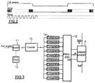
- Figure 1 shows an illustrative embodiment of the invention.
- Figure 2 depicts a number of signals.
- Figure 3 shows an illustrative embodiment of one of the units shown in Figure 1.
- the circuit shown in Figure 1 has been designed for automatic recovery of the source clock for source signals having bit rates of 64, 128, 144, 192, 256, 512, 1024 and 2048 kbits/sec.
- ATM cells are fed to a buffer 1 via an input circuit.
- a WRITE signal is composed for the cell buffer 1 from a network clock signal of 155.520 MHz (current standard for ATM networks) and a "cell enable" signal by means of which an ATM cell is admitted by the input circuit to buffer 1.
- Such a "cell enable” signal is produced, for example, by an access monitoring unit such as that described in patent EP - 381 275 B1 in the name of Applicant.
- the WRITE signal has a "burst" character (see also Figure 2).
- the rest of the circuit serves to produce a READ clock signal which corresponds to the cell rate of the cells presented to buffer 1 and which does not have a burst character (see also Figure 2).
- the frequency of that READ signal is equal to the bit rate of the source signal and therefore equal to the frequency of the source clock.
- the circuit includes a coarse adjustment for the clock frequency at which buffer 1 is read out, comprising a division factor adjustment 3 and a variable frequency divider 4.
- the circuit further includes a fine adjustment, comprising monostable multivibrators 6 and 7, an amplifier 8, a low-pass filter 9, 10 and a VCO (Voltage Controlled Oscillator).
- the division factor adjustment 3 is driven by the "cell enable" signal. After the time between two (or more) successive "cell enable” signals has been measured and the measured time has been categorized in accordance with the closest standard time which corresponds to one of the abovementioned bit rates, a division factor N which has been allocated to that closest standard time is presented to the frequency divider 4.
- the frequency divider 4 divides the frequency of the clock signal which is presented by the VCO 5 by factor N.
- the WRITE signal is also presented to a monostable multivibrator 7, which assigns a defined width to the WRITE pulses presented.
- the READ signal is presented to a monostable multivibrator 6 which ensures that the READ pulses are assigned a defined width.
- the two signals then pass to the + and - input, respectively, of an amplifier 8.
- a capacitor 10 via a resistor 9, is charged by the READ pulses and discharged by the WRITE pulses.
- the voltage U control over capacitor 9 drops, and the frequency of the VCO 5 is readjusted, as a result of which the READ clock frequency increases.
- FIG 3 shows a specific embodiment of the abovementioned unit 3 which calculates the division factor N.
- This unit comprises a NAND gate 11, a clock generator 12 and a counter 13.
- Counter 13 receives pulses from clock generator 12 during the period when there is no "cell enable" signal (see also Figure 2). If the cell rate is low, that period is relatively long and the counter attains a relatively high value; at a high cell rate, the counter reaches only a low value.
- the counter value reached is presented to a number of digital comparators 14 which are each set to a counter value which represents a specific nominal bit rate.
- the comparator 14 which has a counter value which is closest to the counter value reached by the counter 13 gives an indication to processor 15.
- Processor 15 calculates, on the basis of the position of that comparator, the value for N and passes this to the variable divider 4. In the case of a low cell rate, the counter 13 reaches a relatively high value, and the value of N likewise becomes relatively high, as a result of which the value of f ⁇ /N is relatively low.
Landscapes
- Engineering & Computer Science (AREA)
- Computer Networks & Wireless Communication (AREA)
- Multimedia (AREA)
- Computer Hardware Design (AREA)
- Signal Processing (AREA)
- Data Exchanges In Wide-Area Networks (AREA)
- Synchronisation In Digital Transmission Systems (AREA)
Applications Claiming Priority (2)
| Application Number | Priority Date | Filing Date | Title |
|---|---|---|---|
| NL9401525 | 1994-09-21 | ||
| NL9401525A NL9401525A (nl) | 1994-09-21 | 1994-09-21 | Clock recovery voor ATM ontvanger. |
Publications (2)
| Publication Number | Publication Date |
|---|---|
| EP0705051A1 true EP0705051A1 (de) | 1996-04-03 |
| EP0705051B1 EP0705051B1 (de) | 2001-04-04 |
Family
ID=19864672
Family Applications (1)
| Application Number | Title | Priority Date | Filing Date |
|---|---|---|---|
| EP95202376A Expired - Lifetime EP0705051B1 (de) | 1994-09-21 | 1995-09-04 | Taktrückgewinnung für einen ATM-Empfänger |
Country Status (8)
| Country | Link |
|---|---|
| US (1) | US5784379A (de) |
| EP (1) | EP0705051B1 (de) |
| JP (1) | JPH08111685A (de) |
| AT (1) | ATE200380T1 (de) |
| CA (1) | CA2158531C (de) |
| DE (1) | DE69520536T2 (de) |
| ES (1) | ES2155870T3 (de) |
| NL (1) | NL9401525A (de) |
Cited By (4)
| Publication number | Priority date | Publication date | Assignee | Title |
|---|---|---|---|---|
| EP0684740A3 (de) * | 1994-05-27 | 1997-09-24 | At & T Corp | Taktwiedergewinnung für Video mit variabler Bitrate in ATM-Netzwerken. |
| WO1998004063A3 (en) * | 1996-07-19 | 1998-03-12 | Ericsson Telefon Ab L M | A method and an apparatus for recovery of the clock of a constant bit-rate service |
| WO1999034638A1 (en) * | 1997-12-23 | 1999-07-08 | Nokia Networks Oy | Clock generating method and apparatus for an asynchronous transmission |
| WO2011019741A1 (en) * | 2009-08-10 | 2011-02-17 | Qualcomm Incorporated | Systems and methods for clock correction |
Families Citing this family (8)
| Publication number | Priority date | Publication date | Assignee | Title |
|---|---|---|---|---|
| NL9401696A (nl) | 1994-10-14 | 1996-05-01 | Nederland Ptt | Bufferuitleesbesturing van ATM ontvanger. |
| AU3864497A (en) * | 1997-08-06 | 1999-03-01 | Telefonaktiebolaget Lm Ericsson (Publ) | A method and an apparatus for the clock recovery in the transport of constant bit rate services over asynchronous transfer mode |
| JP3444397B2 (ja) * | 1998-02-06 | 2003-09-08 | ヤマハ株式会社 | ディジタル信号受信装置、方法、および該方法に係るプログラムを記憶した記憶媒体 |
| US6990109B2 (en) * | 2001-10-31 | 2006-01-24 | Adtran, Inc. | Method and apparatus for providing reliable voice and voice-band data transmission over asynchronous transfer mode (ATM) network |
| DE10232988B4 (de) | 2002-07-19 | 2007-11-22 | Infineon Technologies Ag | Verfahren und Vorrichtung zur getakteten Ausgabe asynchron empfangener Digitalsignale |
| DE10357477B4 (de) * | 2003-12-09 | 2008-11-06 | Nokia Siemens Networks Gmbh & Co.Kg | Schaltungsanordnung und Verfahren zur Taktsynchronisation |
| KR100606368B1 (ko) * | 2004-11-30 | 2006-07-31 | 엘지노텔 주식회사 | 에이티엠 수신기에서의 클럭 복구 장치 및 그 방법 |
| KR102472946B1 (ko) * | 2016-02-26 | 2022-12-05 | 에스케이하이닉스 주식회사 | 신호 복원 회로 |
Citations (3)
| Publication number | Priority date | Publication date | Assignee | Title |
|---|---|---|---|---|
| US4105946A (en) * | 1977-07-06 | 1978-08-08 | Sansui Electric Co., Ltd. | Frequency synthesizer with phase locked loop and counter |
| EP0577329A2 (de) * | 1992-07-02 | 1994-01-05 | AT&T Corp. | Taktwiedergewinnung für Video mit variabler Bite-Rate in Asynchronübertragungsnetzwerken |
| EP0381275B1 (de) | 1989-02-03 | 1994-03-30 | Koninklijke KPN N.V. | Verfahren zur Übertragung eines Flusses von Datenzellen, über eine Mehrzahl von Asynchron-Zeitmultiplex-Übertragungs-Kanälen, wobei der Stand eines Zählers für jeden Übertragungskanal in Übereinstimmung mit der Anzahl von Datenzellen pro Zeiteinheit auf dem laufenden gehalten wird |
Family Cites Families (9)
| Publication number | Priority date | Publication date | Assignee | Title |
|---|---|---|---|---|
| JPH03114333A (ja) * | 1989-09-28 | 1991-05-15 | Toshiba Corp | パケット伝送におけるクロック同期方式とパケット送信装置およびパケット受信装置 |
| JP2865782B2 (ja) * | 1990-03-16 | 1999-03-08 | 富士通株式会社 | 非同期伝送用codec装置 |
| JPH04362830A (ja) * | 1991-06-10 | 1992-12-15 | Oki Electric Ind Co Ltd | 音声パケット通信方式 |
| JPH04362827A (ja) * | 1991-06-10 | 1992-12-15 | Oki Electric Ind Co Ltd | パケット通信方式 |
| JPH05244113A (ja) * | 1992-02-27 | 1993-09-21 | Nec Corp | データ伝送装置 |
| JPH0630043A (ja) * | 1992-07-13 | 1994-02-04 | Nec Corp | 音声パケット通信方式 |
| JPH06152632A (ja) * | 1992-11-11 | 1994-05-31 | Oki Electric Ind Co Ltd | データ流量監視方法及びその装置 |
| JP3340162B2 (ja) * | 1992-12-07 | 2002-11-05 | 富士通株式会社 | ネットワーク間結合装置 |
| CA2127521C (en) * | 1994-07-06 | 2002-02-05 | Kenneth M. Buckland | Method and apparatus for recovering a variable bit rate service clock |
-
1994
- 1994-09-21 NL NL9401525A patent/NL9401525A/nl not_active Application Discontinuation
-
1995
- 1995-09-04 DE DE69520536T patent/DE69520536T2/de not_active Expired - Lifetime
- 1995-09-04 EP EP95202376A patent/EP0705051B1/de not_active Expired - Lifetime
- 1995-09-04 AT AT95202376T patent/ATE200380T1/de not_active IP Right Cessation
- 1995-09-04 ES ES95202376T patent/ES2155870T3/es not_active Expired - Lifetime
- 1995-09-07 US US08/525,302 patent/US5784379A/en not_active Expired - Lifetime
- 1995-09-18 CA CA002158531A patent/CA2158531C/en not_active Expired - Fee Related
- 1995-09-21 JP JP7242725A patent/JPH08111685A/ja active Pending
Patent Citations (3)
| Publication number | Priority date | Publication date | Assignee | Title |
|---|---|---|---|---|
| US4105946A (en) * | 1977-07-06 | 1978-08-08 | Sansui Electric Co., Ltd. | Frequency synthesizer with phase locked loop and counter |
| EP0381275B1 (de) | 1989-02-03 | 1994-03-30 | Koninklijke KPN N.V. | Verfahren zur Übertragung eines Flusses von Datenzellen, über eine Mehrzahl von Asynchron-Zeitmultiplex-Übertragungs-Kanälen, wobei der Stand eines Zählers für jeden Übertragungskanal in Übereinstimmung mit der Anzahl von Datenzellen pro Zeiteinheit auf dem laufenden gehalten wird |
| EP0577329A2 (de) * | 1992-07-02 | 1994-01-05 | AT&T Corp. | Taktwiedergewinnung für Video mit variabler Bite-Rate in Asynchronübertragungsnetzwerken |
Non-Patent Citations (1)
| Title |
|---|
| H.J.CHAO,C.A.JOHNSTON: "Asynchronous transfer mode packet video transmission system.", OPTICAL ENGINEERING, vol. 28, no. 7, BELLINGHAM US, pages 781 - 788, XP000033802 * |
Cited By (5)
| Publication number | Priority date | Publication date | Assignee | Title |
|---|---|---|---|---|
| EP0684740A3 (de) * | 1994-05-27 | 1997-09-24 | At & T Corp | Taktwiedergewinnung für Video mit variabler Bitrate in ATM-Netzwerken. |
| WO1998004063A3 (en) * | 1996-07-19 | 1998-03-12 | Ericsson Telefon Ab L M | A method and an apparatus for recovery of the clock of a constant bit-rate service |
| WO1999034638A1 (en) * | 1997-12-23 | 1999-07-08 | Nokia Networks Oy | Clock generating method and apparatus for an asynchronous transmission |
| US6876674B1 (en) | 1997-12-23 | 2005-04-05 | Nokia Corporation | Clock generating method and apparatus for an asynchronous transmission |
| WO2011019741A1 (en) * | 2009-08-10 | 2011-02-17 | Qualcomm Incorporated | Systems and methods for clock correction |
Also Published As
| Publication number | Publication date |
|---|---|
| CA2158531A1 (en) | 1996-03-22 |
| CA2158531C (en) | 2000-04-11 |
| ATE200380T1 (de) | 2001-04-15 |
| ES2155870T3 (es) | 2001-06-01 |
| US5784379A (en) | 1998-07-21 |
| DE69520536D1 (de) | 2001-05-10 |
| EP0705051B1 (de) | 2001-04-04 |
| NL9401525A (nl) | 1996-05-01 |
| JPH08111685A (ja) | 1996-04-30 |
| DE69520536T2 (de) | 2001-08-30 |
Similar Documents
| Publication | Publication Date | Title |
|---|---|---|
| US5784379A (en) | Clock recovery for ATM receiver | |
| CA2077017C (en) | Synchronous digital signal to asynchronous digital signal desynchronizer | |
| US4996698A (en) | Clock signal resynchronizing apparatus | |
| US5313502A (en) | Arrangement for imaging a useful signal from the frame of a first digital signal at a first bite rate into the frame of a second digital signal at a second bite rate | |
| US6157646A (en) | Circuit and method for service clock recovery | |
| EP0536464B1 (de) | Sonet DS-N-Desynchronisiereinrichtung | |
| US5052025A (en) | Synchronous digital signal to asynchronous digital signal desynchronizer | |
| US5361263A (en) | Transmission system for the synchronous digital hierarchy | |
| US6415006B2 (en) | Reducing waiting time jitter | |
| SE515335C2 (sv) | Hastighetskonverteringsanordning som kan fastställa en tranmissionshastighet alltefter önskan | |
| EP0218597A1 (de) | Rahmenaufbau zum multiplexieren einer mehrzahl von unterkanälen auf einem kanal mit fester geschwindigkeit. | |
| US5276688A (en) | Circuit arrangement for bit rate adjustment | |
| US5157651A (en) | Apparatus and method for determining line rates | |
| GB2229592A (en) | Phase detectors | |
| US20030076911A1 (en) | Receiver apparatus in stuffing synchronization system | |
| EP0163210B1 (de) | Verfahren und Anordnung zur Regelung der Signalpegelverstärkung für Zweitonmeterfrequenzempfänger | |
| US6876674B1 (en) | Clock generating method and apparatus for an asynchronous transmission | |
| US5070517A (en) | Method and circuit for retuning the frequency of a frequency source | |
| EP0707398A1 (de) | Einrichtung zur Steuerung des Pufferlesens für einen ATM-Empfänger | |
| US5832039A (en) | Data processing circuit | |
| US4774518A (en) | Loran-C signal phase tracking apparatus | |
| EP1030476B1 (de) | Messungen der Verzögerungsvariation vom regenerierten Datenuhrtakt und von den assozierten Datenpaketen | |
| CA2072695C (en) | Detecting location of time slot where data begins using pointer in justification or stuffing synchronous tdm | |
| US5548624A (en) | Destuff circuit for asynchronous digital signals | |
| US4317080A (en) | Signal monitor system |
Legal Events
| Date | Code | Title | Description |
|---|---|---|---|
| PUAI | Public reference made under article 153(3) epc to a published international application that has entered the european phase |
Free format text: ORIGINAL CODE: 0009012 |
|
| AK | Designated contracting states |
Kind code of ref document: A1 Designated state(s): AT BE CH DE DK ES FR GB GR IE IT LI LU NL PT SE |
|
| 17P | Request for examination filed |
Effective date: 19961004 |
|
| 17Q | First examination report despatched |
Effective date: 19980928 |
|
| RAP3 | Party data changed (applicant data changed or rights of an application transferred) |
Owner name: KONINKLIJKE KPN N.V. |
|
| GRAG | Despatch of communication of intention to grant |
Free format text: ORIGINAL CODE: EPIDOS AGRA |
|
| GRAG | Despatch of communication of intention to grant |
Free format text: ORIGINAL CODE: EPIDOS AGRA |
|
| GRAH | Despatch of communication of intention to grant a patent |
Free format text: ORIGINAL CODE: EPIDOS IGRA |
|
| GRAH | Despatch of communication of intention to grant a patent |
Free format text: ORIGINAL CODE: EPIDOS IGRA |
|
| GRAA | (expected) grant |
Free format text: ORIGINAL CODE: 0009210 |
|
| AK | Designated contracting states |
Kind code of ref document: B1 Designated state(s): AT BE CH DE DK ES FR GB GR IE IT LI LU NL PT SE |
|
| PG25 | Lapsed in a contracting state [announced via postgrant information from national office to epo] |
Ref country code: GR Free format text: LAPSE BECAUSE OF NON-PAYMENT OF DUE FEES Effective date: 20010404 Ref country code: AT Free format text: LAPSE BECAUSE OF FAILURE TO SUBMIT A TRANSLATION OF THE DESCRIPTION OR TO PAY THE FEE WITHIN THE PRESCRIBED TIME-LIMIT Effective date: 20010404 |
|
| REF | Corresponds to: |
Ref document number: 200380 Country of ref document: AT Date of ref document: 20010415 Kind code of ref document: T |
|
| REG | Reference to a national code |
Ref country code: CH Ref legal event code: NV Representative=s name: ISLER & PEDRAZZINI AG Ref country code: CH Ref legal event code: EP |
|
| REG | Reference to a national code |
Ref country code: IE Ref legal event code: FG4D |
|
| REF | Corresponds to: |
Ref document number: 69520536 Country of ref document: DE Date of ref document: 20010510 |
|
| REG | Reference to a national code |
Ref country code: ES Ref legal event code: FG2A Ref document number: 2155870 Country of ref document: ES Kind code of ref document: T3 |
|
| ITF | It: translation for a ep patent filed | ||
| PG25 | Lapsed in a contracting state [announced via postgrant information from national office to epo] |
Ref country code: PT Free format text: LAPSE BECAUSE OF FAILURE TO SUBMIT A TRANSLATION OF THE DESCRIPTION OR TO PAY THE FEE WITHIN THE PRESCRIBED TIME-LIMIT Effective date: 20010704 |
|
| ET | Fr: translation filed | ||
| PG25 | Lapsed in a contracting state [announced via postgrant information from national office to epo] |
Ref country code: LU Free format text: LAPSE BECAUSE OF NON-PAYMENT OF DUE FEES Effective date: 20010904 Ref country code: IE Free format text: LAPSE BECAUSE OF NON-PAYMENT OF DUE FEES Effective date: 20010904 |
|
| PG25 | Lapsed in a contracting state [announced via postgrant information from national office to epo] |
Ref country code: DK Free format text: LAPSE BECAUSE OF FAILURE TO SUBMIT A TRANSLATION OF THE DESCRIPTION OR TO PAY THE FEE WITHIN THE PRESCRIBED TIME-LIMIT Effective date: 20011011 |
|
| REG | Reference to a national code |
Ref country code: GB Ref legal event code: IF02 |
|
| PLBE | No opposition filed within time limit |
Free format text: ORIGINAL CODE: 0009261 |
|
| STAA | Information on the status of an ep patent application or granted ep patent |
Free format text: STATUS: NO OPPOSITION FILED WITHIN TIME LIMIT |
|
| 26N | No opposition filed | ||
| REG | Reference to a national code |
Ref country code: IE Ref legal event code: MM4A |
|
| REG | Reference to a national code |
Ref country code: CH Ref legal event code: PCAR Free format text: ISLER & PEDRAZZINI AG;POSTFACH 1772;8027 ZUERICH (CH) |
|
| PGFP | Annual fee paid to national office [announced via postgrant information from national office to epo] |
Ref country code: CH Payment date: 20080915 Year of fee payment: 14 |
|
| PGFP | Annual fee paid to national office [announced via postgrant information from national office to epo] |
Ref country code: NL Payment date: 20080915 Year of fee payment: 14 Ref country code: IT Payment date: 20080925 Year of fee payment: 14 |
|
| PGFP | Annual fee paid to national office [announced via postgrant information from national office to epo] |
Ref country code: ES Payment date: 20080929 Year of fee payment: 14 |
|
| PGFP | Annual fee paid to national office [announced via postgrant information from national office to epo] |
Ref country code: BE Payment date: 20081001 Year of fee payment: 14 |
|
| PGFP | Annual fee paid to national office [announced via postgrant information from national office to epo] |
Ref country code: SE Payment date: 20090915 Year of fee payment: 15 |
|
| BERE | Be: lapsed |
Owner name: KONINKLIJKE *KPN N.V. Effective date: 20090930 |
|
| REG | Reference to a national code |
Ref country code: NL Ref legal event code: V1 Effective date: 20100401 |
|
| REG | Reference to a national code |
Ref country code: CH Ref legal event code: PL |
|
| PG25 | Lapsed in a contracting state [announced via postgrant information from national office to epo] |
Ref country code: NL Free format text: LAPSE BECAUSE OF NON-PAYMENT OF DUE FEES Effective date: 20100401 |
|
| PG25 | Lapsed in a contracting state [announced via postgrant information from national office to epo] |
Ref country code: BE Free format text: LAPSE BECAUSE OF NON-PAYMENT OF DUE FEES Effective date: 20090930 |
|
| PG25 | Lapsed in a contracting state [announced via postgrant information from national office to epo] |
Ref country code: LI Free format text: LAPSE BECAUSE OF NON-PAYMENT OF DUE FEES Effective date: 20090930 Ref country code: CH Free format text: LAPSE BECAUSE OF NON-PAYMENT OF DUE FEES Effective date: 20090930 |
|
| PG25 | Lapsed in a contracting state [announced via postgrant information from national office to epo] |
Ref country code: IT Free format text: LAPSE BECAUSE OF NON-PAYMENT OF DUE FEES Effective date: 20090904 |
|
| REG | Reference to a national code |
Ref country code: SE Ref legal event code: EUG |
|
| REG | Reference to a national code |
Ref country code: ES Ref legal event code: FD2A Effective date: 20110715 |
|
| PG25 | Lapsed in a contracting state [announced via postgrant information from national office to epo] |
Ref country code: ES Free format text: LAPSE BECAUSE OF NON-PAYMENT OF DUE FEES Effective date: 20110705 |
|
| PG25 | Lapsed in a contracting state [announced via postgrant information from national office to epo] |
Ref country code: ES Free format text: LAPSE BECAUSE OF NON-PAYMENT OF DUE FEES Effective date: 20090905 |
|
| PG25 | Lapsed in a contracting state [announced via postgrant information from national office to epo] |
Ref country code: SE Free format text: LAPSE BECAUSE OF NON-PAYMENT OF DUE FEES Effective date: 20100905 |
|
| PGFP | Annual fee paid to national office [announced via postgrant information from national office to epo] |
Ref country code: DE Payment date: 20130919 Year of fee payment: 19 |
|
| PGFP | Annual fee paid to national office [announced via postgrant information from national office to epo] |
Ref country code: FR Payment date: 20130919 Year of fee payment: 19 Ref country code: GB Payment date: 20130919 Year of fee payment: 19 |
|
| REG | Reference to a national code |
Ref country code: DE Ref legal event code: R119 Ref document number: 69520536 Country of ref document: DE |
|
| GBPC | Gb: european patent ceased through non-payment of renewal fee |
Effective date: 20140904 |
|
| REG | Reference to a national code |
Ref country code: DE Ref legal event code: R119 Ref document number: 69520536 Country of ref document: DE Effective date: 20150401 |
|
| REG | Reference to a national code |
Ref country code: FR Ref legal event code: ST Effective date: 20150529 |
|
| PG25 | Lapsed in a contracting state [announced via postgrant information from national office to epo] |
Ref country code: GB Free format text: LAPSE BECAUSE OF NON-PAYMENT OF DUE FEES Effective date: 20140904 Ref country code: DE Free format text: LAPSE BECAUSE OF NON-PAYMENT OF DUE FEES Effective date: 20150401 |
|
| PG25 | Lapsed in a contracting state [announced via postgrant information from national office to epo] |
Ref country code: FR Free format text: LAPSE BECAUSE OF NON-PAYMENT OF DUE FEES Effective date: 20140930 |