EP0706112A2 - Daten-Eingangs/-Ausgangssteuerungseinheit für Schnittstelleneinrichtung einer Berührungstafel - Google Patents
Daten-Eingangs/-Ausgangssteuerungseinheit für Schnittstelleneinrichtung einer Berührungstafel Download PDFInfo
- Publication number
- EP0706112A2 EP0706112A2 EP95401616A EP95401616A EP0706112A2 EP 0706112 A2 EP0706112 A2 EP 0706112A2 EP 95401616 A EP95401616 A EP 95401616A EP 95401616 A EP95401616 A EP 95401616A EP 0706112 A2 EP0706112 A2 EP 0706112A2
- Authority
- EP
- European Patent Office
- Prior art keywords
- signal
- control
- response
- data
- touch panel
- Prior art date
- Legal status (The legal status is an assumption and is not a legal conclusion. Google has not performed a legal analysis and makes no representation as to the accuracy of the status listed.)
- Granted
Links
Images


Classifications
-
- G—PHYSICS
- G06—COMPUTING OR CALCULATING; COUNTING
- G06F—ELECTRIC DIGITAL DATA PROCESSING
- G06F1/00—Details not covered by groups G06F3/00 - G06F13/00 and G06F21/00
- G06F1/26—Power supply means, e.g. regulation thereof
- G06F1/32—Means for saving power
- G06F1/3203—Power management, i.e. event-based initiation of a power-saving mode
- G06F1/3234—Power saving characterised by the action undertaken
- G06F1/325—Power saving in peripheral device
- G06F1/3262—Power saving in digitizer or tablet
-
- G—PHYSICS
- G06—COMPUTING OR CALCULATING; COUNTING
- G06F—ELECTRIC DIGITAL DATA PROCESSING
- G06F1/00—Details not covered by groups G06F3/00 - G06F13/00 and G06F21/00
- G06F1/26—Power supply means, e.g. regulation thereof
- G06F1/32—Means for saving power
- G06F1/3203—Power management, i.e. event-based initiation of a power-saving mode
- G06F1/3206—Monitoring of events, devices or parameters that trigger a change in power modality
- G06F1/3209—Monitoring remote activity, e.g. over telephone lines or network connections
Definitions
- the present invention relates in general to a touch panel interface device, and more particularly to a data input/output control unit for the touch panel interface device in which a system control part is designed with a digital logic circuit for usefulness in a portable system, and a present mode is changed to a suspend mode after the lapse of a predetermined time period from the moment that no data is applied to a touch panel, to turn off supply power to the touch panel and stop a system operation, so that power consumption can be minimized and a battery can be lengthened in life, in particular in small, portable equipments such as a personal digitizer assistance (referred to hereinafter as PDA) and the like.
- PDA personal digitizer assistance
- the conventional touch panel interface device comprises a touch panel 1 for sensing coordinates of a point touched by a user's pen and generating an analog signal in accordance with the sensed result, a read only memory (referred to hereinafter as ROM) 5 for storing a control program for controlling a system operation, a micro controller 4 for executing the control program stored in the ROM 5 to control the system operation, an analog/digital (referred to hereinafter as A/D) converter 2 for converting the analog signal from the touch panel 1 into digital data in response to a control signal CS10 from the micro controller 4 and outputting the converted digital data to the micro controller 4, a switch 3 for turning on/off supply power to the touch panel 1 in response to a control signal CS20 from the micro controller 4, and a serial communication circuit 6 for performing a serial communication with other systems in an RS-232 manner in response to a control signal CS30 from the micro controller 4.
- A/D analog/digital
- the micro controller 4 Upon power-on, the micro controller 4 outputs the control signal CS10 to the A/D converter 2 according to the control program stored in the ROM 5 to sense input data.
- the micro controller 4 If no data is sensed, the micro controller 4 outputs the control signal CS20 to the switch 3 to turn off the supply power to the touch panel 1.
- the touch panel 1 In the case where data is applied to the touch panel 1 by the user's pen, the corresponding coordinates are sensed by the touch panel 1. Then, the touch panel 1 outputs the analog signal corresponding to the sensed coordinates to the A/D converter 2, which converts the analog signal into the digital data in response to the control signal CS10 from the micro controller 4 and outputs the converted digital data to the micro controller 4. Then, the micro controller 4 stores the digital data from the A/D converter 2 into a random access memory (referred to hereinafter as RAM), not shown.
- RAM random access memory
- the micro controller 4 transfers the data stored in the RAM and the control signal CS30 to the serial communication circuit 6 to perform data transmission and reception with other systems.
- the serial communication circuit 6 may include, for example, a universal asynchronous receiver/transmitter (UART). Then, the serial communication circuit 6 performs the serial communication with other systems in the RS-232 manner.
- the above-mentioned conventional touch panel interface device has a disadvantage in that an internal structure cannot be known because the micro controller and the ROM are provided on a single application/specific integrated circuit (referred to hereinafter as ASIC) chip in a manufacturing process. For this reason, it is difficult to perform precision control for system implementation. Further, power consumption is increased because the power is always supplied to the other blocks and the micro controller scans the data input continuously by means of the A/D converter. This results in a reduction in life of a battery, particularly in small, portable equipments such as a PDA and the like.
- ASIC application/specific integrated circuit
- the present invention has been made in view of the above problem, and it is an object of the present invention to provide a data input/output control unit for a touch panel interface device in which a micro controller/ROM ASIC chip is designed with a digital logic circuit for usefulness in a portable system, and a present mode is changed to a suspend mode after the lapse of a predetermined time period from the moment that no data is applied to a touch panel, to turn off supply power to the touch panel and stop a system operation, so that power consumption can be minimized and a battery can be lengthened in life, in particular in small, portable equipments such as a PDA and the like.
- the data input/output control unit comprises a touch panel for sensing coordinates of a point touched by a user's pen and generating an analog signal in accordance with the sensed result; data detection means for detecting input data to the touch panel; system control means for controlling a system operation in response to an output signal from the data detection means; switching means for turning on/off supply power to the touch panel in response to a first control signal from the system control means; analog/digital conversion means for converting the analog signal from the touch panel into digital data in response to a second control signal from the system control means and outputting the converted digital data to the system control means; and serial communication means for performing a serial communication with other systems in response to a third control signal from the system control means.
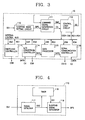
- the data input/output control unit comprises a touch panel 20 for sensing coordinates of a point touched by a user's pen and generating an analog signal in accordance with the sensed result, a data detector 40 for detecting input data to the touch panel 20 and outputting a detect signal DS1 in accordance with the detected result, a control circuit 10 for controlling a system operation in response to the detect signal DS1 from the data detector 40, and a switch 30 for turning on/off supply power to the touch panel 20 in response to a control signal CS8 from the control circuit 10.
- the data input/output control unit further comprises an A/D converter 50 for converting the analog signal from the touch panel 20 into digital data in response to a control signal CS9 from the control circuit 10 and outputting the converted digital data to the control circuit 10, and a serial communication circuit 60 for performing a serial communication with other systems in response to a control signal CS11 from the control circuit 10.
- A/D converter 50 for converting the analog signal from the touch panel 20 into digital data in response to a control signal CS9 from the control circuit 10 and outputting the converted digital data to the control circuit 10
- a serial communication circuit 60 for performing a serial communication with other systems in response to a control signal CS11 from the control circuit 10.
- the control circuit 10 includes a suspend mode setting circuit 110 for generating a suspend signal SPS in response to the detect signal DS1 from the data detector 40 to change a present mode to a suspend mode (power saving mode), and a command signal generation circuit 111 for generating a command signal CMS in response to a status signal SS and the suspend signal SPS from the suspend mode setting circuit 110 to control the system operation.
- the command signal generation circuit 111 also generates a status end signal ES upon its operation completion.
- the control circuit 10 further includes a control logic circuit 112 for analyzing the command signal CMS from the command signal generation circuit 111 in response to the status end signal ES therefrom and outputting control signals CS3-CS6 as a result of the analysis through an internal control bus line. Also, the control logic circuit 112 inputs response signals RS1-RS4 through the internal control bus line and outputs the status signal SS to the command signal generation circuit 111 in response to the inputted response signals RS1-RS4.
- the control circuit 10 further includes a switching controller 113 for outputting the control signal CS8 to the switch 30 in response to the control signal CS3 from the control logic circuit 112.
- the switching controller 113 also outputs the response signal RS1 to the control logic circuit 112 through the internal control bus line upon its operation completion.
- the control circuit 10 further includes an A/D conversion controller 114 for outputting the control signal CS9 to the A/D converter 50 in response to the control signal CS4 from the control logic circuit 112 and inputting the digital data from the A/D converter 50.
- the A/D conversion controller 114 also outputs the response signal RS2 to the control logic circuit 112 through the internal control bus line upon its operation completion.
- the control circuit 10 further includes a data processor 115 for processing output data from the A/D conversion controller 114 in response to the control signal CS5 from the control logic circuit 112 and outputting the response signal RS3 to the control logic circuit 112 through the internal control bus line upon its operation completion, and a serial communication controller 116 for applying output data from the data processor 115 and the control signal CS11 to the serial communication circuit 60 in response to the control signal CS6 from the control logic circuit 112.
- the serial communication controller 116 also outputs the response signal RS4 to the control logic circuit 112 through the internal control bus line upon its operation completion.
- the suspend mode setting circuit 110 includes a signal detector 117 for detecting the detect signal DS1 from the data detector 40 and outputting a detect signal DS2 in accordance with the detected result, a timer 118 for counting the detect signal DS2 from the signal detector 117 for a predetermined time period and outputting a control signal CS1 in accordance with the counted result, and a suspend signal generator 119 for outputting the suspend signal SPS to the command signal generation circuit 111 in response to the control signal CS1 from the timer 118.
- the command signal generation circuit 111 includes a status sensor 120 for sensing a present status in response to the status signal SS from the control logic circuit 112 and the suspend signal SPS from the suspend mode setting circuit 110, and an operation controller 121 for outputting an operation control signal CS2 in response to an output signal from the status sensor 120.
- the operation controller 121 also outputs the status end signal ES to the control logic circuit 112 upon its control operation completion.
- the command signal generation circuit 111 further includes a command generator 122 for outputting the command signal CMS to the control logic circuit 112 in response to the operation control signal CS2 from the operation controller 121.
- the command generator 122 includes a counter 126 for generating a table control signal S1 in response to the operation control signal CS2 from the operation controller 121, a command data memory 127 for storing command data in the form of table and outputting the stored command data in response to the operation control signal CS2 from the operation controller 121 and the table control signal S1 from the counter 126, and a decoder 128 for decoding output data from the command data memory 127 in response to the operation control signal CS2 from the operation controller 121 and outputting the resultant command signal CMS to the control logic circuit 112.
- the control logic circuit 112 includes a control signal distributor 123 being enabled in response to the status end signal ES from the command signal generation circuit 111 to analyze the command signal CMS from the command signal generation circuit 111 and output the resultant control signals CS3-CS6 through the internal control bus line to the switching controller 113, the A/D conversion controller 114, the data processor 115 and the serial communication controller 116, respectively.
- the control signal distributor 123 also outputs a control signal CS7 upon its operation completion.
- the control logic circuit 112 further includes a response signal transfer device 124 being enabled in response to the control signal CS7 from the control signal distributor 123 to input the response signal RS1 from the switching controller 113, the response signal RS2 from the A/D conversion controller 114, the response signal RS3 from the data processor 115 and the response signal RS4 from the serial communication controller 116 through the internal control bus line and transfer the inputted response signals RS1-RS4.
- a response signal transfer device 124 being enabled in response to the control signal CS7 from the control signal distributor 123 to input the response signal RS1 from the switching controller 113, the response signal RS2 from the A/D conversion controller 114, the response signal RS3 from the data processor 115 and the response signal RS4 from the serial communication controller 116 through the internal control bus line and transfer the inputted response signals RS1-RS4.
- the control logic circuit 112 further includes a status signal generator 125 for analyzing the response signals RS1-RS4 transferred by the response signal transfer device 124 and outputting the status signal SS to the command signal generation circuit 111 in accordance with the analyzed result.
- the touch panel 20 When data is applied to the touch panel 20 by the user's pen, the corresponding coordinates are sensed by the touch panel 20. Then, the touch panel 20 outputs the analog signal corresponding to the sensed coordinates to the A/D converter 50. At this time, the data detector 40 outputs the detect signal DS1 to the control circuit 10.
- the signal detector 117 detects the detect signal DS1 from the data detector 40 and outputs the resultant detect signal DS2 to the timer 118.
- the timer 118 Upon receiving the detect signal DS2 from the signal detector 117, the timer 118 does not generate the control signal CS1, so that the suspend signal generator 119 does not generate the suspend signal SPS.
- Such a status is sensed by the status sensor 120 in the command signal generation circuit 111. Then in the command signal generation circuit 111, the operation controller 121 generates the operation control signal CS2 in response to the sensed result from the status sensor 120.
- the operation control signal CS2 from the operation controller 121 is supplied to the command generator 122.
- the counter 126 outputs the table control signal S1 to the command data memory 127 in response to the operation control signal CS2 from the operation controller 121.
- the command data memory 127 outputs the command data stored in the form of table therein to the decoder 128 in response to the operation control signal CS2 from the operation controller 121 and the table control signal S1 from the counter 126.
- the decoder 128 decodes the output data from the command data memory 127 in response to the operation control signal CS2 from the operation controller 121 and outputs the resultant command signal CMS to the control logic circuit 112.
- the operation controller 121 then outputs the status end signal ES to the control logic circuit 112 at that time the control operation thereof is completed.
- control signal distributor 123 is enabled in response to the status end signal ES from the command signal generation circuit 111. As being enabled, the control signal distributor 123 analyzes the command signal CMS from the command signal generation circuit 111 and outputs the resultant control signals CS3-CS6 through the internal control bus line to the switching controller 113, the A/D conversion controller 114, the data processor 115 and the serial communication controller 116, respectively.
- the switching controller 113 Upon receiving the control signal CS3 from the control logic circuit 112, the switching controller 113 outputs the control signal CS8 to the switch 30 so that it can remain at its ON state.
- the control signal CS4 from the control logic circuit 112 enables the A/D conversion controller 114 to output the control signal CS9 to the A/D converter 50.
- the A/D converter 50 converts the analog signal from the touch panel 20 into the digital data and outputs the converted digital data to the A/D conversion controller 114, which then transfers the digital data from the A/D converter 50 to the data processor 115.
- the data processor 115 processes the transferred data from the A/D conversion controller 114 in response to the control signal CS5 from the control logic circuit 112 and outputs the processed data to the serial communication controller 116.
- the control signal CS6 from the control logic circuit 112 enables the serial communication controller 116 to apply the control signal CS11 and the output data from the data processor 115 to the serial communication circuit 60.
- the serial communication circuit 60 performs the serial communication with other systems in the RS-232 manner.
- the switching controller 113, the A/D conversion controller 114, the data processor 115 and the serial communication controller 116 output the response signals RS1-RS4 to the control logic circuit 112 through the internal control bus line at that time the operations thereof are completed.
- the control signal distributor 123 outputs the control signal CS7 to the response signal transfer device 124 at that time the operation thereof is completed.
- the response signal transfer device 124 is enabled in response to the control signal CS7 from the control signal distributor 123.
- the response signal transfer device 124 Upon receiving the response signal RS1 from the switching controller 113, the response signal RS2 from the A/D conversion controller 114, the response signal RS3 from the data processor 115 and the response signal RS4 from the serial communication controller 116 through the internal control bus line during being enabled, the response signal transfer device 124 transfers the inputted response signals RS1-RS4 to the status signal generator 125. Then, the status signal generator 125 analyzes the response signals RS1-RS4 transferred by the response signal transfer device 124 and outputs the status signal SS to the command signal generation circuit 111 in accordance with the analyzed result.
- the above operation is continuously repeated in the same manner as that previously mentioned.
- the same command signal CMS from the command signal generation circuit 111 is applied to the control logic circuit 112, thereby causing the control logic circuit 112 to output the control signals CS3-CS6 through the internal control bus line to the switching controller 113, the A/D conversion controller 114, the data processor 115 and the serial communication controller 116, respectively.
- the input data to the touch panel 20 is transferred to the serial communication circuit 60 through the A/D converter 50, the A/D conversion controller 114, the data processor 115 and the serial communication controller 116.
- the serial communication circuit 60 performs the serial communication with other systems in the RS-232 manner.
- the detect signal DS1 is not generated by the data detector 40, so that the detect signal DS2 is not generated by the signal detector 117 in the suspend mode setting circuit 110.
- the timer 118 outputs the control signal CS1 to the suspend signal generator 119 because it inputs no signal from the signal detector 117.
- the suspend signal generator 119 outputs the suspend signal SPS to the command signal generation circuit 111.
- the command signal generation circuit 111 Upon the suspend signal SPS from the suspend mode setting circuit 110, the command signal generation circuit 111 generates the command signal CMS for changing the present mode to the suspend mode. Then, the command signal generation circuit 111 outputs the generated command signal CMS together with the status end signal ES to the control signal distributor 123 in the control logic circuit 112. As being enabled in response to the status end signal ES from the command signal generation circuit 111, the control signal distributor 123 analyzes the received command signal CMS and outputs the resultant control signal CS3 to the switch controller 113 through the internal control bus line to change the present mode to the suspend mode.
- the switch controller 113 outputs the control signal CS8 to the switch 30 in response to the control signal CS3 from the control signal distributor 123, thereby causing the switch 30 to turn off the supply power to the touch panel 20.
- the A/D conversion controller 114, the data processor 115 and the serial communication controller 116 are stopped in operation, with the present mode changed to the suspend mode or the power saving mode.
- the data detector 40 outputs the detect signal DS1 to the suspend mode setting circuit 110 in the control circuit 10 so that the suspend signal SPS cannot be generated. As a result, the suspend mode is released.
- the command signal generation circuit 111 applies the command signal CMS and the status end signal ES to the control logic circuit 112.
- the control signal distributor 123 in the control logic circuit 112 analyzes the received command signal CMS and outputs the resultant control signal CS3 to the switch controller 113 through the internal control bus line.
- the switch controller 113 outputs the control signal CS8 to the switch 30 in response to the control signal CS3 from the control signal distributor 123, thereby causing the switch 30 to turn on the supply power to the touch panel 20.
- the input data to the touch panel 20 is transferred to the serial communication circuit 60 through the A/D converter 50, the A/D conversion controller 114, the data processor 115 and the serial communication controller 116.
- the serial communication circuit 60 performs the serial communication with other systems in the RS-232 manner.
- a micro controller/ROM ASIC chip is designed with the digital logic circuit for usefulness in a portable system. Also, the present mode is changed to the suspend mode after the lapse of the predetermined time period from the moment that no data is applied to the touch panel, to turn off the supply power to the touch panel and stop the system operation. Therefore, power consumption can be minimized and a battery can be lengthened in life, in particular in small, portable equipments such as a PDA and the like.
Landscapes
- Engineering & Computer Science (AREA)
- Theoretical Computer Science (AREA)
- Physics & Mathematics (AREA)
- General Engineering & Computer Science (AREA)
- General Physics & Mathematics (AREA)
- Position Input By Displaying (AREA)
Applications Claiming Priority (4)
| Application Number | Priority Date | Filing Date | Title |
|---|---|---|---|
| KR1019940025731A KR970010635B1 (ko) | 1994-10-07 | 1994-10-07 | 터치 판넬 인터페이스 장치의 데이타 입출력 제어 회로 |
| KR2573194 | 1994-10-07 | ||
| KR1019940031924A KR970008515B1 (ko) | 1994-11-30 | 1994-11-30 | 절전을 위한 터치 판넬 인터페이스 장치 |
| KR3192494 | 1994-11-30 |
Publications (3)
| Publication Number | Publication Date |
|---|---|
| EP0706112A2 true EP0706112A2 (de) | 1996-04-10 |
| EP0706112A3 EP0706112A3 (de) | 1996-10-30 |
| EP0706112B1 EP0706112B1 (de) | 2001-11-07 |
Family
ID=26630606
Family Applications (1)
| Application Number | Title | Priority Date | Filing Date |
|---|---|---|---|
| EP95401616A Expired - Lifetime EP0706112B1 (de) | 1994-10-07 | 1995-07-05 | Daten-Eingangs/-Ausgangssteuerungseinheit für Schnittstelleneinrichtung einer Berührungstafel |
Country Status (3)
| Country | Link |
|---|---|
| US (1) | US5621437A (de) |
| EP (1) | EP0706112B1 (de) |
| DE (1) | DE69523713T2 (de) |
Cited By (4)
| Publication number | Priority date | Publication date | Assignee | Title |
|---|---|---|---|---|
| WO1998053389A1 (en) * | 1997-05-22 | 1998-11-26 | Ericsson Inc. | Adaptive sampling of touch screen input |
| KR100825727B1 (ko) | 2005-12-07 | 2008-04-29 | 한국전자통신연구원 | 직렬 버스를 이용한 아날로그 신호의 디지털 변환 데이터수집 장치 및 그 방법 |
| WO2008136551A1 (en) * | 2007-05-02 | 2008-11-13 | Melfas, Inc. | Sleep mode wake-up method and sleep mode wake-up apparatus using touch sensing pad for use in an electronic device |
| CN108665844A (zh) * | 2018-05-21 | 2018-10-16 | 京东方科技集团股份有限公司 | 显示装置及其驱动方法、驱动装置 |
Families Citing this family (14)
| Publication number | Priority date | Publication date | Assignee | Title |
|---|---|---|---|---|
| US5719920A (en) * | 1995-03-31 | 1998-02-17 | The Messenger Group Llc | Method and apparatus for processing and downloading sound messages onto a permanent memory of a communication package |
| US6131047A (en) * | 1997-12-30 | 2000-10-10 | Ericsson Inc. | Radiotelephones having contact-sensitive user interfaces and methods of operating same |
| JPH11202998A (ja) * | 1998-01-08 | 1999-07-30 | Fujitsu Takamisawa Component Ltd | 情報処理装置 |
| JP2001147106A (ja) * | 1999-11-24 | 2001-05-29 | Namco Ltd | 受光パターン検出装置 |
| JP4397097B2 (ja) * | 2000-04-18 | 2010-01-13 | パナソニック株式会社 | プラズマディスプレイ装置 |
| KR20040062289A (ko) * | 2003-01-02 | 2004-07-07 | 삼성전자주식회사 | 휴대용 컴퓨터 및 그 제어방법 |
| KR100737887B1 (ko) * | 2003-05-20 | 2007-07-10 | 삼성전자주식회사 | 구동회로, 이를 갖는 평판표시장치 및 이의 구동방법 |
| KR101171185B1 (ko) * | 2005-09-21 | 2012-08-06 | 삼성전자주식회사 | 접촉 감지 기능이 있는 표시 장치, 그 구동 장치 및 방법 |
| KR101261610B1 (ko) * | 2006-02-24 | 2013-05-06 | 삼성디스플레이 주식회사 | 표시 장치 및 접촉 판단부의 제어 방법 |
| KR101613327B1 (ko) * | 2009-02-27 | 2016-04-18 | 가부시키가이샤 재팬 디스프레이 | 표시 장치, 터치 패널 및 전자 기기 |
| KR101831147B1 (ko) * | 2010-04-28 | 2018-02-26 | 가부시키가이샤 한도오따이 에네루기 켄큐쇼 | 반도체 표시 장치 및 그 구동 방법 |
| TWI443557B (zh) * | 2010-09-30 | 2014-07-01 | Wintek Corp | 觸控面板資料傳輸方法 |
| JP6012437B2 (ja) * | 2012-11-29 | 2016-10-25 | シナプティクス・ジャパン合同会社 | 半導体装置及び電子機器 |
| US11693515B2 (en) * | 2017-04-17 | 2023-07-04 | Sitronix Technology Corp. | Touch module and touch circuit thereof |
Family Cites Families (5)
| Publication number | Priority date | Publication date | Assignee | Title |
|---|---|---|---|---|
| US4922450A (en) * | 1987-10-08 | 1990-05-01 | Rose Frederick A | Communications management system having multiple power control modes |
| JPH02178817A (ja) * | 1988-12-29 | 1990-07-11 | Nec Home Electron Ltd | 携帯型電子機器 |
| JPH0496816A (ja) * | 1990-08-15 | 1992-03-30 | Ricoh Co Ltd | タッチパネル制御方式 |
| JP3193039B2 (ja) * | 1990-11-20 | 2001-07-30 | キヤノン株式会社 | 電子装置及び情報処理方法 |
| CA2059498A1 (en) * | 1991-01-22 | 1992-07-23 | Hideki Takahara | Data input and display apparatus |
-
1995
- 1995-07-05 EP EP95401616A patent/EP0706112B1/de not_active Expired - Lifetime
- 1995-07-05 US US08/498,465 patent/US5621437A/en not_active Expired - Lifetime
- 1995-07-05 DE DE69523713T patent/DE69523713T2/de not_active Expired - Lifetime
Non-Patent Citations (1)
| Title |
|---|
| None |
Cited By (8)
| Publication number | Priority date | Publication date | Assignee | Title |
|---|---|---|---|---|
| WO1998053389A1 (en) * | 1997-05-22 | 1998-11-26 | Ericsson Inc. | Adaptive sampling of touch screen input |
| US5977957A (en) * | 1997-05-22 | 1999-11-02 | Ericsson Inc. | Adaptive sampling of touch screen input |
| CN1110736C (zh) * | 1997-05-22 | 2003-06-04 | 艾利森公司 | 触摸屏输入的自适应抽样 |
| KR100825727B1 (ko) | 2005-12-07 | 2008-04-29 | 한국전자통신연구원 | 직렬 버스를 이용한 아날로그 신호의 디지털 변환 데이터수집 장치 및 그 방법 |
| US7453380B2 (en) | 2005-12-07 | 2008-11-18 | Electronics And Telecommunications Research Institute | Apparatus and method for processing analog signals and outputting digitally converted analog signals using serial bus |
| WO2008136551A1 (en) * | 2007-05-02 | 2008-11-13 | Melfas, Inc. | Sleep mode wake-up method and sleep mode wake-up apparatus using touch sensing pad for use in an electronic device |
| CN108665844A (zh) * | 2018-05-21 | 2018-10-16 | 京东方科技集团股份有限公司 | 显示装置及其驱动方法、驱动装置 |
| CN108665844B (zh) * | 2018-05-21 | 2021-05-14 | 京东方科技集团股份有限公司 | 显示装置及其驱动方法、驱动装置 |
Also Published As
| Publication number | Publication date |
|---|---|
| EP0706112A3 (de) | 1996-10-30 |
| US5621437A (en) | 1997-04-15 |
| EP0706112B1 (de) | 2001-11-07 |
| DE69523713D1 (de) | 2001-12-13 |
| DE69523713T2 (de) | 2002-07-25 |
Similar Documents
| Publication | Publication Date | Title |
|---|---|---|
| EP0706112B1 (de) | Daten-Eingangs/-Ausgangssteuerungseinheit für Schnittstelleneinrichtung einer Berührungstafel | |
| US8913017B2 (en) | Touch sensing system, electronic touch apparatus, and touch sensing method | |
| EP0996052A3 (de) | Eingabeverarbeitungsverfahren und Vorrichtung zur Eingabesteuerung | |
| KR20090071517A (ko) | 컴퓨터 시스템 | |
| JPH09231006A (ja) | 携帯情報処理装置 | |
| US5241646A (en) | Systems for changing hardware parameters using sub-CPU for sensing specialized key inputs and main CPU for changes | |
| JPH04308916A (ja) | 位置検出装置 | |
| CN113377444A (zh) | 一种基于触控按键唤醒的多模式切换方法 | |
| KR100553878B1 (ko) | 터치패널용 컴퓨팅장치의 객체상태 갱신장치 및 그에 따른 방법 | |
| KR20020081015A (ko) | 터치 인식과 필기체 인식 기능을 내장한 터치스크린프로세서 | |
| KR19990059505A (ko) | 휴대 정보 단말기를 이용한 펜입력 방법 및 장치 | |
| JPH0682314B2 (ja) | キ−ボ−ド同時打鍵シフト処理方式 | |
| KR950704756A (ko) | 단일-기능성 응용 소프트웨어와 하위 호환가능한 다중-기능성 사용자-인터페이스(Multi-functionality user-interface downwards compatible with single-functionality application software) | |
| JPH1153100A (ja) | ダブルタップ入力の補助方式 | |
| CN207851699U (zh) | 一种基于安卓系统的触控一体机 | |
| KR970010635B1 (ko) | 터치 판넬 인터페이스 장치의 데이타 입출력 제어 회로 | |
| KR970022693A (ko) | 터치 확인을 표시하는 터치 스크린 채용 제어 장치 및 그 제어 방법 | |
| TW257852B (en) | Coordinates detecting device | |
| TW256890B (en) | Detecting method and device for CPU executing efficiency | |
| KR970066815A (ko) | 피엘씨(plc)의 멀티 입력용 장치 및 방법 | |
| TW370639B (en) | Device and method of a write-protected basic input output system memory | |
| KR20000032560A (ko) | 터치 패널의 잡음 배제용 인식장치 | |
| JP2013254322A (ja) | 静電容量方式タッチパネル位置検出装置 | |
| JP2000099252A (ja) | デジタイザ情報出力装置 | |
| JPS62121638U (de) |
Legal Events
| Date | Code | Title | Description |
|---|---|---|---|
| PUAI | Public reference made under article 153(3) epc to a published international application that has entered the european phase |
Free format text: ORIGINAL CODE: 0009012 |
|
| AK | Designated contracting states |
Kind code of ref document: A2 Designated state(s): DE FR GB |
|
| PUAL | Search report despatched |
Free format text: ORIGINAL CODE: 0009013 |
|
| AK | Designated contracting states |
Kind code of ref document: A3 Designated state(s): DE FR GB |
|
| 17P | Request for examination filed |
Effective date: 19970318 |
|
| 17Q | First examination report despatched |
Effective date: 20000308 |
|
| GRAG | Despatch of communication of intention to grant |
Free format text: ORIGINAL CODE: EPIDOS AGRA |
|
| GRAG | Despatch of communication of intention to grant |
Free format text: ORIGINAL CODE: EPIDOS AGRA |
|
| GRAH | Despatch of communication of intention to grant a patent |
Free format text: ORIGINAL CODE: EPIDOS IGRA |
|
| GRAH | Despatch of communication of intention to grant a patent |
Free format text: ORIGINAL CODE: EPIDOS IGRA |
|
| GRAA | (expected) grant |
Free format text: ORIGINAL CODE: 0009210 |
|
| AK | Designated contracting states |
Kind code of ref document: B1 Designated state(s): DE FR GB |
|
| REF | Corresponds to: |
Ref document number: 69523713 Country of ref document: DE Date of ref document: 20011213 |
|
| REG | Reference to a national code |
Ref country code: GB Ref legal event code: IF02 |
|
| ET | Fr: translation filed | ||
| PLBE | No opposition filed within time limit |
Free format text: ORIGINAL CODE: 0009261 |
|
| STAA | Information on the status of an ep patent application or granted ep patent |
Free format text: STATUS: NO OPPOSITION FILED WITHIN TIME LIMIT |
|
| 26N | No opposition filed | ||
| PGFP | Annual fee paid to national office [announced via postgrant information from national office to epo] |
Ref country code: GB Payment date: 20140611 Year of fee payment: 20 |
|
| PGFP | Annual fee paid to national office [announced via postgrant information from national office to epo] |
Ref country code: DE Payment date: 20140611 Year of fee payment: 20 |
|
| PGFP | Annual fee paid to national office [announced via postgrant information from national office to epo] |
Ref country code: FR Payment date: 20140611 Year of fee payment: 20 |
|
| REG | Reference to a national code |
Ref country code: DE Ref legal event code: R071 Ref document number: 69523713 Country of ref document: DE |
|
| REG | Reference to a national code |
Ref country code: GB Ref legal event code: PE20 Expiry date: 20150704 |
|
| PG25 | Lapsed in a contracting state [announced via postgrant information from national office to epo] |
Ref country code: GB Free format text: LAPSE BECAUSE OF EXPIRATION OF PROTECTION Effective date: 20150704 |