US5621437A - Data input/output control unit for touch panel interface device - Google Patents
Data input/output control unit for touch panel interface device Download PDFInfo
- Publication number
- US5621437A US5621437A US08/498,465 US49846595A US5621437A US 5621437 A US5621437 A US 5621437A US 49846595 A US49846595 A US 49846595A US 5621437 A US5621437 A US 5621437A
- Authority
- US
- United States
- Prior art keywords
- signal
- control
- response
- data
- touch panel
- Prior art date
- Legal status (The legal status is an assumption and is not a legal conclusion. Google has not performed a legal analysis and makes no representation as to the accuracy of the status listed.)
- Expired - Lifetime
Links
Images


Classifications
-
- G—PHYSICS
- G06—COMPUTING OR CALCULATING; COUNTING
- G06F—ELECTRIC DIGITAL DATA PROCESSING
- G06F1/00—Details not covered by groups G06F3/00 - G06F13/00 and G06F21/00
- G06F1/26—Power supply means, e.g. regulation thereof
- G06F1/32—Means for saving power
- G06F1/3203—Power management, i.e. event-based initiation of a power-saving mode
- G06F1/3234—Power saving characterised by the action undertaken
- G06F1/325—Power saving in peripheral device
- G06F1/3262—Power saving in digitizer or tablet
-
- G—PHYSICS
- G06—COMPUTING OR CALCULATING; COUNTING
- G06F—ELECTRIC DIGITAL DATA PROCESSING
- G06F1/00—Details not covered by groups G06F3/00 - G06F13/00 and G06F21/00
- G06F1/26—Power supply means, e.g. regulation thereof
- G06F1/32—Means for saving power
- G06F1/3203—Power management, i.e. event-based initiation of a power-saving mode
- G06F1/3206—Monitoring of events, devices or parameters that trigger a change in power modality
- G06F1/3209—Monitoring remote activity, e.g. over telephone lines or network connections
Definitions
- the present invention relates in general to a touch panel interface device, and more particularly to a data input/output control unit for the touch panel interface device in which a system control part is designed with a digital logic circuit for use in a portable system, and a present mode is changed to a suspend mode after the lapse of a predetermined time period from the moment that no data is applied to a touch panel, to turn off supply power to the touch panel and stop a system operation, so that power consumption can be minimized and a battery can be lengthened in life, in particular in small, portable equipments such as a personal digitizer assistant (referred to hereinafter as PDA) and the like.
- PDA personal digitizer assistant
- the conventional touch panel interface device comprises a touch panel 1 for sensing coordinates of a point touched by a user's pen and generating an analog signal in accordance with the sensed result, a read only memory (referred to hereinafter as ROM) 5 for storing a control program for controlling a system operation, a micro controller 4 for executing the control program stored in the ROM 5 to control the system operation, an analog/digital (referred to hereinafter as A/D) converter 2 for converting the analog signal from the touch panel 1 into digital data in response to a control signal CS10 from the micro controller 4 and outputting the converted digital data to the micro controller 4, a switch 3 for turning on/off supply power to the touch panel 1 in response to a control signal CS20 from the micro controller 4, and a serial communication circuit 6 for performing a serial communication with other systems in an RS-232 manner in response to a control signal CS30 from the micro controller 4.
- A/D analog/digital
- the micro controller 4 Upon power-on, the micro controller 4 outputs the control signal CS10 to the A/D converter 2 according to the control program stored in the ROM 5 to sense input data.
- the micro controller 4 If no data is sensed, the micro controller 4 outputs the control signal CS20 to the switch 3 to turn off the supply power to the touch panel 1.
- the touch panel 1 In the case where data is applied to the touch panel 1 by the user's pen, the corresponding coordinates are sensed by the touch panel 1. Then, the touch panel 1 outputs the analog signal corresponding to the sensed coordinates to the A/D converter 2, which converts the analog signal into the digital data in response to the control signal CS10 from the micro controller 4 and outputs the converted digital data to the micro controller 4. Then, the micro controller 4 stores the digital data from the A/D converter 2 into a random access memory (referred to hereinafter as RAM), not shown.
- RAM random access memory
- the micro controller 4 transfers the data stored in the RAM and the control signal CS30 to the serial communication circuit 6 to perform data transmission and reception with other systems.
- the serial communication circuit 6 may include, for example, a universal asynchronous receiver/transmitter (UART). Then, the serial communication circuit 6 performs the serial communication with other systems in the RS-232 manner.
- the above-mentioned conventional touch panel interface device has a disadvantage in that an internal structure cannot be known because the micro controller and the ROM are provided on a single application/specific integrated circuit (referred to hereinafter as ASIC) chip in a manufacturing process. For this reason, it is difficult to perform precision control for system implementation. Further, power consumption is increased because the power is always supplied to the other blocks and the micro controller scans the data input continuously by means of the A/D converter. This results in a reduction in life of a battery, particularly in small, portable equipments such as a PDA and the like.
- ASIC application/specific integrated circuit
- the present invention has been made in view of the above problem, and it is an object of the present invention to provide a data input/output control unit for a touch panel interface device in which a micro controller/ROM ASIC chip is designed with a digital logic circuit for use in a portable system, and a present mode is changed to a suspend mode after the lapse of a predetermined time period from the moment that no data is applied to a touch panel in order to turn off supply power to the touch panel and stop a system operation, so that power consumption can be minimized and a battery can be lengthened in life, in particular in small, portable equipments such as a PDA and the like.
- the data input/output control unit comprises a touch panel for sensing coordinates of a point touched by a user's pen and generating an analog signal in accordance with the sensed result; data detection means for detecting input data to the touch panel; system control means for controlling a system operation in response to an output signal from the data detection means; switching means for turning on/off supply power to the touch panel in response to a first control signal from the system control means; analog/digital conversion means for converting the analog signal from the touch panel into digital data in response to a second control signal from the system control means and outputting the converted digital data to the system control means; and serial communication means for performing a serial communication with other systems in response to a third control signal from the system control means.
- FIG. 1 is a schematic block diagram of a conventional touch panel interface device
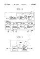
- FIG. 2 is a schematic block diagram of a data input/output control unit for a touch panel interface device in accordance with the present invention
- FIG. 3 is a detailed block diagram of the control circuit in FIG. 2;
- FIG. 4 is a detailed block diagram of the suspend mode setting circuit in FIG. 3;
- FIG. 5 is a detailed block diagram of the command signal generation circuit in FIG. 3.
- FIG. 6 is a detailed block diagram of the control logic circuit in FIG. 3.
- the data input/output control unit comprises a touch panel 20 for sensing coordinates of a point touched by a user's pen and generating an analog signal in accordance with the sensed result, a data detector 40 for detecting the presence of analog signals output from the touch panel 20 in response to touch input thereto to the touch panel and outputting a detect signal DS1 in accordance with the detected result, a control circuit 10 for controlling a system operation in response to the detect signal DS1 from the data detector 40, and a switch 30 for turning on/off supply power to the touch panel 20 in response to a control signal CS8 from the control circuit 10.
- the data input/output control unit further comprises an A/D converter 50 for converting the analog signal from the touch panel 20 into digital data in response to a control signal CS9 from the control circuit 10 and outputting the converted digital data to the control circuit 10, and a serial communication circuit 60 for performing a serial communication with other systems in response to a control signal CS11 from the control circuit 10.
- A/D converter 50 for converting the analog signal from the touch panel 20 into digital data in response to a control signal CS9 from the control circuit 10 and outputting the converted digital data to the control circuit 10
- a serial communication circuit 60 for performing a serial communication with other systems in response to a control signal CS11 from the control circuit 10.
- the control circuit 10 includes a suspend mode setting circuit 110 for generating a suspend signal SPS in response to the detect signal DS1 from the data detector 40 to change a present mode to a suspend mode (power saving mode), and a command signal generation circuit 111 for generating a command signal CMS in response to a status signal SS from a control lock circuit 112 (discussed below) and the suspend signal SPS from the suspend mode setting circuit 110 to control the system operation.
- the command signal generation circuit 111 also generates a status end signal ES upon its operation completion.
- the control circuit 10 further includes a control logic circuit 112 for analyzing the command signal CMS from the command signal generation circuit 111 in response to the status end signal ES therefrom and outputting control signals CS3-CS6 as a result of the analysis through an internal control bus line. Also, the control logic circuit 112 inputs response signals RS1-RS4 through the internal control bus line and outputs the status signal SS to the command signal generation circuit 111 in response to the inputted response signals RS1-RS4.
- the control circuit 10 further includes a switching controller 113 for outputting the control signal CS8 to the switch 30 in response to the control signal CS3 from the control logic circuit 112.
- the switching controller 113 also outputs the response signal RS1 to the control logic circuit 112 through the internal control bus line upon its operation completion.
- the control circuit 10 further includes an A/D conversion controller 114 for outputting the control signal CS9 to the A/D converter 50 in response to the control signal CS4 from the control logic circuit 112 and inputting the digital data from the A/D converter 50.
- the A/D conversion controller 114 also outputs the response signal RS2 to the control logic circuit 112 through the internal control bus line upon its operation completion.
- the control circuit 10 further includes a data processor 115 for processing output data from the A/D conversion controller 114 in response to the control signal CS5 from the control logic circuit 112 and outputting the response signal RS3 to the control logic circuit 112 through the internal control bus line upon its completion of operation, and a serial communication controller 116 for applying output data from the data processor 115 and the control signal CS10 (not shown) to the serial communication circuit 60 in response to the control signal CS6 from the control logic circuit 112.
- the serial communication controller 116 also outputs the response signal RS4 to the control logic circuit 112 through the internal control bus line upon its operation completion.
- the suspend mode setting circuit 110 includes a signal detector 117 for detecting the detect signal DS1 from the data detector 40 and outputting a detect signal DS2 in accordance with the detected result, a timer 118 for counting the detect signal DS2 from the signal detector 117 for a predetermined time period and outputting a control signal CS1 in accordance with the counted result, and a suspend signal generator 119 for outputting the suspend signal SPS to the command signal generation circuit 111 in response to the control signal CS1 from the timer 118.
- the command signal generation circuit 111 includes a status sensor 120 for sensing a present status in response to the status signal SS from the control logic circuit 112 and the suspend signal SPS from the suspend mode setting circuit 110, and an operation controller 121 for outputting an operation control signal CS2 in response to an output signal from the status sensor 120.
- the operation controller 121 also outputs the status end signal ES to the control logic circuit 112 upon its control operation completion.
- the command signal generation circuit 111 further includes a command generator 122 for outputting the command signal CMS to the control logic circuit 112 in response to the operation control signal CS2 from the operation controller 121.
- the command generator 122 includes a counter 126 for generating a table control signal S1 in response to the operation control signal CS2 from the operation controller 121, a command data memory 127 for storing command data in the form of a table and outputting the stored command data in response to the operation control signal CS2 from the operation controller 121 and the table control signal S1 from the counter 126, and a decoder 128 for decoding output data from the command data memory 127 in response to the operation control signal CS2 from the operation controller 121 and outputting the resultant command signal CMS to the control logic circuit 112.
- the control logic circuit 112 includes a control signal distributor 123 being enabled in response to the status end signal ES from the command signal generation circuit 111 to analyze the command signal CMS from the command signal generation circuit 111 and output the resultant control signals CS3-CS6 through the internal control bus line to the switching controller 113, the A/D conversion controller 114, the data processor 115 and the serial communication controller 116, respectively.
- the control signal distributor 123 also outputs a control signal CS7 upon its completion of operation.
- the control logic circuit 112 further includes a response signal transfer device 124 being enabled in response to the control signal CS7 from the control signal distributor 123 to input the response signal RS1 from the switching controller 113, the response signal RS2 from the A/D conversion controller 114, the response signal RS3 from the data processor 115 and the response signal RS4 from the serial communication controller 116 through the internal control bus line and transfer the inputted response signals RS1-RS4.
- a response signal transfer device 124 being enabled in response to the control signal CS7 from the control signal distributor 123 to input the response signal RS1 from the switching controller 113, the response signal RS2 from the A/D conversion controller 114, the response signal RS3 from the data processor 115 and the response signal RS4 from the serial communication controller 116 through the internal control bus line and transfer the inputted response signals RS1-RS4.
- the control logic circuit 112 further includes a status signal generator 125 for analyzing the response signals RS1-RS4 transferred by the response signal transfer device 124 and outputting the status signal SS to the command signal generation circuit 111 in accordance with the analyzed result.
- the touch panel 20 When data is applied to the touch panel 20 by the user's pen, the corresponding coordinates are sensed by the touch panel 20. Then, the touch panel 20 outputs the analog signal corresponding to the sensed coordinates to the A/D converter 50. At this time, the data detector 40 outputs the detect signal DS1 to the control circuit 10.
- the signal detector 117 detects the detect signal DS1 from the data detector 40 and outputs the resultant detect signal DS2 to the timer 118.
- the timer 118 Upon receiving the detect signal DS2 from the signal detector 117, the timer 118 does not generate the control signal CS1, so that the suspend signal generator 119 does not generate the suspend signal SPS.
- Such a status is sensed by the status sensor 120 in the command signal generation circuit 111. Then in the command signal generation circuit 111, the operation controller 121 generates the operation control signal CS2 in response to the sensed result from the status sensor 120.
- the operation control signal CS2 from the operation controller 121 is supplied to the command generator 122.
- the counter 126 outputs the table control signal S1 to the command data memory 127 in response to the operation control signal CS2 from the operation controller 121.
- the command data memory 127 outputs the command data stored in the form of table therein to the decoder 128 in response to the operation control signal CS2 from the operation controller 121 and the table control signal S1 from the counter 126.
- the decoder 128 decodes the output data from the command data memory 127 in response to the operation control signal CS2 from the operation controller 121 and outputs the resultant command signal CMS to the control logic circuit 112.
- the operation controller 121 then outputs the status end signal ES to the control logic circuit 112 at that time the control operation thereof is completed.
- control signal distributor 123 is enabled in response to the status end signal ES from the command signal generation circuit 111. As being enabled, the control signal distributor 123 analyzes the command signal CMS from the command signal generation circuit 111 and outputs the resultant control signals CS3-CS6 through the internal control bus line to the switching controller 113, the A/D conversion controller 114, the data processor 115 and the serial communication controller 116, respectively.
- the switching controller 113 Upon receiving the control signal CS3 from the control logic circuit 112, the switching controller 113 outputs the control signal CS8 to the switch 30 so that it can remain at its ON state.
- the control signal CS4 from the control logic circuit 112 enables the A/D conversion controller 114 to output the control signal CS9 to the A/D converter 50.
- the A/D converter 50 converts the analog signal from the touch panel 20 into the digital data and outputs the converted digital data to the A/D conversion controller 114, which then transfers the digital data from the A/D converter 50 to the data processor 115.
- the data processor 115 processes the transferred data from the A/D conversion controller 114 in response to the control signal CS5 from the control logic circuit 112 and outputs the processed data to the serial communication controller 116.
- the control signal CS6 from the control logic circuit 112 enables the serial communication controller 116 to apply the control signal CS10 and the output data from the data processor 115 to the serial communication circuit 60.
- the serial communication circuit 60 performs the serial communication with other systems in the RS-232 manner.
- the switching controller 113, the A/D conversion controller 114, the data processor 115 and the serial communication controller 116 output the response signals RS1-RS4 to the control logic circuit 112 through the internal control bus line at that time that operations thereof are completed.
- the control signal distributor 123 outputs the control signal CS7 to the response signal transfer device 124 at that time that the operation thereof is completed.
- the response signal transfer device 124 is enabled in response to the control signal CS7 from the control signal distributor 123.
- the response signal transfer device 124 Upon receiving the response signal RS1 from the switching controller 113, the response signal RS2 from the A/D conversion controller 114, the response signal RS3 from the data processor 115 and the response signal RS4 from the serial communication controller 116 through the internal control bus line while being enabled, the response signal transfer device 124 transfers the inputted response signals RS1-RS4 to the status signal generator 125. Then, the status signal generator 125 analyzes the response signals RS1-RS4 transferred by the response signal transfer device 124 and outputs the status signal SS to the command signal generation circuit 111 in accordance with the analyzed result.
- the above operation is continuously repeated in the same manner as that previously mentioned.
- the same command signal CMS from the command signal generation circuit 111 is applied to the control logic circuit 112, thereby causing the control logic circuit 112 to output the control signals CS3-CS6 through the internal control bus line to the switching controller 113, the A/D conversion controller 114, the data processor 115 and the serial communication controller 116, respectively.
- the input data to the touch panel 20 is transferred to the serial communication circuit 60 through the A/D converter 50, the A/D conversion controller 114, the data processor 115 and the serial communication controller 116.
- the serial communication circuit 60 performs the serial communication with other systems in the RS-232 manner.
- the detect signal DS1 is not generated by the data detector 40, so that the detect signal DS2 is not generated by the signal detector 117 in the suspend mode setting circuit 110.
- the timer 118 outputs the control signal CS1 to the suspend signal generator 119 because it inputs no signal from the signal detector 117.
- the suspend signal generator 119 outputs the suspend signal SPS to the command signal generation circuit 111.
- the command signal generation circuit 111 Upon the suspend signal SPS from the suspend mode setting circuit 110, the command signal generation circuit 111 generates the command signal CMS for changing the present mode to the suspend mode. Then, the command signal generation circuit 111 outputs the generated command signal CMS together with the status end signal ES to the control signal distributor 123 in the control logic circuit 112. Being enabled in response to the status end signal ES from the command signal generation circuit 111, the control signal distributor 123 analyzes the received command signal CMS and outputs the resultant control signal CS3 to the switch controller 113 through the internal control bus line to change the present mode to the suspend mode.
- the switch controller 113 outputs the control signal CS8 to the switch 30 in response to the control signal CS3 from the control signal distributor 123, thereby causing the switch 30 to turn off the supply power to the touch panel 20.
- the A/D conversion controller 114, the data processor 115 and the serial communication controller 116 are stopped in operation, with the present mode changed to the suspend mode or the power saving mode.
- the data detector 40 outputs the detect signal DS1 to the suspend mode setting circuit 110 in the control circuit 10 so that the suspend signal SPS cannot be generated. As a result, the suspend mode is released.
- the command signal generation circuit 111 applies the command signal CMS and the status end signal ES to the control logic circuit 112.
- the control signal distributor 123 in the control logic circuit 112 analyzes the received command signal CMS and outputs the resultant control signal CS3 to the switch controller 113 through the internal control bus line.
- the switch controller 113 outputs the control signal CS8 to the switch 30 in response to the control signal CS3 from the control signal distributor 123, thereby causing the switch 30 to turn on the supply power to the touch panel 20.
- the input data to the touch panel 20 is transferred to the serial communication circuit 60 through the A/D converter 50, the A/D conversion controller 114, the data processor 115 and the serial communication controller 116.
- the serial communication circuit 60 performs the serial communication with other systems in the RS-232 manner.
- a micro controller/ROM ASIC chip is designed with a digital logic circuit for use in a portable system. Also, the present mode is changed to the suspend mode after the lapse of a predetermined time period from the moment that no data is applied to the touch panel, so as to turn off the supply power to the touch panel and stop the system operation. Therefore, power consumption can be minimized and a battery can be lengthened in life, particularly in small, portable equipments such as a PDA and the like.
Landscapes
- Engineering & Computer Science (AREA)
- Theoretical Computer Science (AREA)
- Physics & Mathematics (AREA)
- General Engineering & Computer Science (AREA)
- General Physics & Mathematics (AREA)
- Position Input By Displaying (AREA)
Applications Claiming Priority (4)
| Application Number | Priority Date | Filing Date | Title |
|---|---|---|---|
| KR25731/1994 | 1994-10-07 | ||
| KR1019940025731A KR970010635B1 (ko) | 1994-10-07 | 1994-10-07 | 터치 판넬 인터페이스 장치의 데이타 입출력 제어 회로 |
| KR1019940031924A KR970008515B1 (ko) | 1994-11-30 | 1994-11-30 | 절전을 위한 터치 판넬 인터페이스 장치 |
| KR31924/1994 | 1994-11-30 |
Publications (1)
| Publication Number | Publication Date |
|---|---|
| US5621437A true US5621437A (en) | 1997-04-15 |
Family
ID=26630606
Family Applications (1)
| Application Number | Title | Priority Date | Filing Date |
|---|---|---|---|
| US08/498,465 Expired - Lifetime US5621437A (en) | 1994-10-07 | 1995-07-05 | Data input/output control unit for touch panel interface device |
Country Status (3)
| Country | Link |
|---|---|
| US (1) | US5621437A (de) |
| EP (1) | EP0706112B1 (de) |
| DE (1) | DE69523713T2 (de) |
Cited By (14)
| Publication number | Priority date | Publication date | Assignee | Title |
|---|---|---|---|---|
| US5826235A (en) * | 1995-03-31 | 1998-10-20 | The Messenger Group, Llc | Communication package with apparatus and method for storing and retrieving a permanent message |
| US6532003B2 (en) * | 1998-01-08 | 2003-03-11 | Fujitsu Takamisawa Component Ltd. | Data processing apparatus having control element for detecting false touch |
| US6642910B2 (en) * | 2000-04-18 | 2003-11-04 | Nec Corporation | Plasma display device |
| US20040133817A1 (en) * | 2003-01-02 | 2004-07-08 | Samsung Electronics Co., Ltd. | Portable computer managing power consumption according to display part positions and control method thereof |
| US6798402B1 (en) * | 1999-11-24 | 2004-09-28 | Namco, Ltd. | Received-light pattern detection apparatus |
| US20050007358A1 (en) * | 2003-05-20 | 2005-01-13 | Sung-Ho Lee | Driver circuit for driving display device, a display device having the same, and a method of driving the same |
| US20070063991A1 (en) * | 2005-09-21 | 2007-03-22 | Lee Joo-Hyung | Touch sensitive display device and driving apparatus and method thereof |
| US20070200833A1 (en) * | 2006-02-24 | 2007-08-30 | Samsung Electronics Co., Ltd. | Display device and method of controlling touch detection unit |
| US20110043483A1 (en) * | 2009-02-27 | 2011-02-24 | Sony Corporation | Display, touch panel and electronic device |
| US20120081301A1 (en) * | 2010-09-30 | 2012-04-05 | Wintek Corporation | Method for transmitting touch panel data |
| USRE43931E1 (en) * | 1997-12-30 | 2013-01-15 | Ericsson Inc. | Radiotelephones having contact-sensitive user interfaces and methods of operating same |
| US20140145985A1 (en) * | 2012-11-29 | 2014-05-29 | Renesas Sp Drivers Inc. | Semiconductor device and electronic device |
| JP2018136562A (ja) * | 2010-04-28 | 2018-08-30 | 株式会社半導体エネルギー研究所 | 表示装置 |
| US20180299981A1 (en) * | 2017-04-17 | 2018-10-18 | Sitronix Technology Corp. | Touch module and touch circuit thereof |
Families Citing this family (4)
| Publication number | Priority date | Publication date | Assignee | Title |
|---|---|---|---|---|
| US5977957A (en) * | 1997-05-22 | 1999-11-02 | Ericsson Inc. | Adaptive sampling of touch screen input |
| KR100825727B1 (ko) | 2005-12-07 | 2008-04-29 | 한국전자통신연구원 | 직렬 버스를 이용한 아날로그 신호의 디지털 변환 데이터수집 장치 및 그 방법 |
| KR20080097553A (ko) * | 2007-05-02 | 2008-11-06 | (주)멜파스 | 접촉 감지 패드를 이용하여 전자 기기의 절전 모드를해제하는 방법 및 장치 |
| CN108665844B (zh) * | 2018-05-21 | 2021-05-14 | 京东方科技集团股份有限公司 | 显示装置及其驱动方法、驱动装置 |
Family Cites Families (5)
| Publication number | Priority date | Publication date | Assignee | Title |
|---|---|---|---|---|
| US4922450A (en) * | 1987-10-08 | 1990-05-01 | Rose Frederick A | Communications management system having multiple power control modes |
| JPH02178817A (ja) * | 1988-12-29 | 1990-07-11 | Nec Home Electron Ltd | 携帯型電子機器 |
| JPH0496816A (ja) * | 1990-08-15 | 1992-03-30 | Ricoh Co Ltd | タッチパネル制御方式 |
| JP3193039B2 (ja) * | 1990-11-20 | 2001-07-30 | キヤノン株式会社 | 電子装置及び情報処理方法 |
| CA2059498A1 (en) * | 1991-01-22 | 1992-07-23 | Hideki Takahara | Data input and display apparatus |
-
1995
- 1995-07-05 EP EP95401616A patent/EP0706112B1/de not_active Expired - Lifetime
- 1995-07-05 US US08/498,465 patent/US5621437A/en not_active Expired - Lifetime
- 1995-07-05 DE DE69523713T patent/DE69523713T2/de not_active Expired - Lifetime
Non-Patent Citations (2)
| Title |
|---|
| IBM Technical Disclosure Bulletin "Cursor Controller/Graphics Pad", Feb. 1986, pp. 4093-4096. |
| IBM Technical Disclosure Bulletin Cursor Controller/Graphics Pad , Feb. 1986, pp. 4093 4096. * |
Cited By (31)
| Publication number | Priority date | Publication date | Assignee | Title |
|---|---|---|---|---|
| US5826235A (en) * | 1995-03-31 | 1998-10-20 | The Messenger Group, Llc | Communication package with apparatus and method for storing and retrieving a permanent message |
| US8812059B2 (en) * | 1997-12-30 | 2014-08-19 | Ericsson, Inc. | Radiotelephones having contact-sensitive user interfaces and methods of operating same |
| USRE43931E1 (en) * | 1997-12-30 | 2013-01-15 | Ericsson Inc. | Radiotelephones having contact-sensitive user interfaces and methods of operating same |
| US20130143626A1 (en) * | 1997-12-30 | 2013-06-06 | Ericsson Inc. | Radiotelephones having contact-sensitive user interfaces and methods of operating same |
| US6532003B2 (en) * | 1998-01-08 | 2003-03-11 | Fujitsu Takamisawa Component Ltd. | Data processing apparatus having control element for detecting false touch |
| US6798402B1 (en) * | 1999-11-24 | 2004-09-28 | Namco, Ltd. | Received-light pattern detection apparatus |
| US6642910B2 (en) * | 2000-04-18 | 2003-11-04 | Nec Corporation | Plasma display device |
| US20040133817A1 (en) * | 2003-01-02 | 2004-07-08 | Samsung Electronics Co., Ltd. | Portable computer managing power consumption according to display part positions and control method thereof |
| US20080122818A1 (en) * | 2003-05-20 | 2008-05-29 | Samsung Electronics Co., Ltd. | Driver circuit for driving display device, a display device having the same, and a method of driving the same |
| US7345683B2 (en) * | 2003-05-20 | 2008-03-18 | Samsung Electronics Co., Ltd. | Driver circuit for driving display device, a display device having the same, and a method of driving the same |
| US20050007358A1 (en) * | 2003-05-20 | 2005-01-13 | Sung-Ho Lee | Driver circuit for driving display device, a display device having the same, and a method of driving the same |
| US8228310B2 (en) | 2005-09-21 | 2012-07-24 | Samsung Electronics Co., Ltd. | Touch sensitive display device and driving apparatus and method thereof |
| US7737957B2 (en) * | 2005-09-21 | 2010-06-15 | Samsung Electronics Co., Ltd. | Touch sensitive display device and driving apparatus and method thereof |
| US20100253644A1 (en) * | 2005-09-21 | 2010-10-07 | Samsung Electronics Co., Ltd. | Touch sensitive display device and driving apparatus and method thereof |
| US20070063991A1 (en) * | 2005-09-21 | 2007-03-22 | Lee Joo-Hyung | Touch sensitive display device and driving apparatus and method thereof |
| US20070200833A1 (en) * | 2006-02-24 | 2007-08-30 | Samsung Electronics Co., Ltd. | Display device and method of controlling touch detection unit |
| US7952565B2 (en) | 2006-02-24 | 2011-05-31 | Samsung Electronics Co., Ltd. | Display device and method of controlling touch detection unit |
| CN101086565B (zh) * | 2006-02-24 | 2010-09-29 | 三星电子株式会社 | 显示装置和控制触摸检测单元的方法 |
| US20110043483A1 (en) * | 2009-02-27 | 2011-02-24 | Sony Corporation | Display, touch panel and electronic device |
| US8860687B2 (en) * | 2009-02-27 | 2014-10-14 | Japan Display, Inc. | Display, touch panel and electronic device |
| US11392232B2 (en) | 2010-04-28 | 2022-07-19 | Semiconductor Energy Laboratory Co., Ltd. | Semiconductor display device and driving method the same |
| US12613590B2 (en) | 2010-04-28 | 2026-04-28 | Semiconductor Energy Laboratory Co., Ltd. | Semiconductor display device and driving method the same |
| JP2018136562A (ja) * | 2010-04-28 | 2018-08-30 | 株式会社半導体エネルギー研究所 | 表示装置 |
| US11983342B2 (en) | 2010-04-28 | 2024-05-14 | Semiconductor Energy Laboratory Co., Ltd. | Semiconductor display device and driving method the same |
| US10871841B2 (en) | 2010-04-28 | 2020-12-22 | Semiconductor Energy Laboratory Co., Ltd. | Semiconductor display device and driving method the same |
| US20120081301A1 (en) * | 2010-09-30 | 2012-04-05 | Wintek Corporation | Method for transmitting touch panel data |
| US8751708B2 (en) * | 2010-09-30 | 2014-06-10 | Dongguan Masstop Liquid Crystal Display Co., Ltd. | Method for transmitting touch panel data |
| US20140145985A1 (en) * | 2012-11-29 | 2014-05-29 | Renesas Sp Drivers Inc. | Semiconductor device and electronic device |
| US9568976B2 (en) * | 2012-11-29 | 2017-02-14 | Synaptics Japan Gk | Semiconductor device and electronic device |
| US11693515B2 (en) * | 2017-04-17 | 2023-07-04 | Sitronix Technology Corp. | Touch module and touch circuit thereof |
| US20180299981A1 (en) * | 2017-04-17 | 2018-10-18 | Sitronix Technology Corp. | Touch module and touch circuit thereof |
Also Published As
| Publication number | Publication date |
|---|---|
| EP0706112A3 (de) | 1996-10-30 |
| EP0706112A2 (de) | 1996-04-10 |
| EP0706112B1 (de) | 2001-11-07 |
| DE69523713D1 (de) | 2001-12-13 |
| DE69523713T2 (de) | 2002-07-25 |
Similar Documents
| Publication | Publication Date | Title |
|---|---|---|
| US5621437A (en) | Data input/output control unit for touch panel interface device | |
| TWI434207B (zh) | 觸控感測系統、電子觸控裝置及觸控感測方法 | |
| KR19990015738A (ko) | 터치패드 입력 제어기능을 갖는 휴대형 컴퓨터 | |
| EP0996052A3 (de) | Eingabeverarbeitungsverfahren und Vorrichtung zur Eingabesteuerung | |
| WO2000039656A3 (en) | Computer input device | |
| CN102214026B (zh) | 触控感测系统、电子触控装置及触控感测方法 | |
| US20020190959A1 (en) | Data processing apparatus having control element for detecting false touch | |
| JPH09231006A (ja) | 携帯情報処理装置 | |
| US20170010653A1 (en) | Touch controller apparatus and a method for waking up an electronic device | |
| US5241646A (en) | Systems for changing hardware parameters using sub-CPU for sensing specialized key inputs and main CPU for changes | |
| JPH04308916A (ja) | 位置検出装置 | |
| CN113377444A (zh) | 一种基于触控按键唤醒的多模式切换方法 | |
| KR100292014B1 (ko) | 퍼스널컴퓨터의입력장치 | |
| KR100553878B1 (ko) | 터치패널용 컴퓨팅장치의 객체상태 갱신장치 및 그에 따른 방법 | |
| KR20020081015A (ko) | 터치 인식과 필기체 인식 기능을 내장한 터치스크린프로세서 | |
| KR19990059505A (ko) | 휴대 정보 단말기를 이용한 펜입력 방법 및 장치 | |
| JPH1153100A (ja) | ダブルタップ入力の補助方式 | |
| CN207851699U (zh) | 一种基于安卓系统的触控一体机 | |
| KR970010635B1 (ko) | 터치 판넬 인터페이스 장치의 데이타 입출력 제어 회로 | |
| KR970022693A (ko) | 터치 확인을 표시하는 터치 스크린 채용 제어 장치 및 그 제어 방법 | |
| TW257852B (en) | Coordinates detecting device | |
| TWI573044B (zh) | 觸控控制器裝置及喚醒電子裝置的方法 | |
| JP2576067B2 (ja) | マウス、タブレット一体型入力装置 | |
| JPS62121638U (de) | ||
| JPS6129929A (ja) | 座標入力装置 |
Legal Events
| Date | Code | Title | Description |
|---|---|---|---|
| AS | Assignment |
Owner name: LG ELECTRONICS INC., KOREA, REPUBLIC OF Free format text: ASSIGNMENT OF ASSIGNORS INTEREST;ASSIGNOR:JEONG, HAE DO;REEL/FRAME:007554/0053 Effective date: 19950620 |
|
| STCF | Information on status: patent grant |
Free format text: PATENTED CASE |
|
| FEPP | Fee payment procedure |
Free format text: PAYOR NUMBER ASSIGNED (ORIGINAL EVENT CODE: ASPN); ENTITY STATUS OF PATENT OWNER: LARGE ENTITY |
|
| FPAY | Fee payment |
Year of fee payment: 4 |
|
| FPAY | Fee payment |
Year of fee payment: 8 |
|
| FPAY | Fee payment |
Year of fee payment: 12 |