EP0706143A1 - Analoger Fuzzy-Regler - Google Patents
Analoger Fuzzy-Regler Download PDFInfo
- Publication number
- EP0706143A1 EP0706143A1 EP95115575A EP95115575A EP0706143A1 EP 0706143 A1 EP0706143 A1 EP 0706143A1 EP 95115575 A EP95115575 A EP 95115575A EP 95115575 A EP95115575 A EP 95115575A EP 0706143 A1 EP0706143 A1 EP 0706143A1
- Authority
- EP
- European Patent Office
- Prior art keywords
- truth
- values
- rule
- rules
- fuzzy
- Prior art date
- Legal status (The legal status is an assumption and is not a legal conclusion. Google has not performed a legal analysis and makes no representation as to the accuracy of the status listed.)
- Granted
Links
Images


Classifications
-
- G—PHYSICS
- G06—COMPUTING OR CALCULATING; COUNTING
- G06N—COMPUTING ARRANGEMENTS BASED ON SPECIFIC COMPUTATIONAL MODELS
- G06N7/00—Computing arrangements based on specific mathematical models
- G06N7/02—Computing arrangements based on specific mathematical models using fuzzy logic
- G06N7/04—Physical realisation
- G06N7/043—Analogue or partially analogue implementation
Definitions
- the present invention relates to a fuzzy logic controller intended to implement a set of behavior rules in order to supply the values of a set of output variables as a function of values of a set of input variables.
- the present invention relates more particularly to a fuzzy logic controller of the type described above produced in the form of an integrated analog circuit.
- a fuzzy rule can be represented conceptually by a functional block like the one illustrated in FIG. 1A.
- the rule shown in FIG. 1A has a certain number of inputs referenced x k and a certain number of outputs referenced y j . These inputs and outputs respectively form the components of an input vector noted X ⁇ and a noted output vector Y ⁇ .
- a fuzzy logic controller always jointly implements a set of rules, and all the rules in the set generally have the same inputs and the same outputs.
- FIG. 1B shows functionally a fuzzy logic controller implementing a set of three rules.
- a fuzzy logic controller comprises first means, represented by a set of blocks referenced 3, which are used to determine, for each of the rules implemented, a global degree of truth.
- This global degree of truth is designated by ⁇ i , the index i taking the values 1, 2 and 3 in FIG. 1A.
- the overall degree of truth of a fuzzy rule is, concretely, a measure of the degree of similarity between the values taken by the components x k of the input vector X ⁇ and rule specific p ik reference values.
- a fuzzy logic controller also comprises second means, represented by a set of blocks referenced 5, which determine the output values y j by combining predetermined values a ij and the overall degree of truth ⁇ i which are associated with a rule with the corresponding values associated with the other rules.
- the predetermined values a ij associated with a particular rule form the components of a vector at i ⁇ and the operation implemented to perform the combination of the vectors at i ⁇ is, in the most common case, the calculation of a center of gravity of at i ⁇ where we assign to each at i ⁇ the weight ⁇ i .
- each rule specifies the value taken by the output vector y ⁇ when the input vector x ⁇ is close to the vector p i ⁇ which is constituted by the reference values p ik of the rule.
- the rules of behavior implemented with fuzzy logic are essentially qualitative, and are generally expressed in natural language by a statement of the type "IF condition THEN conclusion" or in tabular form.
- the statement of a rule of behavior will more generally include several conditions and may be in the form of type "IF X is A AND Y is B THEN Z is C" or of type "IF X is A OR Y is B THEN Z is C” or in the form of a complex expression obtained by combining the two above forms.
- the symbols A, B and C are here linguistic terms.
- a fuzzy set allows the convenient representation of values more or less compatible with one of the conditions of a fuzzy rule.
- a fuzzy set A is characterized by a membership function ⁇ A (X) which can take values between 0 and 1.
- the function ⁇ A (X) is the degree of compatibility of the value taken by the input variable X with the condition "X is A” or, in other words, ⁇ A (X) is the degree of truth of the statement "X is A”.
- the overall degree of truth of this rule is determined by combining together the degrees of truth of each of the conditions.
- This operation of combining degrees of truth that is to say membership functions, can be carried out using operators of fuzzy logic.
- the MIN operator and the MAX operator respectively correspond to the natural language terms "AND” and "OR”, and are by far the most commonly used. However, other operators have been defined in theory, and can be applied to combine membership functions.
- Analog fuzzy logic controllers like the ones just described have faults. Indeed, the operators usually used to assess the overall degree of truth of a rule constitute relatively complex circuits when they are produced in analog form. Consequently, on the one hand, these circuits occupy a large area when they are integrated on a chip and, on the other hand, they consume considerable power.
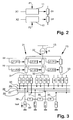
- FIG. 2 represents two resistive elements in series referenced respectively G1 and G2.
- the conductance of each of these resistive elements is controlled by a circuit for evaluating the degree of truth of a condition.
- the two circuits for evaluating the degree of truth, or in other words, the membership function are symbolized by rectangular boxes which are respectively referenced 11 and 13.
- Each of the evaluation circuits is provided for making a comparison between the value of an input signal x k and a value of reference. Depending on the result of this comparison, the evaluation circuit varies the conductance of a resistive element.
- the conductance is expected to be substantially zero when the input value is very different from the reference value, to increase continuously when the two values approach and to reach a maximum when the two values are identical.
- G the conductance equivalent to these two conductances in series.
- An advantage of the present invention is its low consumption. Indeed, in accordance with the present invention, current flows only in the branches of the network of resistive elements which correspond to the rules whose overall degree of truth is not zero.
- a controller according to the present invention can operate at very low voltage.
- Another advantage of the present invention is that the output values associated with the rules being represented in an essentially binary form (the selection or not of an arm), it is possible to produce, for example, easily programmable circuits or circuits specialized by pre-programming the predetermined values in the form of short circuits on one of the conductive masks.
- the controller has six circuits for evaluating a membership function, that is to say a circuit for evaluating a membership function by condition.
- the evaluation circuits are represented by rectangular boxes referenced respectively ⁇ 1 (x1), ⁇ 2 (x1), ⁇ 3 (x1), ⁇ 1 (x2), ⁇ 2 (x2) and ⁇ 3 (x2).
- Each of the evaluation circuits is provided for evaluating the membership function by carrying out a comparison between, on the one hand, an input signal (either x1 or x2) and, on the other hand, a reference value.
- the membership function is zero when the input value is very different from the reference value, increases continuously when the two values come together and reaches a maximum when the two values are identical.
- the controller also comprises a current source referenced 15 connected in series with a formed network.
- resistive elements with variable conductance respectively referenced G11, G21, G31, G12, G22 and G32 (see FIG. 4A).
- the network of resistive elements is formed by three parallel branches, referenced respectively 21, 22 and 23, and which each comprise two resistive elements in series. Each pair of resistive elements in series is associated with the two conditions of a rule.
- Each resistive element is, moreover, intended to be controlled by one of the evaluation circuits of a membership function so that its conductance is zero when the membership function is zero and that its conductance is maximum when the membership function is maximum.
- FIG. 3 The circuit elements of FIG. 3 which have just been described constitute an embodiment of the first means which are claimed by the present invention and which are designed to supply, for each rule, a current representative of the overall degree of truth of said rule.
- FIG. 4A separately takes up the elements of FIG. 3 which constitute the first means above.
- the current source 15 is connected to a node 17 by means of which it supplies current to the three branches 21, 22 and 23 of the network of resistive elements with variable conductance.
- G i the equivalent conductance of branch i (either branch 21, or branch 22, or branch 23)
- the effect on the total conductance of a branch G i of the series connection of two resistive elements is similar to the effect of the fuzzy operator "AND" on two membership functions.
- the distribution of the currents I i between the branches therefore reflects the distribution of the global degrees of truth or, in other words, of the weights between the different rules. This distribution of the weights is however normalized so that the sum of the weights remains constant.
- the fuzzy logic controller further comprises means for determining the value of the output variables from the currents supplied by the resistive network.
- the resistive network of FIG. 4B is intended to implement two rules comprising conditions linked by the term "OR".
- the resistive elements corresponding to the different conditions of the same rule are interconnected so as to form a single resistive bipole or, in other words, a single branch of the network of resistive elements.
- some of the resistive elements associated with the same rule are connected in parallel. Indeed, in the same bipole, the parallel connections correspond to the terms "or" and the serial connections to the terms "and".
- FIGS. 4A and 4B which have just been described respectively represent two resistive networks each comprising a network of resistive bipoles in parallel, the latter network being arranged in series with a current source.
- resistive networks each comprising a network of resistive bipoles in parallel, the latter network being arranged in series with a current source.
- This variant comprises means according to the invention for determining the value of the output variables as a function of the currents supplied by the resistive network.
- each of the branches 21, 22 and 23 of the resistive network is connected to four signal collecting lines referenced 25, 26 27 and 28 respectively and to a ground collector (or "dump" line) referenced 30.
- the connection between each of the branches of the resistive network and the collector lines is made by means of a current divider circuit.
- each of the current dividing circuits comprises four arms of equal conductance which are connected together to one of the outputs of the resistive network.
- the three current dividing circuits are respectively referenced 31, 32 and 33.
- FIG. 5 represents one of the three current dividing circuits of FIG. 3 in isolation and the interconnections of this with the four collector lines 25, 26, 27 and 28 and with the "dump" line 30.
- the current divider circuit of FIG. 5 has four arms, one for each of the collector lines 25, 26, 27 and 28.
- the number of collector lines can be arbitrary but the divider circuits of current always have one arm per collector line.
- each of the four arms of the current divider circuit there is shown a resistive element on each of the four arms of the current divider circuit. These resistive elements are all referenced by the letter G and, moreover, all have the same conductance.
- the current divider circuit divides the current supplied by a branch of the resistive network into four equal parts, provided that the potentials of the collector lines are equal.
- Each arm of the current divider circuit is associated with one of the collector lines but is intended to be connected either to this collector line or to the "dump" line.
- the first arm from the left of the current divider circuit is associated with the collector line 25 to which it is connected
- the second arm is associated with the line 26 but is not connected to it
- the third arm is associated with the line 27 to which it is connected
- the last arm is associated with line 28 but is not connected to it.
- a four-arm current divider circuit is therefore characterized by a four-bit word.
- the four-bit word characterizing the current divider circuit in Figure 5 is 1010.
- the current I i being equal to I o ⁇ G i / i G i the ratio between, on the one hand, the total current supplied to the k th collector line and, on the other hand, the quarter or, more generally, the 1 / N of the total current I0 is therefore equal to the center of gravity of the c k corresponding to the three rules and whose weights are the respective weights of the rules.
- the current supplied to the k th collector line corresponds to the evaluation of the overall output value of three associated rules each having for unique output value one of the values 1 or 0.
- the intensities of the currents in the four lines collectors correspond to the global output values for three associated rules, each having four distinct binary output values.
- the four binary output values which are determined by the connections of the current divider circuit associated with each rule can, according to the present invention, either be considered as four one-bit binary numbers, or as a four-bit binary number, or even like two or three binary numbers of intermediate size.
- each of the collector lines 25, 26, 27 and 28 is, in FIG. 3, connected to one of the inputs 35, 36, 37 and 38 of a second network of resistors.
- This network which constitutes a weighting circuit by powers of 2 known per se, is shown in isolation in FIG. 6.
- the four inputs of the second resistance network each correspond to a node.
- These nodes are respectively referenced 35, 36, 37 and 38.
- the four nodes are interconnected by three resistors all having the same arbitrary value denoted R in the figure, and each of the nodes is also connected to ground via d '' a resistor having either the value R or the value 2R.
- the current supplied by the collector line 25 to the node 38 is indicated by the reference I out, 3
- the current supplied by the line 26 to the node 37 is indicated I out, 2
- the current supplied by line 27 at node 36 is indicated I out, 1
- the current supplied by line 28 at node 35 is indicated I out, 0 .
- I out 2/3 (1/8 I out, 0 + 1/4 I out, 1 + 1/2 I out, 2 + I out, 3 )
- the current Iout is therefore proportional to a sum of the currents supplied to the four collector lines, this sum being weighted by successive powers of 2.
- the effect of the second resistance network is therefore to transform four currents each representing the center of gravity of three binary one-bit numbers into a single current whose intensity represents the center of gravity of three binary four-bit numbers.
- each current divider circuit divides the current it receives into four equal parts. As we have already said, this is only true provided that the four collector lines 25, 26, 27, 28 and the "dump" line 30 are all at the same potential. Unfortunately, since the collector lines are connected to the inputs of the second resistance network and do not conduct the same amount of current, they are generally not exactly at the same potential.
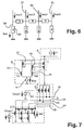
- FIG. 7 represents a second embodiment of a fuzzy logic controller according to the present invention.
- This second embodiment uses MOS transistors in place of the resistive elements of the first embodiment.
- the essential part of the diagram of FIG. 7 is obtained by replacing each of the conductances of the diagram of FIG. 3 with a MOS transistor in accordance with the principle of pseudoresistivity.
- E. Vittoz and X. Arreguit "Linear networks based on transistors", Electronic Letters, 297, 29, (1993)
- circuit in Figure 7 is subdivided into five circuit elements or modules. These modules are respectively referenced A, B, C, D and E and are each delimited by a rectangle in broken lines on the diagram.
- Module A includes the current source.
- This current source can be identical to that of the embodiment of Figure 3. This module is unique, regardless of the number of rules.
- Module B is a circuit for evaluating a membership function or, in other words, a circuit which measures the degree of similarity between the value of an input signal Vx and a given reference value Vp i .
- FIG. 7 represents only a single evaluation circuit of a membership function, but it is clear that there must be one for each condition of each rule implemented.
- the module C is formed of two transistors in series which, when controlled by the module B, together constitute a pseudo-resistive element with variable conductance.
- the conductance of module C is zero if the value of the input signal is very different from the reference value, increases continuously when the two values approach and reaches a maximum value when the two values are identical.
- FIG. 7 represents only one pseudo-resistive element with variable conductance. It is, however, clear that there is one of these elements for each evaluation circuit of a membership function and that, moreover, these pseudo-resistive elements form a network. The reader may refer to Figures 3 and 4 to determine how the pseudo-resistive elements should be interconnected.
- the module D is formed by four collector lines, a "dump" line and a branch circuit whose function is to distribute parts of the current supplied by one of the branches of the network of pseudo-resistive elements to the collector lines.
- the circuit of module D is identical to that of FIG. 5 from the moment when each of the conductances of this latter circuit is replaced by an MOS transistor. It will also be understood that although the module D is represented as comprising only a single branch circuit, it in fact comprises one per rule implemented, ie one per branch of the pseudo-resistive network.
- module E formed by a circuit for carrying out a sum of currents weighted by powers of 2.
- the circuit of module E is identical to the network of resistors of FIG. 6 from the moment when each of the resistors of this network by a MOS transistor (except the two resistors of double value which are replaced by a pair of MOS transistors in series). It will be understood that the module E is also unique regardless of the number of rules.
- the module referenced B is an evaluation circuit of a membership function.
- This module includes a current source referenced 41 which supplies two parallel branches.
- a first of these branches comprises two transistors in series referenced respectively 43 and 47 and the other branch comprises two other transistors referenced respectively 45 and 49.
- the input value for the evaluation circuit is a voltage denoted V x which is supplied to the gate of transistor 43, while the reference value of the circuit is a voltage denoted V pi which is supplied to the gate of transistor 45
- V x which is supplied to the gate of transistor 43
- V pi which is supplied to the gate of transistor 45
- the pseudo-conductance of the transistors of block D is determined by a bias voltage which is denoted Vbias1 and which is delivered by a voltage source referenced 51.
- the pseudo-conductance of the transistors of block E is determined by a bias voltage which is denoted Vbias2 and which is delivered by a voltage source referenced 53.
Landscapes
- Engineering & Computer Science (AREA)
- Software Systems (AREA)
- Theoretical Computer Science (AREA)
- General Physics & Mathematics (AREA)
- Physics & Mathematics (AREA)
- Computational Mathematics (AREA)
- Evolutionary Computation (AREA)
- Molecular Biology (AREA)
- Fuzzy Systems (AREA)
- Biomedical Technology (AREA)
- Algebra (AREA)
- Artificial Intelligence (AREA)
- Health & Medical Sciences (AREA)
- Data Mining & Analysis (AREA)
- General Health & Medical Sciences (AREA)
- Automation & Control Theory (AREA)
- Mathematical Analysis (AREA)
- Mathematical Optimization (AREA)
- Pure & Applied Mathematics (AREA)
- Computing Systems (AREA)
- General Engineering & Computer Science (AREA)
- Mathematical Physics (AREA)
- Life Sciences & Earth Sciences (AREA)
- Feedback Control In General (AREA)
Applications Claiming Priority (2)
| Application Number | Priority Date | Filing Date | Title |
|---|---|---|---|
| FR9411957 | 1994-10-06 | ||
| FR9411957A FR2725539B1 (fr) | 1994-10-06 | 1994-10-06 | Controleur a logique floue de type analogique |
Publications (2)
| Publication Number | Publication Date |
|---|---|
| EP0706143A1 true EP0706143A1 (de) | 1996-04-10 |
| EP0706143B1 EP0706143B1 (de) | 2002-09-11 |
Family
ID=9467630
Family Applications (1)
| Application Number | Title | Priority Date | Filing Date |
|---|---|---|---|
| EP95115575A Expired - Lifetime EP0706143B1 (de) | 1994-10-06 | 1995-10-02 | Analoger Fuzzy-Regler |
Country Status (5)
| Country | Link |
|---|---|
| US (1) | US5712958A (de) |
| EP (1) | EP0706143B1 (de) |
| JP (1) | JPH08297714A (de) |
| DE (1) | DE69528129D1 (de) |
| FR (1) | FR2725539B1 (de) |
Cited By (1)
| Publication number | Priority date | Publication date | Assignee | Title |
|---|---|---|---|---|
| EP0792063A1 (de) * | 1996-02-23 | 1997-08-27 | CSEM Centre Suisse d'Electronique et de Microtechnique S.A. - Recherche et Développement | Feld aus photoempfindlichen Sensoren und daraus aufgebauter Bildsensor |
Families Citing this family (9)
| Publication number | Priority date | Publication date | Assignee | Title |
|---|---|---|---|---|
| US6026372A (en) * | 1997-05-27 | 2000-02-15 | Savage; John K. | Computer system for maintaining current and predicting future food needs |
| FR2770915B1 (fr) * | 1997-11-13 | 2001-11-02 | Schneider Electric Sa | Systeme de programmation d'un automate programmable en logique floue |
| US7124145B2 (en) | 2003-03-27 | 2006-10-17 | Millennium It (Usa) Inc. | System and method for dynamic business logic rule integration |
| US20050216349A1 (en) * | 2004-03-25 | 2005-09-29 | Prince Castle, Inc. | Portable timer system for restaurant inventory management |
| US7132926B2 (en) * | 2004-03-25 | 2006-11-07 | Prince Castle, Inc. | Smart tray system and method for restaurant inventory management |
| DE102004022963A1 (de) * | 2004-05-10 | 2005-12-08 | Ems-Chemie Ag | Thermoplastische Polyamid-Formmassen |
| US8099441B2 (en) | 2004-09-30 | 2012-01-17 | Millennium It (Usa) Inc. | System and method for configurable trading system |
| US10455983B2 (en) | 2015-09-10 | 2019-10-29 | Prince Castle LLC | Modular food holding system |
| US11278157B2 (en) | 2018-03-22 | 2022-03-22 | Marmon Foodservice Technologies, Inc. | Food tray |
Citations (1)
| Publication number | Priority date | Publication date | Assignee | Title |
|---|---|---|---|---|
| JPH05250500A (ja) * | 1992-03-05 | 1993-09-28 | Sharp Corp | ファジィー論理集積回路 |
Family Cites Families (5)
| Publication number | Priority date | Publication date | Assignee | Title |
|---|---|---|---|---|
| US5167005A (en) * | 1988-08-19 | 1992-11-24 | Research Development Corporation Of Japan | Fuzzy computer |
| RU2110826C1 (ru) * | 1989-08-31 | 1998-05-10 | Омрон Корпорейшн | Способ формирования нечеткого управляющего воздействия, устройство для его реализации, способ управления и система для его реализации (варианты) |
| US5412752A (en) * | 1991-06-12 | 1995-05-02 | American Neurologix, Inc. | Expandable fuzzy microcontroller core |
| US5570456A (en) * | 1993-03-26 | 1996-10-29 | Csem Centre Suisse D'electronique Et De Microtechnique Sa - Recherche Et Developpment | Analog circuit implementing a fuzzy logic controller |
| US5572626A (en) * | 1994-05-19 | 1996-11-05 | Lin; Hung C. | Fuzzy membership function generator using resonant tunneling diodes |
-
1994
- 1994-10-06 FR FR9411957A patent/FR2725539B1/fr not_active Expired - Fee Related
-
1995
- 1995-09-22 US US08/532,875 patent/US5712958A/en not_active Expired - Fee Related
- 1995-10-02 DE DE69528129T patent/DE69528129D1/de not_active Expired - Lifetime
- 1995-10-02 EP EP95115575A patent/EP0706143B1/de not_active Expired - Lifetime
- 1995-10-06 JP JP7284347A patent/JPH08297714A/ja active Pending
Patent Citations (1)
| Publication number | Priority date | Publication date | Assignee | Title |
|---|---|---|---|---|
| JPH05250500A (ja) * | 1992-03-05 | 1993-09-28 | Sharp Corp | ファジィー論理集積回路 |
Non-Patent Citations (3)
| Title |
|---|
| E. VITTOZ ET X. ARREGUIT: "Linear networks based on transistors", ELECTRONIC LETTERS, vol. 287, 1993, pages 29 |
| PATENT ABSTRACTS OF JAPAN vol. 018, no. 014 (P - 1672) 11 January 1994 (1994-01-11) * |
| SASAKI M ET AL: "A fuzzy logic function generator (FLUG) implemented with current mode CMOS circuits", PROCEEDINGS OF THE TWENTY-FIRST INTERNATIONAL SYMPOSIUM ON MULTIPLE-VALUED LOGIC (CAT. NO.91CH3009-8), VICTORIA, BC, CANADA, 26-29 MAY 1991, ISBN 0-8186-2145-1, 1991, LOS ALAMITOS, CA, USA, IEEE COMPUT. SOC. PRESS, USA, pages 356 - 362 * |
Cited By (1)
| Publication number | Priority date | Publication date | Assignee | Title |
|---|---|---|---|---|
| EP0792063A1 (de) * | 1996-02-23 | 1997-08-27 | CSEM Centre Suisse d'Electronique et de Microtechnique S.A. - Recherche et Développement | Feld aus photoempfindlichen Sensoren und daraus aufgebauter Bildsensor |
Also Published As
| Publication number | Publication date |
|---|---|
| DE69528129D1 (de) | 2002-10-17 |
| US5712958A (en) | 1998-01-27 |
| JPH08297714A (ja) | 1996-11-12 |
| FR2725539A1 (fr) | 1996-04-12 |
| FR2725539B1 (fr) | 1996-11-29 |
| EP0706143B1 (de) | 2002-09-11 |
Similar Documents
| Publication | Publication Date | Title |
|---|---|---|
| EP0706143B1 (de) | Analoger Fuzzy-Regler | |
| EP2602937B1 (de) | Digital-Analog-Wandler und neuromorpher Schaltkreis, bei dem dieser Wandler eingesetzt wird | |
| EP0387146B1 (de) | Analoges programmierbares neuronales Netzwerk | |
| EP0733961A1 (de) | Referenzstromgenerator in CMOS-Technologie | |
| FR2689706A1 (fr) | Convertisseur numérique-analogique comportant un tampon de sortie à tension de décalage ajustable. | |
| WO2019219618A1 (fr) | Synapse artificielle commutee | |
| US20200380349A1 (en) | Auto Weight Scaling for RPUs | |
| EP0901227A1 (de) | Schaltung mit variabler Verzögerung | |
| JP2017049945A (ja) | 信号発生装置および伝送装置 | |
| EP0568145A1 (de) | Neuronalprozessor mit Norm- oder Distanzrechnungsmittel | |
| FR2665969A1 (fr) | Reseau neural a couches multiples et son procede de conception. | |
| EP0621549B1 (de) | Einheit mit nichtlinearer Betriebsweise und auf einer Einheit mit nichtlinearer Betriebsweise basierte Datenverarbeitungsanlage | |
| BE1005270A5 (fr) | Dispositif mosfet de controle de multiplicateur. | |
| EP0283393A1 (de) | Binäre Rechnungseinrichtung | |
| FR2699307A1 (fr) | Procédé et dispositif pour la convolution analogique d'images. | |
| EP0938732B1 (de) | Analoge elektrische zelle, insbesondere zur implantierung in einen integrierten schaltkreis und integrierter schaltkreis damit | |
| Halawani et al. | A re-configurable memristor array structure for in-memory computing applications | |
| EP0543730B1 (de) | Neuronaler Analog-/Digitalwandler | |
| EP0777322A1 (de) | Spannungsverstärker mit grossen dynamischen Bereich und A/D-Konverter damit | |
| EP1131890B1 (de) | Digital/analogwandler | |
| EP1066557B1 (de) | Schneller verkettenbarer volladdierer mit differentiellen eingängen | |
| EP4354351B1 (de) | Elektronische schaltung auf rram-zellenbasis | |
| FR2681710A1 (fr) | Calculateur neuronal. | |
| FR2713369A1 (fr) | Contrôleur à logique floue. | |
| EP0917288A1 (de) | Zelle mit Pseudo-Kapazität, insbesondere für künstliche Netzhaut |
Legal Events
| Date | Code | Title | Description |
|---|---|---|---|
| PUAI | Public reference made under article 153(3) epc to a published international application that has entered the european phase |
Free format text: ORIGINAL CODE: 0009012 |
|
| AK | Designated contracting states |
Kind code of ref document: A1 Designated state(s): DE FR GB NL |
|
| 17P | Request for examination filed |
Effective date: 19961010 |
|
| 17Q | First examination report despatched |
Effective date: 20000714 |
|
| GRAG | Despatch of communication of intention to grant |
Free format text: ORIGINAL CODE: EPIDOS AGRA |
|
| GRAG | Despatch of communication of intention to grant |
Free format text: ORIGINAL CODE: EPIDOS AGRA |
|
| GRAH | Despatch of communication of intention to grant a patent |
Free format text: ORIGINAL CODE: EPIDOS IGRA |
|
| GRAH | Despatch of communication of intention to grant a patent |
Free format text: ORIGINAL CODE: EPIDOS IGRA |
|
| GRAH | Despatch of communication of intention to grant a patent |
Free format text: ORIGINAL CODE: EPIDOS IGRA |
|
| GRAA | (expected) grant |
Free format text: ORIGINAL CODE: 0009210 |
|
| AK | Designated contracting states |
Kind code of ref document: B1 Designated state(s): DE FR GB NL |
|
| PG25 | Lapsed in a contracting state [announced via postgrant information from national office to epo] |
Ref country code: NL Free format text: LAPSE BECAUSE OF FAILURE TO SUBMIT A TRANSLATION OF THE DESCRIPTION OR TO PAY THE FEE WITHIN THE PRESCRIBED TIME-LIMIT Effective date: 20020911 |
|
| REG | Reference to a national code |
Ref country code: GB Ref legal event code: FG4D Free format text: NOT ENGLISH |
|
| REF | Corresponds to: |
Ref document number: 69528129 Country of ref document: DE Date of ref document: 20021017 |
|
| PG25 | Lapsed in a contracting state [announced via postgrant information from national office to epo] |
Ref country code: DE Free format text: LAPSE BECAUSE OF FAILURE TO SUBMIT A TRANSLATION OF THE DESCRIPTION OR TO PAY THE FEE WITHIN THE PRESCRIBED TIME-LIMIT Effective date: 20021212 |
|
| GBT | Gb: translation of ep patent filed (gb section 77(6)(a)/1977) |
Effective date: 20030107 |
|
| NLV1 | Nl: lapsed or annulled due to failure to fulfill the requirements of art. 29p and 29m of the patents act | ||
| PLBE | No opposition filed within time limit |
Free format text: ORIGINAL CODE: 0009261 |
|
| 26N | No opposition filed |
Effective date: 20030612 |
|
| REG | Reference to a national code |
Ref country code: FR Ref legal event code: TP |
|
| REG | Reference to a national code |
Ref country code: GB Ref legal event code: 732E |
|
| PGFP | Annual fee paid to national office [announced via postgrant information from national office to epo] |
Ref country code: GB Payment date: 20070925 Year of fee payment: 13 |
|
| PGFP | Annual fee paid to national office [announced via postgrant information from national office to epo] |
Ref country code: FR Payment date: 20071030 Year of fee payment: 13 |
|
| GBPC | Gb: european patent ceased through non-payment of renewal fee |
Effective date: 20081002 |
|
| REG | Reference to a national code |
Ref country code: FR Ref legal event code: ST Effective date: 20090630 |
|
| PG25 | Lapsed in a contracting state [announced via postgrant information from national office to epo] |
Ref country code: FR Free format text: LAPSE BECAUSE OF NON-PAYMENT OF DUE FEES Effective date: 20081031 |
|
| PG25 | Lapsed in a contracting state [announced via postgrant information from national office to epo] |
Ref country code: GB Free format text: LAPSE BECAUSE OF NON-PAYMENT OF DUE FEES Effective date: 20081002 |