EP0283393A1 - Binäre Rechnungseinrichtung - Google Patents
Binäre Rechnungseinrichtung Download PDFInfo
- Publication number
- EP0283393A1 EP0283393A1 EP88400589A EP88400589A EP0283393A1 EP 0283393 A1 EP0283393 A1 EP 0283393A1 EP 88400589 A EP88400589 A EP 88400589A EP 88400589 A EP88400589 A EP 88400589A EP 0283393 A1 EP0283393 A1 EP 0283393A1
- Authority
- EP
- European Patent Office
- Prior art keywords
- transistors
- signal
- bits
- input
- exclusive
- Prior art date
- Legal status (The legal status is an assumption and is not a legal conclusion. Google has not performed a legal analysis and makes no representation as to the accuracy of the status listed.)
- Ceased
Links
Images





Classifications
-
- G—PHYSICS
- G06—COMPUTING OR CALCULATING; COUNTING
- G06F—ELECTRIC DIGITAL DATA PROCESSING
- G06F7/00—Methods or arrangements for processing data by operating upon the order or content of the data handled
- G06F7/38—Methods or arrangements for performing computations using exclusively denominational number representation, e.g. using binary, ternary, decimal representation
- G06F7/48—Methods or arrangements for performing computations using exclusively denominational number representation, e.g. using binary, ternary, decimal representation using non-contact-making devices, e.g. tube, solid state device; using unspecified devices
- G06F7/50—Adding; Subtracting
- G06F7/504—Adding; Subtracting in bit-serial fashion, i.e. having a single digit-handling circuit treating all denominations after each other
-
- G—PHYSICS
- G06—COMPUTING OR CALCULATING; COUNTING
- G06F—ELECTRIC DIGITAL DATA PROCESSING
- G06F7/00—Methods or arrangements for processing data by operating upon the order or content of the data handled
- G06F7/38—Methods or arrangements for performing computations using exclusively denominational number representation, e.g. using binary, ternary, decimal representation
- G06F7/48—Methods or arrangements for performing computations using exclusively denominational number representation, e.g. using binary, ternary, decimal representation using non-contact-making devices, e.g. tube, solid state device; using unspecified devices
- G06F7/50—Adding; Subtracting
- G06F7/501—Half or full adders, i.e. basic adder cells for one denomination
-
- G—PHYSICS
- G06—COMPUTING OR CALCULATING; COUNTING
- G06F—ELECTRIC DIGITAL DATA PROCESSING
- G06F7/00—Methods or arrangements for processing data by operating upon the order or content of the data handled
- G06F7/38—Methods or arrangements for performing computations using exclusively denominational number representation, e.g. using binary, ternary, decimal representation
- G06F7/48—Methods or arrangements for performing computations using exclusively denominational number representation, e.g. using binary, ternary, decimal representation using non-contact-making devices, e.g. tube, solid state device; using unspecified devices
- G06F7/50—Adding; Subtracting
- G06F7/501—Half or full adders, i.e. basic adder cells for one denomination
- G06F7/503—Half or full adders, i.e. basic adder cells for one denomination using carry switching, i.e. the incoming carry being connected directly, or only via an inverter, to the carry output under control of a carry propagate signal
Definitions
- the present invention relates to a binary calculation device and more precisely a device for calculating the sum and / or the difference of binary digits or bits. It finds an application in the realization of binary electronic systems such as adders, multipliers, dividers, accumulators ... etc.
- the elementary cell of these devices is the addition cell or adder.
- the adder includes a first bit input (A i ), a second bit input (B i ) and an upstream carry input (R i-1 S).
- the adder produces a result signal (S i ) and a downstream transfer signal (R i S) using four reversing gates I1, I2, ..., two exclusive OR gates XOR1, XOR2 and four transmission gates C1, C2, ...
- the inverter gates I change the logic state of the signal applied to the input of said gates.
- the exclusive OR gate XOR1 calculates the exclusive OR signal of the two input bits (A i ⁇ B i ) and the exclusive OR gate XOR2 calculates the signal Exclusive OR complemented by the two input bits ( A i ⁇ B i ).
- the transmission gates C1 and C2 calculate the downstream carry signal (R i S) and the transmission gates C3 and C4 calculate the resulting signal (S i ).
- the different gates consist of one or more pairs of transistors T in complementary MOS technology, that is to say of opposite polarities. The transistors are arranged according to the logical property of the door.
- the adder thus comprises 24 transistors.
- This adder is not satisfactory because it includes a large number of transistors.
- the object of the invention is precisely to reduce the number of transistors of a complete adder. To this end, it offers an addition cell using in its most reduced version only 15 transistors.
- This object is achieved by using only an exclusive OR gate (XOR) calculating the exclusive OR signal of the two input bits (A i ⁇ B i ) and by reversing this signal to produce the exclusive OR signal complemented by the two bits (( A i ⁇ B i ).
- XOR exclusive OR gate
- the invention relates to a binary calculation device, of the type comprising at least one cell having: - an entry of the first binary digits or bits (A i ), - an input of second bits (B i ), - an upstream carry-over input (R i-1 ), - first means for generating an exclusive OR signal of the two input bits (A i ⁇ B i ) and its complement ( A i ⁇ B i ), - second means for producing a result signal by an exclusive OR function of the upstream transfer (R i-1 ) with the exclusive OR signal of the two bits (A i ⁇ B i ) and its complement ( A i ⁇ B i ), - third means for producing a downstream carry signal (R i ) by a transmission function comprising two transmission gates controlled by the exclusive OR signal of the two input bits (A i ⁇ B i ) and its complement ( A i ⁇ B i ), one of the gates allowing the passage of the upstream carry signal (R i-1
- the exclusive OR signal complemented by the two bits ( A i ⁇ B i ) is produced by the inversion of the signal (A i ⁇ B i ).
- the first means comprise a first pair of transistors of opposite polarities, the gate of each of the transistors being connected to the input of the first bit (A i ), a positive electric voltage being applied to the drain of one of the transistors, the mass being applied to the source of the other transistor, the source of one of the transistors and the drain of the other transistor being connected to a first node;
- the first means also comprise a second pair of transistors of opposite polarities, the drain of one of the transistors being connected to the input of the first bit (A i ) and the source of the other transistor being connected to the first node, the gate of each of the two transistors being connected to the input of the second bit (B i ), the source of one of the transistors and the drain of the other transistor being connected to a second node and the first means finally comprise a third pair of transistors of opposite polarities, the source of each of the two transistors being connected to the second node, the drain of each of the two transistors being
- the first means further comprise a pair of transistors of opposite polarities, the gate of each of the transistors being connected to the exclusive OR signal of the two input bits, a positive electric voltage being applied to the drain of one of the transistors, the mass being applied to the source of the other transistor, the exclusive OR signal complemented by the two input bits ( A i ⁇ B i ) being obtained at the node connecting the source of one of the transistors to the drain of the other transistor.
- the first means comprise a first pair of transistors of the same polarity, the gate of one of the transistors being connected to the input of first bits (A i ), the gate of the other of the transistors being connected to the input of the second bits (B i ), an electric voltage being applied to the drain of one of the transistors, the source of one of the transistors being connected to the drain of the other of the transistors, the source of the other of the transistors being connected to a third node
- the first means also comprise a second pair of transistors of polarities opposite to those of the transistors of the first pair, the drain of one of the transistors being connected to the input of the first bits (A i ), the gate of one of the transistors being connected to the input of the second bits (B i ), the drain of the other of the transistors being connected to the input of second bits (B i ), the gate of the other of the transistors being connected to the ent rée of first bits (A i ), the source
- the first means further comprise a pair of transistors of opposite polarities, the gate of each of the transistors being connected to the exclusive OR signal complemented by the two input bits ( A i ⁇ B i ), an electric voltage being applied to the drain of one of the transistors, the mass being applied to the source of the other of the transistors, the exclusive OR signal of the two input bits (A i ⁇ B i ) being obtained to the node connecting the source of one of the transistors to the drain of the other transistor.
- the second means calculate the modulo sum of the first bit (A i ), second bit (B i ) and upstream carry (R i-1 ).
- the second means calculate the complement of the modulo sum of the first bit (A i ) of the second bit (B i ) and the upstream carry-over (R i-1 ).
- the third means calculate the sum of the product of the two bits, the product of one of the two bits (A i , B i ) by the carry (R i-1 ) and the product of the other of the two bits (A i , B i ) by the upstream carry-over (R i-1 ).
- the second means comprise two pairs of transistors of opposite polarities, in one of the two pairs the gate of each of the transistors being connected to the upstream transfer input (R i-1 ), the drain of one of the transistors being connected to the exclusive OR signal of the two input bits (A i ⁇ B i ), the source of the other transistor being connected to the complement of the exclusive OR signal of the two input bits ( A i ⁇ B i ), a result signal being obtained at a fourth node connecting the source of one of the transistors to the drain of the other transistor, in the other of the two pairs, the drain of each of the transistors being connected to the upstream transfer (R i-1 ), the gate of one of the transistors being connected to the exclusive OR signal of the two input bits (A i ⁇ B i ) and the gate of the other of the transistors being connected to the complement of the OR signal exclusive of the two input bits ( A i ⁇ B i ), the result signal being obtained at the fourth node
- the third means comprise two pairs of transistors of opposite polarities, in one: the gate of one of the transistors being connected to the exclusive OR signal of the two bits input (A i ⁇ B i ) and the gate of the other transistor being connected to the complement of the exclusive OR signal of the two input bits ( A i ⁇ B i ), the drain of each of the transistors being connected to the upstream transfer (R i-1 ), the downstream transfer signal (R i ) being obtained at a fifth node connecting the source of each of the transistors, in the other of the two pairs : the gate of one of the transistors being connected to the exclusive OR signal of the two input bits (A i ⁇ B i ) and the gate of the other transistor being connected to the complement of the exclusive OR signal of the two bits d 'Entrance ( A i ⁇ B i ), the source of each of the transistors being connected to the first input bit (A i ), the downstream transfer signal (R i ) being
- the invention also relates to a device with several cells in parallel arranged as an adder module, with spread report.
- the first cell of two adjacent cells comprises an upstream transfer (R i-1 ) and a complemented downstream transfer ( R i ) and the second cell of the two adjacent cells includes a complemented upstream transfer ( R i ) and a downstream carry-over (R i-1 ).
- the complement ( R i ) of the downstream carry signal of the first cell of two adjacent cells and the complement ( R i ) of the upstream transfer signal of the second cell of the two adjacent cells are obtained respectively by a pair of transistors of opposite polarities, the gate of each of the transistors being connected to the downstream transfer signal (R i ) of the first cell, respectively at upstream transfer signal (R i ) from the second cell, an electric voltage being applied to the drain of one of the transistors, the mass being applied to the source of the other transistor, the downstream transfer signal complemented ( R i ) of the first cell and the complemented carry-over signal ( R i ) of the second cell being respectively obtained at the node connecting the source of one of the transistors to the drain of the other transistor.
- the invention also relates to a device for calculating binary words of n bits, in which the bits appear sequentially in series at the inputs of the cell.
- the cell also comprises fourth means for memorizing the downstream retention (R i ).
- the fourth means are flip-flops of type D, the downstream reservoir (R i ) being connected to the inlet of the scale and the upstream reservoir (R i-1 ) being connected to the scale output.
- the invention also relates to a device making it possible to calculate simultaneously the sum (S i ) and the difference (D i ) of the input bits.
- the device comprises an addition cell calculating the sum (S i ) of the input bits and a subtraction cell calculating the difference (D i ) of the bits of input, the first means producing the exclusive OR signal (A i ⁇ B i ) and its complement being used in common by the addition and subtraction cells.
- the device is arranged in adder-subtractor modules with propagated transfer.
- the device is arranged in adder-subtractor modules in which the input bits appear sequentially in series at the inputs of the cells.
- the invention also relates to a device with several cells in parallel.
- the device is arranged in add-on and / or subtractor modules with early carry-over.
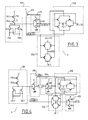
- FIG. 2 schematically illustrates a full adder with three inputs on one bit comprising 16 transistors, in accordance with the invention.
- the adder 2 includes a first bit input (A i ), a second bit input (B i ) and an upstream carry input (R i-1 S).
- the adder 2 produces a result signal (S i ).
- the result is the sum of the two bits (A i , B i ). It is obtained by calculating the modulo sum, also called exclusive OR sum, of the first bits (A i ), of the second bit (B i ) and of the upstream transfer (R i-1 S).
- the adder 2 produces a downstream carry signal (R i S) associated with the result of the calculation of the sum (S i ) of the three input bits (A i ), (B i ) and (R i-1 S) .
- the downstream carry-over signal (R i S) is obtained by calculating the sum of the product of the two bits, of the product of one of the bits by the upstream carry-over (R i-1 S) and of the product of the other of the two bits by the upstream transfer (R i-1 S).
- the adder 2 firstly comprises first means 100 for generating an exclusive OR signal from the two input bits (A i ⁇ B i ).
- These first means 100 comprise a pair of transistors 101 and 102 complementary to MOS technology.
- the transistor 101 is on the P channel and the transistor 102 is on the N channel.
- the gate G of each of the transistors 101 and 102 is connected to the first bit input (A i ).
- An electric voltage V is applied to the drain D of the transistor 101.
- V has a value of 5 volts for example, in the case of transistors in MOS technology.
- Ground is applied to the source S of transistor 102.
- the source of transistor 101 and the drain of transistor 102 are connected to a first node 103.
- the first means 100 also comprise a second pair of transistors 104 and 105 complementary to MOS technology.
- the transistor 104 is on the P channel and the transistor 105 is on the N channel.
- the drain of the transistor 104 is connected to the input of first bits (A i ) and the source of the transistor 105 is connected to the first node 103.
- the gate of each of the transistors 104 and 105 is connected to the input of second bits (B i ).
- the source of transistor 104 and the drain of transistor 105 are connected to a second node 106.
- the first means 100 finally comprise a third pair of complementary transistors 107 and 108.
- the transistor 107 is on the P channel and the transistor 108 is on the N channel.
- the source of transistors 107 and 108 is connected to the second node 106.
- the drain of transistors 107 and 108 is connected to the input of second bits (B i ).
- the gate of transistor 107 is connected to the input of first bits (A i ) and the gate of transistor 108 is connected to the first node 103.
- the exclusive OR signal of the two input bits (A i ⁇ B i ) is obtained at node 106.
- the first means 100 operate as follows:
- the transistor 101 When the first bit signal (A i ) is a positive electric voltage V which corresponds to the high logic state, the transistor 101 is blocked while the transistor 102 is on. In this configuration, a zero voltage which corresponds to the low logic state is obtained at node 103.
- the transistor 101 When the first bit signal (A i ) is a zero voltage, the transistor 101 is on while the transistor 102 is blocked. In this case, a positive electric voltage is obtained at node 103.
- the pair of transistors 101 and 102 plays the role of inverter of the first bit input signal (A i ).
- the complemented signal ( A i ) When the first bit signal (A i ) is in the logic high state, the complemented signal ( A i ) is in the logical low state.
- the pair of transistors 104 and 105 also plays the role of inverter, thus showing the complemented signal ( B i ) at the second node 106.
- the transmission door constituted by the pair of transistors 107 and 108 is open.
- the complemented signal ( A i ) is in the high logical state.
- the transmission door constituted by the pair of transistors 107 and 108 is now closed, making thus pass the signal (B i ) to node 106.
- the pair of transistors 104 and 105 is inactive. We thus obtain at node 106 the exclusive OR signal of the two bits (A i ⁇ B i ).
- the adder then comprises a pair 400 consisting of transistors of opposite polarities.
- This pair 400 receives the exclusive OR signal from the two input bits (A i ⁇ B i ) delivered by the first means 100 to produce the inversion of this signal.
- the first extended means 100 of the pair 400 constitute a module delivering the signal (A i ⁇ B i ) and its complement ( A i ⁇ B i ).
- the pair 400 of transistors consists of a P channel transistor 401 and an N channel transistor 402. The gate of each of the transistors 401 and 402 is connected to the exclusive OR signal of the two input bits (A i ⁇ B i ). An electrical voltage V is applied to the drain of transistor 401.
- V has a value of 5 volts for example in the case of transistors in MOS technology.
- Ground is applied to the source of transistor 402.
- the exclusive OR signal complemented by the two input bits ( A i ⁇ B i ) is obtained at node 403 connecting the source of transistor 401 to the drain of transistor 402.
- the pair of transistors 401 and 402 has the same operation as the pair of transistors 101 and 102 described above.
- the adder 2 then comprises second means 200 for producing a result signal (S i ) by an exclusive OR function of the upstream transfer (R i-1 S) with the exclusive OR signal of the two bits (A i ⁇ B i ) and its complement ( A i ⁇ B i ).
- These second means 200 comprise two pairs of transistors of opposite polarities.
- the first pair consists of transistors 201 and 202.
- Transistor 201 is P-channel and transistor 202 is N-channel.
- the gate of each of transistors 201 and 202 is connected to the upstream transfer input (R i-1 S).
- the drain of transistor 201 is connected to the exclusive OR signal of the two input bits ( A i ⁇ B i ).
- the source of transistor 202 is connected to the exclusive OR signal complement of the two input bits (A i ⁇ B i ).
- the result signal (S i ) is obtained at a node 203 connecting the source of transistor 201 to drain of transistor 202.
- the second pair consists of transistors 204 and 205.
- the transistor 204 is on the P channel and the transistor 205 is on the N channel.
- the drain of each of the transistors 204 and 205 is connected to the upstream transfer (R i-1 S).
- the gate of transistor 204 is connected to the exclusive OR signal of the two input bits (A i ⁇ B i ).
- the gate of transistor 205 is connected to the exclusive OR signal complemented by the two input bits ( A i ⁇ B i ).
- the result signal (S i ) being obtained at node 203 connecting the source of each of the transistors 204 and 205.
- the second means 200 operate as follows:
- the complemented signal ( A i ⁇ B i ) is in the low logic state.
- the pair of transistors 201 and 202 acts as an inverter, causing the complemented signal to appear ( R i-1 S ) at node 203.
- the transmission door constituted by the pair of transistors 204 and 205 is open.
- the adder finally comprises third means 300 for producing a downstream transfer signal (R i S) by a transmission function comprising two transmission gates controlled by the exclusive OR signal of the two input bits (A i ⁇ B i ) and its complement, one of the gates allowing the passage of the upstream transfer signal (R i-1 S) and the other of the gates allowing the passage of one of the two signals of the input bits (A i , B i ).
- the third means 300 comprise two pairs of transistors of opposite polarities.
- the first pair consists of transistors 301 and 302.
- Transistor 301 is N-channel and transistor 302 is P-channel.
- the gate of transistor 301 is connected to the exclusive OR signal of the two bits (A i ⁇ B i ).
- the gate of transistor 302 is connected to the complement of the exclusive OR signal of the two bits ( A i ⁇ B i ).
- the drain of transistors 301 and 302 is connected to the upstream transfer (R i-1 S).
- the downstream transfer signal (R i S) is obtained at node 303 connecting the source of transistors 301 and 302.
- the second pair consists of transistors 304 and 305.
- Transistor 304 is P-channel and transistor 305 is N-channel .
- the gate of transistor 304 is connected to the exclusive OR signal of the two bits (A i ⁇ B i ).
- the gate of transistor 305 is connected to the complement of the exclusive OR signal of the two bits ( A i ⁇ B i ).
- the source of each of the transistors 304 and 305 is connected to the first input bit (A i ).
- the downstream transfer signal (R i S) is obtained at node 303 connecting the drain of each of the transistors 304 and 305.
- the third means (300) operate as follows:
- the exclusive OR signal of the two input bits (A i ⁇ B i ) When the exclusive OR signal of the two input bits (A i ⁇ B i ) is in the high logic state, the complemented signal ( A i ⁇ B i ) is low.
- the transmission door constituted by the transistors 301 and 302 is closed causing the signal (R i-1 S) to appear at node 303.
- the transmission door constituted by the pair of transistors 304 and 305 is inactive.
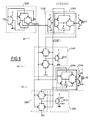
- FIG. 3 schematically illustrates a complete adder with three inputs on one bit comprising 15 transistors according to the invention.
- the first means 100 of the adder 2 described with reference to FIG. 2 are modified.
- the other means 250, 350 and the pair 450 of the adder 4 are identical respectively to the means 200 , 300 and 400 of the adder 2 described with reference to FIG. 2.
- the first means 109 of the adder 4 comprise a pair of P-channel transistors 110 and 111.
- the gate of transistor 110 is connected to the input of first bits (A i ) and the gate of transistor 111 is connected to input of second bits (B i ).
- An electric voltage V is applied to the drain of transistor 110.
- V has a value of 5 volts for example in the case of transistors in MOS technology.
- the source of transistor 110 is connected to the drain of transistor 111.
- the source of transistor 111 is connected to a node 112.
- the first means 109 of the adder 4 also include a pair of transistors consisting of an N-channel transistor 113 and an N-channel transistor 114.
- the drain of transistor 113 is connected to the input of first bits (A i ).
- the gate of transistor 113 is connected to the input of second bits (B i ).
- the drain of transistor 114 is connected to the input of second bits (B i ).
- the gate of transistor 114 is connected to the input of first bits (A i ).
- the exclusive OR signal, complemented by the two input bits ( A i ⁇ B i ) is obtained at node 112 connecting the source of each of transistors 113 and 114.
- the first means 109 of the adder 4 finally comprise a P-channel transistor 115.
- the source of the transistor 115 is connected to node 112.
- An electrical voltage V is applied to the drain of transistor 115.
- the gate of transistor 115 is connected to node 453 of pair 450 made up of transistors 451 and 452.
- transistor 115 The role of transistor 115 is as follows.
- N-type transistor conducts a low logic level applied to its source to its drain when its gate is brought to high logic level while it leads with a loss of signal a high logic level applied to its source to its drain when its grid is brought to the high logic level.
- one aspect of the invention resides in the following arrangements.
- the first means form a first operator with two inputs and an output to produce the signal (A i ⁇ B i ) from the two input bits (A i , B i ), said first operator has furthermore at least one additional output delivering one of the complemented signals ( A i ), ( B i ), ( A i ⁇ B i ).
- the second means form a second operator with two inputs and one output to produce a result signal from the upstream carry-over signal (R i -1) or its complement ( R i -1 ) and of the signal (A i ⁇ B i ) or its complement ( A i ⁇ B i ) delivered by the first means, said second operator also has at least one additional output delivering one of these input signals.
- the Applicants have noticed in particular that the additional output defined by the node 112 of the means 109 can bring the signal ( A i ⁇ B i ) to the third means 350.
- the additional output defined by the node 453 from which the signal leaves (A i ⁇ B i ) to one of the inputs of the second means 250 can bring the signal (A i ⁇ B i ) third pleas 350.
- Another characteristic of the invention is also to use additional outputs provided in the first and second means and capable of bringing the necessary signals to the calculation of the downstream carryover (R i ). This characteristic will also be present in the binary calculation devices described below.
- the invention also relates to a device with several cells in parallel, arranged as a propagated transfer adder module.
- the simple juxtaposition of n adders described with reference to Figures 2 and 3 is not suitable because a set of transistors are connected together in series, forming a linear chain whose equivalent scheme is a network of RC cells.
- the delay F between the output signal and that of the input into such a device is very high.
- a first variant of the device of the invention has just The object is to remedy this drawback.
- FIG. 4 illustrates this first variant and which represents a schematic view of a complete adder 6 with three inputs on one bit, with propagated carryover comprising 18 transistors according to the invention.
- the adder 6 is obtained by modifying the adder 4 described with reference to FIG. 3, by adding to the input of the upstream transfer (R i-1 S) a pair 500 consisting of a transistor 501 with channel P and d an N channel transistor 502, and by adding to the downstream carry signal (R i S) a pair 600 consisting of a P channel transistor 601 and an N channel transistor 602.
- the transistors 501 and 502 of the pair 500 and the transistors 601 and 602 of the pair 600 are arranged so as to reverse respectively the upstream carry signal (R i-1 S) and the downstream carry signal (R i S) as did the transistors 451 and 452 of the pair 450 described with reference to FIG. 3 for the exclusive OR signal complemented by the two input bits ( A i ⁇ B i ).
- the transistor 115 of the first means 109 of the adder 4 described with reference to FIG. 3 has disappeared in the first means 130 of the adder 6 described with reference to FIG. 4 because its role is now held by the pairs 500 and 600 .
- the other means 260, 360 and 460 of the adder 6 are identical respectively to the means 250, 350 and 450 of the adder 4 described with reference to FIG. 3.
- the upstream transfer (R i-1 S) and the downstream transfer (R i S) are complemented respectively by the pair 500 and the pair 600.
- the complementation of the deferrals is used to reduce the propagation time of the deferral in a device with several adders.
- the first adder of two adjacent adders of such a device comprises an upstream transfer (R i-1 S) and a complemented downstream transfer ( R i S ).
- the second adder of the two adjacent adders includes an upstream carry ( R i S ) supplemented and a downstream carry-over (R i + 1 S).
- FIG. 5 schematically represents a complete adder on two bits with propagated transfer comprising 34 transistors according to the invention.
- the adder 8 comprises an adder 10 like that described with reference to FIG. 2 and an adder 12 like that described with reference to FIG. 4.
- the means 140, 470, 270 and 370 of the adder 10 are identical respectively to the means 100, 400, 200 and 300 of the adder 2 described with reference to FIG. 2.
- the upstream transfer (R i-1 S) of the adder 10 is supplemented by a pair 700 of transistors 701 and 702 arranged in the same way as the transistors 401 and 402 of the pair 400 described with reference to FIG. 2.
- the means 150, 480, 280 and 380 are identical respectively to the means 130, 460, 260 and 360 of the adder 6 described with reference to FIG. 4.
- the upstream transfer (R i S) of the adder 12 is obtained by complementing the downstream transfer (R i S) of the adder 10 by a pair 800 consisting of transistors 801 and 802 arranged in the same way as those of the pair 700.
- the adder 8 allows an improvement in the delay of propagation of the delay by a delay corresponding to half the delay of propagation of the delay in a pair 700 compared to an adder made up of two juxtaposed adders described with reference to FIG. 4.
- FIG. 6 schematically represents a complete adder-subtractor with four inputs (A i ), (B i ), (R i-1 S) and (R i-1 D) on a bit comprising 24 transistors , in accordance with the invention.
- the adder-subtractor 14 consists of an adder 16 and a subtractor 18.
- the adder 16 is identical to that described with reference to FIG. 2. It includes a module 1000 calculating the exclusive OR signal (A i ⁇ B i ).
- the module 1000 consists of transistors arranged in the same way as those of the first means 100 described with reference to FIG. 2.
- the adder 16 also comprises a module 1100 calculating the sum (S i ) of the three input bits (A i , B i and R i-1 S).
- the module 1100 consists of transistors arranged in the same way as those of the second means 200 described with reference to FIG. 2.
- the adder 16 also includes a module 1200 calculating the downstream carryover (R i S) associated with the sum of the three bits d 'input (A i , B i and R i-1 S).
- the module 1200 consists of transistors arranged in the same way as those of the third means 300 described with reference to FIG. 2.
- the adder 16 finally comprises a pair 1300 of transistors inverting the exclusive OR signal of the two input bits (A i ⁇ B i ).
- the pair 1300 consists of two transistors arranged in the same way as those of the pair 400 described with reference to FIG. 2.
- the subtractor 18 comprises a module 1400 calculating the difference (D i ) of the two input bits (A i , B i ) taking into account the upstream carry (R i-1 D) and a module 1500 calculating the downstream carry ( R i D) associated with the difference of the two input bits (A i , B i ).
- the 1400 module includes two pairs of transistors of opposite polarities.
- the first pair is made up of transistors 1401 and 1402.
- Transistor 1401 is P-channel and transistor 1402 is N-channel.
- the gate of each of transistors 1401, 1402 is connected to the upstream transfer input (R i-1 D) associated with the difference of the two input bits (A i , B i ).
- the drain of transistor 1401 is connected to the exclusive OR signal complemented by the two input bits ( A i ⁇ B i ).
- the source of transistor 1402 is connected to the exclusive OR signal of the two input bits (A i ⁇ B i ).
- the result signal (D i ) is obtained at a node 1403 connecting the source of transistor 1401 to the drain of transistor 1402.
- the second pair consists of transistors 1404 and 1405.
- Transistor 1404 is P-channel and transistor 1405 is N-channel.
- the drain of each of transistors 1404 and 1405 is connected to the upstream transfer (R i-1 D) associated with the difference of the two input bits.
- the gate of transistor 1404 is connected to the exclusive OR signal complemented by two input bits ( A i ⁇ B i ).
- the gate of transistor 1405 is connected to the exclusive OR signal of the two input bits (A i ⁇ B i ).
- the result signal (D i ) being obtained at node 1403 connecting the source of each of the transistors 1404 and 1405.
- the module 1500 comprises two pairs of transistors of opposite polarities.
- the first pair consists of transistors 1501 and 1502.
- Transistor 1501 is P-channel and transistor 1502 is N-channel.
- the gate of transistor 1501 is connected to the exclusive OR signal from the two input bits (A i ⁇ B i ).
- the gate of transistor 1502 is connected to the complement of the exclusive OR signal of the two input bits ( A i ⁇ B i ).
- the drain of transistors 1501 and 1502 is connected to the upstream transfer (R i-1 D) associated with the difference of the two input bits
- the downstream transfer signal (R i D) associated with the difference of the two bits is obtained at the node 1503 connecting the source of transistors 1501 and 1502.
- the second pair consists of transistors 1504 and 1505.
- Transistor 1504 is N-channel and transistor 1505 is P-channel.
- the gate of transistor 1504 is connected to the exclusive OR signal of two input bits (A i ⁇ B i ).
- the gate of transistor 1505 is connected to the complement of the exclusive OR signal of the two input bits ( A i ⁇ B i ).
- the source of each of the transistors 1504 and 1505 is connected to the first input bit (A i ).
- the downstream transfer signal (R i D) associated with the difference of the two input bits is obtained at node 1503 connecting the drain of each of transistors 1504 and 1505.
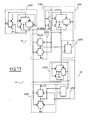
- FIG. 7 schematically represents a complete adder-subtractor with four inputs (A i ), (B i ), (R i-1 S) and (R i-1 D) on a bit comprising 23 transistors , in accordance with the invention.
- the adder-subtractor 20 consists of an adder 22 and a subtractor 24.
- the adder 22 is identical to that described with reference to FIG. 3. It comprises a module 1600 calculating the exclusive OR signal (A i ⁇ B i ).
- the module 1600 consists of transistors arranged in the same way as those of the first means described with reference to FIG. 3.
- the adder 22 also includes a module 1800 calculating the sum (S i ) of the three input bits (A i ), (B i ) and (R i-1 S)).
- the module 1800 is made up of transistors arranged in the same way as those of the second means described with reference to FIG. 2.
- the adder 22 also includes a module 1900 calculating the downstream transfer (R i S) associated with the sum of the two bits input (A i , B i ).
- the module 1900 consists of transistors arranged in the same way as those of the third means 300 described with reference to FIG. 2.
- the adder 22 finally comprises a module 1700 inverting the exclusive OR signal supplemented by the two input bits ( A i ⁇ B i ).
- the module 1700 consists of transistors arranged in the same way as those of the pair 400 described with reference to FIG. 3.
- the subtractor 24 includes a module 2000 calculating the difference (D i ) of the two input bits (A i , B i ) taking into account the upstream carry (R i-1 D) and a module 2100 calculating the downstream carry ( R i D) associated with the difference of the two input bits (A i , B i ).
- the transistors of module 2000 are arranged in the same way as those of module 1400 described with reference to FIG. 6.
- the transistors of module 2100 are arranged in the same way as those of module 1500 described with reference to FIG. 6.
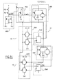
- FIG. 8 represents a complete adder-subtractor with four inputs (A i ), (B i ), (R i-1 S) and (R i-1 D) on a bit comprising 32 transistors according to the invention.
- the adder-subtractor 28 consists of an adder 30 and a subtractor 32.
- the adder 30 consists of a module 2200 calculating the exclusive OR signal of the two input bits (A i ⁇ B i ).
- the module 2200 is identical to that of the first means 100 described with reference to FIG. 2.
- the adder 30 also consists of a module 2300 calculating the sum of the two bits (S i ).
- the module 2300 is identical to the module calculating the sum (S i ) of the two bits described with reference to FIG. 4.
- the adder 30 also includes a module 2400 calculating the downstream carryover (R i S) associated with the sum of the three bits input (A i ), (B i ), (R i-1 S).
- the module 2400 is identical to the module 370 calculating the downstream transfer (R i S) associated with the sum of the two input bits described with reference to FIG. 5.
- the adder 30 finally comprises a module 2500 reversing the signal of exclusive OR of the two input bits (A i ⁇ B i ).
- the module 2500 is identical to the module 400 reversing the exclusive OR signal (A i ⁇ B i ) described with reference to FIG. 2.
- the subtractor 32 includes a module 2600 calculating the difference (D i ) of the two input bits and the upstream carry (R i-1 D).
- the module 2600 is identical to the module 2000 calculating the difference (D i ) of the two bits and of the upstream carry (R i-1 D) described with reference to FIG. 7.
- the subtractor 32 also includes a module 2800 calculating the downstream carryover (R i D) associated with the difference of the two bits (D i ).
- the module 2800 is identical to the module 2100 calculating the downstream carryover (R i D) associated with the difference of the two input bits.
- a module 2700 consisting of a P-channel transistor 2701 and an N-channel transistor 2702 is added to the upstream transfer input (R i-1 D) associated with the difference of the two input bits. also has downstream transfer signal (R i D) associated with the difference of the two bits, a module 2900 consisting of a transistor 2901 with P channel and a transistor 2902 with N channel.
- the transistors 2701 and 2702 of module 2700 and the transistors 2901 and 2902 of module 2900 are arranged so as to reverse the upstream carry signal (R i-1 D) and the downstream carry signal (R i D), respectively.
- Figure 9 represents a full adder-subtractor on a propagated bit with 31 transistors according to the invention.
- the adder-subtractor 34 comprises an adder 36 and a subtractor 38.
- the means 2250, 2260, 2270, 2280, 2290 and 2295 are identical respectively to the means 130, 460, 500, 260, 360 and 600 of the adder 6 described with reference to FIG. 4.
- the means 2350, 2360, 2370 and 2380 are identical respectively to the means 2600, 2700, 2800 and 2900 of the subtractor 32 described with reference to FIG. 8.
- the adder 36 calculates the signals of exclusive OR of the two input bits (A i ⁇ B i ) and its complement ( A i ⁇ B i ). These two signals are used by the subtractor 38 for the calculation of the difference of the two bits and the calculation of the carry (R i D) associated with the difference of the two bits.
- FIG. 10 represents a complete two-bit adder-subtractor comprising 55 transistors according to the invention.
- the two-bit adder-subtractor 40 is broken down into a one-bit adder-subtractor 42 and a one-bit adder-subtractor 48.
- the adder-subtractor 42 is identical to the adder-subtractor described with reference to FIG. 8.
- the adder-subtractor consists of a module 3000 calculating the exclusive OR signal of the two input bits (A i ⁇ B i ), of a module 3100 calculating the sum of the two input bits, and the upstream carry (R i-1 S) of a module 3200 calculating the downstream carryover (R i S) associated with the sum of the two bits , and of a module 3300 inverting the exclusive OR signal (A i ⁇ B i ).
- the adder-subtractor 42 also includes a module 3400 calculating the difference of the two bits (D i ) and a module 3500 calculating the downstream carryover (R i D) associated with the difference of the two bits.
- the adder-subtractor 48 is identical to the adder- subtractor described with reference to FIG. 9.
- the adder-subtractor 48 comprises a module 3600 calculating the exclusive OR signal ( A i + 1 ⁇ B i + 1 ), a module 3700 calculating the sum (S i + 1 ) of the two input bits (A i + 1 ) and (B i + 1 ) and the upstream carry (R i S), a module 3800 calculating the downstream carryover (R i + 1 S) associated with the sum of the two input bits (A i + 1 ) and (B i + 1 ) and a module 3900 inverting the exclusive OR signal complemented by the two bits ( A i + 1 ⁇ B i + 1 ).
- the adder-subtractor 48 also includes a module 4000 calculating the difference (D i + 1 ) of the two input bits and the upstream carry (R i D) and a module 4100 calculating the downstream carryover (R i + 1 D ) associated with the difference of the two input bits (A i + 1 ) and (B i + 1 ).
- the present invention also relates to a binary calculation device where the figures to be calculated are presented sequentially in series, that is to say one after the other, to the device. Each bit is shifted sequentially in the device under clock pulse control, starting with the least significant bit.
- a D type flip-flop is used, the operation of which is also controlled by the clock.
- FIG. 11 represents a schematic view of a complete adder with three sequential inputs on one bit comprising 16 transistors.
- the adder 50 firstly includes a module 5000 calculating the exclusive OR signal ( A i ⁇ B i ). It also includes a module 5100 calculating the sum of the two input bits and the downstream carry (R i-1 S). It then comprises a module 5200 calculating the downstream carryover (R i S) associated with the calculation of the sum of the three input bits (A i ), (B i ), (R i-1 S). Finally, it includes a module 5300 inverting the exclusive OR signal (A i ⁇ B i ). A D 5400 scale is interposed between the 5200 module and the 5100 module.
- flip-flop 5401 The input of flip-flop 5401 is connected to the downstream transfer (R i S).
- the output 5402 of the flip-flop D is connected to the upstream transfer (R i-1 S).
- the clock is connected to input 5403 of flip-flop D and the command to initialize flip-flop D is connected to input 5404.
- the flip-flop D described above works as follows:
- the application of the first clock pulse has the effect of presenting the least significant digit of the binary numbers at the inputs (A i ) and (B i ) of the adder.
- the sum (S i ) appears at the output of the adder and the downstream carry-over (R i S) is applied to the input 5401 of the flip-flop D.
- the next bit of the binary numbers is presented to the inputs (A i ) and (B i ) of the adder, the previous sum (S i ) is sent to a shift register (not shown), the previous downstream carry-over (R i S) is recorded by the flip-flop and is present at the upstream transfer input of the adder 50.
- the adder 52 includes a module 5500 calculating the exclusive OR signal complemented by the two input bits ( A i ⁇ B i ). It also includes a module 5600 calculating the sum of the three input bits (A i ), (B i ) and (R i-1 S). It then comprises a module 5700 calculating the downstream transfer (R i S) associated with the sum of the two input bits. It also includes a module 5800 inverting the exclusive OR signal, supplemented by the two input bits.
- D type flip-flop 5900 whose input 5901 is connected to the downstream transfer (R i S) and whose output 5902 is connected to the upstream transfer (R i-1 S).
- the clock is connected to input 5903 of flip-flop D and the command to initialize flip-flop D is connected to input 5904.
- FIG. 13 represents an adder-subtractor with four sequential inputs comprising 24 transistors according to the invention.
- the adder-subtractor 54 includes an adder 56 and a subtractor 58.
- the adder 56 is identical to the adder 50 described with reference to FIG. 11.
- the adder 56 includes a module 6000 calculating the exclusive OR signal of the two input bits.
- the adder 56 also includes a module 6100 calculating the sum of the three input bits (A i ), (B i ) and (R i-1 S). It also includes a module 6200 calculating the downstream transfer (R i S) associated with the sum of the two input bits. It also includes a module 6300 inverting the exclusive OR signal of the two input bits (A i ⁇ B i ).
- the subtractor 58 comprises a module 6500 calculating the difference (D i ) of the three input bits A i ), B i ) and (R i-1 D). It also includes a module 6600 calculating the downstream carryover (R i D) associated with the difference of the two input bits and it finally comprises a flip-flop 6700 whose input 6701 is connected to the downstream carryover (R i D) associated with the difference of the two input bits and whose output 6702 is connected to the upstream carry (R i-1 D) associated with the difference of the two input bits.
- FIG. 14 represents an adder-subtractor with four sequential inputs comprising 23 transistors according to the invention.
- the adder-subtractor 60 consists of an adder 62 and a subtractor 64.
- the adder 62 is identical to the adder described with reference to FIG. 12.
- the adder 62 comprises a module 6800 calculating the signal of Exclusive OR supplemented by the three input bits, a module 6900 calculating the sum of the two input bits (A i ), (B i ) and (R i-1 S), a module 7000 calculating the downstream carryover (R i S) associated with the sum of the two input bits, a module 7100 inverting the complemented exclusive OR signal of the two input bits ( A i ⁇ B i ) and a flip-flop 7200 storing the downstream transfer (R i S) associated with the sum of the two input bits.
- the subtractor 64 comprises a module 7300 calculating the difference (D i ) of the three input bits (A i ), (B i ) and (R i-1 D), a module 7400 calculating the downstream carryover (R i D) associated with the difference of the two input bits and a flip-flop 7500 of type D whose input 7501 is connected to the downstream carryover (R i D) associated with the difference of the two input bits and whose output is connected to the carryover upstream (R i-1 D) associated with the difference of the two input bits.
- the common characteristic of the device and its variants which is the subject of the invention which consists in producing the exclusive OR signal of the two bits (A i ⁇ B i ) once and reversing it by means of a pair of complementary transistors to achieve its complement ( A i ⁇ B i ), can therefore be advantageously applied to the production of the device with several cells arranged in add-on and / or subtractor modules with early carry-over.
- Another common characteristic of the device and of a major part of its variants is to use in common the additional outputs provided in the first and second means for supplying signals necessary for the downstream carry-over calculation (R i ) by the third means. , thereby reducing the number of transistors.
Landscapes
- Physics & Mathematics (AREA)
- General Physics & Mathematics (AREA)
- Engineering & Computer Science (AREA)
- Computational Mathematics (AREA)
- Mathematical Analysis (AREA)
- Pure & Applied Mathematics (AREA)
- Theoretical Computer Science (AREA)
- Computing Systems (AREA)
- Mathematical Optimization (AREA)
- General Engineering & Computer Science (AREA)
- Logic Circuits (AREA)
Applications Claiming Priority (2)
| Application Number | Priority Date | Filing Date | Title |
|---|---|---|---|
| FR8703758 | 1987-03-18 | ||
| FR8703758A FR2612660B1 (fr) | 1987-03-18 | 1987-03-18 | Dispositif de calcul binaire |
Publications (1)
| Publication Number | Publication Date |
|---|---|
| EP0283393A1 true EP0283393A1 (de) | 1988-09-21 |
Family
ID=9349158
Family Applications (1)
| Application Number | Title | Priority Date | Filing Date |
|---|---|---|---|
| EP88400589A Ceased EP0283393A1 (de) | 1987-03-18 | 1988-03-11 | Binäre Rechnungseinrichtung |
Country Status (4)
| Country | Link |
|---|---|
| US (1) | US4920509A (de) |
| EP (1) | EP0283393A1 (de) |
| JP (1) | JPH01243117A (de) |
| FR (1) | FR2612660B1 (de) |
Families Citing this family (10)
| Publication number | Priority date | Publication date | Assignee | Title |
|---|---|---|---|---|
| US5301341A (en) * | 1990-11-28 | 1994-04-05 | International Business Machines Corporation | Overflow determination for three-operand alus in a scalable compound instruction set machine which compounds two arithmetic instructions |
| US5267187A (en) * | 1990-05-10 | 1993-11-30 | Xilinx Inc | Logic structure and circuit for fast carry |
| US5295090A (en) * | 1992-05-10 | 1994-03-15 | Xilinx, Inc. | Logic structure and circuit for fast carry |
| US5818747A (en) * | 1995-01-27 | 1998-10-06 | Sun Microsystems, Inc. | Small, fast CMOS 4-2 carry-save adder cell |
| US5789781A (en) * | 1995-02-27 | 1998-08-04 | Alliedsignal Inc. | Silicon-on-insulator (SOI) semiconductor device and method of making the same |
| US7185042B1 (en) * | 2001-11-09 | 2007-02-27 | National Semiconductor Corporation | High speed, universal polarity full adder which consumes minimal power and minimal area |
| NL1020289C2 (nl) * | 2002-04-02 | 2003-10-03 | Jan Hendrik Van De Pol | Inrichting voor het optellen of aftrekken. |
| WO2006085039A1 (fr) * | 2005-02-14 | 2006-08-17 | France Telecom | Procede et dispositif de gestion de flot dans un reseau de telecommunications par paquets |
| RU2553221C2 (ru) * | 2013-06-13 | 2015-06-10 | Борис Михайлович Власов | Способы выполнения элементарных вычислительных операций (эво) и устройство их осуществления |
| RU2641218C1 (ru) * | 2016-12-02 | 2018-01-16 | Татьяна Алексеевна Малышева | Способы выполнения вычислительных операций (во) и устройство их реализации |
Citations (4)
| Publication number | Priority date | Publication date | Assignee | Title |
|---|---|---|---|---|
| US3767906A (en) * | 1972-01-21 | 1973-10-23 | Rca Corp | Multifunction full adder |
| EP0096333A2 (de) * | 1982-06-03 | 1983-12-21 | Kabushiki Kaisha Toshiba | Volladdierer |
| EP0143456A2 (de) * | 1983-11-28 | 1985-06-05 | Kabushiki Kaisha Toshiba | Paralleladdierschaltung |
| EP0185504A2 (de) * | 1984-12-14 | 1986-06-25 | RCA Thomson Licensing Corporation | Binäre Subtrahierschaltung |
Family Cites Families (10)
| Publication number | Priority date | Publication date | Assignee | Title |
|---|---|---|---|---|
| US3932734A (en) * | 1974-03-08 | 1976-01-13 | Hawker Siddeley Dynamics Limited | Binary parallel adder employing high speed gating circuitry |
| JPS5841533B2 (ja) * | 1975-10-31 | 1983-09-13 | 日本電気株式会社 | ゼンカゲンサンカイロ |
| US4052604A (en) * | 1976-01-19 | 1977-10-04 | Hewlett-Packard Company | Binary adder |
| FR2485832A1 (fr) * | 1980-06-24 | 1981-12-31 | Thomson Csf | Inverseur logique, et operateur a plusieurs sorties derive de cet inverseur, utilisant au moins un transistor a effet de champ a faible tension de seuil |
| US4369500A (en) * | 1980-10-20 | 1983-01-18 | Motorola Inc. | High speed NXM bit digital, repeated addition type multiplying circuit |
| US4471454A (en) * | 1981-10-27 | 1984-09-11 | Ibm Corporation | Fast, efficient, small adder |
| JPS6021629A (ja) * | 1983-07-15 | 1985-02-04 | Mitsubishi Electric Corp | 論理回路 |
| US4709346A (en) * | 1985-04-01 | 1987-11-24 | Raytheon Company | CMOS subtractor |
| US4713790A (en) * | 1985-07-31 | 1987-12-15 | Motorola, Inc. | Exclusive OR/NOR gate having cross-coupled transistors |
| US4739503A (en) * | 1986-04-21 | 1988-04-19 | Rca Corporation | Carry/borrow propagate adder/subtractor |
-
1987
- 1987-03-18 FR FR8703758A patent/FR2612660B1/fr not_active Expired - Lifetime
-
1988
- 1988-03-11 US US07/167,787 patent/US4920509A/en not_active Expired - Fee Related
- 1988-03-11 EP EP88400589A patent/EP0283393A1/de not_active Ceased
- 1988-03-18 JP JP63063742A patent/JPH01243117A/ja active Pending
Patent Citations (4)
| Publication number | Priority date | Publication date | Assignee | Title |
|---|---|---|---|---|
| US3767906A (en) * | 1972-01-21 | 1973-10-23 | Rca Corp | Multifunction full adder |
| EP0096333A2 (de) * | 1982-06-03 | 1983-12-21 | Kabushiki Kaisha Toshiba | Volladdierer |
| EP0143456A2 (de) * | 1983-11-28 | 1985-06-05 | Kabushiki Kaisha Toshiba | Paralleladdierschaltung |
| EP0185504A2 (de) * | 1984-12-14 | 1986-06-25 | RCA Thomson Licensing Corporation | Binäre Subtrahierschaltung |
Non-Patent Citations (3)
| Title |
|---|
| INTERNATIONAL JOURNAL OF MINI & MICROCOMPUTERS, vol. 7, no. 2, 1985, pages 49-52, Anaheim, California, US; D.I. MOLDOVAN et al.: "Bit serial techniques in VLSI parallel processing" * |
| PATENT ABSTRACTS OF JAPAN, vol. 9, no. 140 (E-321)[1863], 14 juin 1985; & JP-A-60 021 629 (MITSUBISHI DENKI K.K.) 04-02-1985 * |
| PROCEEDINGS OF THE IEEE INTERNATIONAL CONFERENCE ON COMPUTER DESIGN: VLSI IN COMPUTERS, ICCD' 85, New York, 7-10 octobre 1985, pages 359-362, IEEE; S. STEINLECHNER et al.: "Carry-save adders and their application for a multiplication with factored multiplicands" * |
Also Published As
| Publication number | Publication date |
|---|---|
| FR2612660B1 (fr) | 1990-10-19 |
| US4920509A (en) | 1990-04-24 |
| JPH01243117A (ja) | 1989-09-27 |
| FR2612660A1 (fr) | 1988-09-23 |
Similar Documents
| Publication | Publication Date | Title |
|---|---|---|
| FR2534045A1 (fr) | Circuit additionneur numerique | |
| FR2593652A1 (fr) | Reseau logique programmable a logique dynamique a horloge unique. | |
| EP0660525A1 (de) | Baumstruktur mit logischen Gattern des Typs "Exclusiv-ODER" und diese enthaltender Frequenzmultiplizierer | |
| EP0298002B1 (de) | Transpositionsspeicher für eine Datenverarbeitungsschaltung | |
| EP0847626B1 (de) | Vorrichtung zur digitalverarbeitung eines analogsignals, welches auch wieder in analoger form ausgegeben werden soll | |
| FR2612660A1 (fr) | Dispositif de calcul binaire | |
| FR2604270A1 (fr) | Additionneur binaire comportant un operande fixe, et multiplieur binaire parallele-serie comprenant un tel additionneur | |
| EP0051525B1 (de) | Logische Anordnung mit vereinfachter elektrischer Programmierung | |
| EP0042777A1 (de) | Logischer Inverter und Operator mit mehreren Ausgängen, wobei wenigstens ein Feldeffekttransistor mit niedriger Schwelle verwendet wird | |
| FR2624282A1 (fr) | Comparateur binaire et operateur de tri de nombres binaires | |
| EP0905907B1 (de) | Exklusiv-Oder-Gatter mit vier zwei-zu-zwei komplementären Eingängen und zwei komplementären Ausgängen sowie Frequenzmultiplizierer damit | |
| EP0309348B1 (de) | Binäre Additions- und Multiplikationsvorrichtung | |
| BE898544R (fr) | Calculateur associatif permettant une multiplication rapide. | |
| FR2550671A1 (fr) | Circuit convertisseur analogique-numerique et demodulateur de signaux video modules en argument | |
| EP0447729B1 (de) | Gegen Rauschen geschützter Schwellwertdetektor | |
| EP0068059A1 (de) | Exklusiv-Oder-Schaltung und ihre Anwendung in einer Paritätenauswertungsschaltung | |
| FR2599526A1 (fr) | Additionneur mos et multiplicateur binaire mos comprenant au moins un tel additionneur | |
| FR2624283A1 (fr) | Circuit integre de calcul numerique pour calculs glissants du type convolution | |
| EP0327445A1 (de) | Allgemeiner digitaler Multiplizierer und digitaler Filter mit diesem Multiplizierer | |
| FR2656964A1 (fr) | Doubleur/diviseur d'un flux de bits serie. | |
| FR2604577A1 (fr) | Circuit generateur de code a bruit pseudo-aleatoire | |
| FR2563349A1 (fr) | Multiplieur matriciel systolique de traitement de donnees numeriques | |
| EP0175623A1 (de) | Einrichtung zur Echtzeitdigitalsignalverarbeitung durch Faltung | |
| EP0237414B1 (de) | Elementarer Binärzähler, synchroner Binärzähler und Frequenzteiler unter Verwendung des elementaren Binärzählers | |
| EP0065460B1 (de) | Parallelzähler in integrierter MOS-Schaltung und seine Anwendung in einem Binäraddierer |
Legal Events
| Date | Code | Title | Description |
|---|---|---|---|
| PUAI | Public reference made under article 153(3) epc to a published international application that has entered the european phase |
Free format text: ORIGINAL CODE: 0009012 |
|
| AK | Designated contracting states |
Kind code of ref document: A1 Designated state(s): DE FR GB NL |
|
| 17P | Request for examination filed |
Effective date: 19890105 |
|
| 17Q | First examination report despatched |
Effective date: 19900927 |
|
| STAA | Information on the status of an ep patent application or granted ep patent |
Free format text: STATUS: THE APPLICATION HAS BEEN REFUSED |
|
| 18R | Application refused |
Effective date: 19910627 |