EP0706165B1 - Filtre pour la diffusion d'erreur de DMD pour l'utilisation dans un systéme d'affichage - Google Patents
Filtre pour la diffusion d'erreur de DMD pour l'utilisation dans un systéme d'affichage Download PDFInfo
- Publication number
- EP0706165B1 EP0706165B1 EP95115269A EP95115269A EP0706165B1 EP 0706165 B1 EP0706165 B1 EP 0706165B1 EP 95115269 A EP95115269 A EP 95115269A EP 95115269 A EP95115269 A EP 95115269A EP 0706165 B1 EP0706165 B1 EP 0706165B1
- Authority
- EP
- European Patent Office
- Prior art keywords
- error
- pixel
- intensity level
- output value
- pixel elements
- Prior art date
- Legal status (The legal status is an assumption and is not a legal conclusion. Google has not performed a legal analysis and makes no representation as to the accuracy of the status listed.)
- Expired - Lifetime
Links
- 238000009792 diffusion process Methods 0.000 title claims description 19
- 230000002950 deficient Effects 0.000 claims description 15
- 238000000034 method Methods 0.000 claims description 8
- 230000007547 defect Effects 0.000 claims description 4
- 238000001914 filtration Methods 0.000 claims description 2
- 230000004044 response Effects 0.000 description 7
- 238000010586 diagram Methods 0.000 description 3
- 230000005540 biological transmission Effects 0.000 description 2
- 230000000694 effects Effects 0.000 description 2
- 230000003068 static effect Effects 0.000 description 2
- 230000004075 alteration Effects 0.000 description 1
- 230000015556 catabolic process Effects 0.000 description 1
- 239000003086 colorant Substances 0.000 description 1
- 238000006731 degradation reaction Methods 0.000 description 1
- 230000001934 delay Effects 0.000 description 1
- 230000006870 function Effects 0.000 description 1
- 238000003384 imaging method Methods 0.000 description 1
- 230000000116 mitigating effect Effects 0.000 description 1
- 230000007935 neutral effect Effects 0.000 description 1
- 238000012805 post-processing Methods 0.000 description 1
- 238000012545 processing Methods 0.000 description 1
- 239000004065 semiconductor Substances 0.000 description 1
- 238000001228 spectrum Methods 0.000 description 1
- 238000006467 substitution reaction Methods 0.000 description 1
- 230000002123 temporal effect Effects 0.000 description 1
- 230000000007 visual effect Effects 0.000 description 1
Images


Classifications
-
- H—ELECTRICITY
- H04—ELECTRIC COMMUNICATION TECHNIQUE
- H04N—PICTORIAL COMMUNICATION, e.g. TELEVISION
- H04N3/00—Scanning details of television systems; Combination thereof with generation of supply voltages
- H04N3/02—Scanning details of television systems; Combination thereof with generation of supply voltages by optical-mechanical means only
-
- G—PHYSICS
- G09—EDUCATION; CRYPTOGRAPHY; DISPLAY; ADVERTISING; SEALS
- G09G—ARRANGEMENTS OR CIRCUITS FOR CONTROL OF INDICATING DEVICES USING STATIC MEANS TO PRESENT VARIABLE INFORMATION
- G09G3/00—Control arrangements or circuits, of interest only in connection with visual indicators other than cathode-ray tubes
- G09G3/20—Control arrangements or circuits, of interest only in connection with visual indicators other than cathode-ray tubes for presentation of an assembly of a number of characters, e.g. a page, by composing the assembly by combination of individual elements arranged in a matrix no fixed position being assigned to or needed to be assigned to the individual characters or partial characters
- G09G3/34—Control arrangements or circuits, of interest only in connection with visual indicators other than cathode-ray tubes for presentation of an assembly of a number of characters, e.g. a page, by composing the assembly by combination of individual elements arranged in a matrix no fixed position being assigned to or needed to be assigned to the individual characters or partial characters by control of light from an independent source
- G09G3/3433—Control arrangements or circuits, of interest only in connection with visual indicators other than cathode-ray tubes for presentation of an assembly of a number of characters, e.g. a page, by composing the assembly by combination of individual elements arranged in a matrix no fixed position being assigned to or needed to be assigned to the individual characters or partial characters by control of light from an independent source using light modulating elements actuated by an electric field and being other than liquid crystal devices and electrochromic devices
- G09G3/346—Control arrangements or circuits, of interest only in connection with visual indicators other than cathode-ray tubes for presentation of an assembly of a number of characters, e.g. a page, by composing the assembly by combination of individual elements arranged in a matrix no fixed position being assigned to or needed to be assigned to the individual characters or partial characters by control of light from an independent source using light modulating elements actuated by an electric field and being other than liquid crystal devices and electrochromic devices based on modulation of the reflection angle, e.g. micromirrors
-
- G—PHYSICS
- G02—OPTICS
- G02B—OPTICAL ELEMENTS, SYSTEMS OR APPARATUS
- G02B26/00—Optical devices or arrangements for the control of light using movable or deformable optical elements
- G02B26/08—Optical devices or arrangements for the control of light using movable or deformable optical elements for controlling the direction of light
- G02B26/0816—Optical devices or arrangements for the control of light using movable or deformable optical elements for controlling the direction of light by means of one or more reflecting elements
- G02B26/0833—Optical devices or arrangements for the control of light using movable or deformable optical elements for controlling the direction of light by means of one or more reflecting elements the reflecting element being a micromechanical device, e.g. a MEMS mirror, DMD
- G02B26/0841—Optical devices or arrangements for the control of light using movable or deformable optical elements for controlling the direction of light by means of one or more reflecting elements the reflecting element being a micromechanical device, e.g. a MEMS mirror, DMD the reflecting element being moved or deformed by electrostatic means
-
- G—PHYSICS
- G09—EDUCATION; CRYPTOGRAPHY; DISPLAY; ADVERTISING; SEALS
- G09G—ARRANGEMENTS OR CIRCUITS FOR CONTROL OF INDICATING DEVICES USING STATIC MEANS TO PRESENT VARIABLE INFORMATION
- G09G3/00—Control arrangements or circuits, of interest only in connection with visual indicators other than cathode-ray tubes
- G09G3/20—Control arrangements or circuits, of interest only in connection with visual indicators other than cathode-ray tubes for presentation of an assembly of a number of characters, e.g. a page, by composing the assembly by combination of individual elements arranged in a matrix no fixed position being assigned to or needed to be assigned to the individual characters or partial characters
- G09G3/2007—Display of intermediate tones
- G09G3/2059—Display of intermediate tones using error diffusion
-
- H—ELECTRICITY
- H04—ELECTRIC COMMUNICATION TECHNIQUE
- H04N—PICTORIAL COMMUNICATION, e.g. TELEVISION
- H04N9/00—Details of colour television systems
- H04N9/12—Picture reproducers
- H04N9/31—Projection devices for colour picture display, e.g. using electronic spatial light modulators [ESLM]
- H04N9/3102—Projection devices for colour picture display, e.g. using electronic spatial light modulators [ESLM] using two-dimensional electronic spatial light modulators
- H04N9/3111—Projection devices for colour picture display, e.g. using electronic spatial light modulators [ESLM] using two-dimensional electronic spatial light modulators for displaying the colours sequentially, e.g. by using sequentially activated light sources
- H04N9/3114—Projection devices for colour picture display, e.g. using electronic spatial light modulators [ESLM] using two-dimensional electronic spatial light modulators for displaying the colours sequentially, e.g. by using sequentially activated light sources by using a sequential colour filter producing one colour at a time
-
- H—ELECTRICITY
- H04—ELECTRIC COMMUNICATION TECHNIQUE
- H04N—PICTORIAL COMMUNICATION, e.g. TELEVISION
- H04N9/00—Details of colour television systems
- H04N9/12—Picture reproducers
- H04N9/31—Projection devices for colour picture display, e.g. using electronic spatial light modulators [ESLM]
- H04N9/3179—Video signal processing therefor
- H04N9/3182—Colour adjustment, e.g. white balance, shading or gamut
-
- G—PHYSICS
- G09—EDUCATION; CRYPTOGRAPHY; DISPLAY; ADVERTISING; SEALS
- G09G—ARRANGEMENTS OR CIRCUITS FOR CONTROL OF INDICATING DEVICES USING STATIC MEANS TO PRESENT VARIABLE INFORMATION
- G09G2320/00—Control of display operating conditions
- G09G2320/02—Improving the quality of display appearance
- G09G2320/0271—Adjustment of the gradation levels within the range of the gradation scale, e.g. by redistribution or clipping
- G09G2320/0276—Adjustment of the gradation levels within the range of the gradation scale, e.g. by redistribution or clipping for the purpose of adaptation to the characteristics of a display device, i.e. gamma correction
Definitions
- This invention relates to digital imaging and more particularly to an error diffusion filter for a digital micromirror device (DMD) display of the type defined in the precharacterizing portion of claim 1.
- DMD digital micromirror device
- a new projection display that utilizes reflections from hundreds of thousands of micromirrors, each mounted above its own semiconductor memory cell is described in IEEE Spectrum, November 1993, vol. 30, no. 11, written by Jack M. Younse of Texas Instruments Incorporated.
- the digital micromirror device comprises a special light modulator that was invented in 1987 by Larry J. Hornbeck, a Texas Instruments Incorporated scientist.
- the DMD, or digital micromirror device covers each memory cell of a CMOS static RAM with a movable micromirror. Electrostatic forces based on the data in this cell tilt the mirror either plus or minus 10 degrees, modulating the light incident on the surface.
- the light reflected from any of the mirrors passes through a projection lens and creates an image on a large screen.
- Light from the remaining off mirrors is reflected away from the projection lens and trapped.
- the portion of the time during each video frame that the mirror remains in the on state determines the shades of grey- from black for zero on time to white for 100 percent on time. Color may be added in two ways, by a color wheel or a 3-DMD set up.
- Some DMD devices may have the capability to display only a low number of bits representing the on and off times and, therefore, the shades of grey or shades of color, leading to degradation of the video quality. Also, the use of digital degamma in the DMD display systems entails some loss of resolution (blockiness) in the low intensity regions. Finally, even the best of DMDs can have some defects (pixels stuck on, off, or flat). It is desirable to find some method to provide a correction for these display errors and to provide a more pleasing picture without significantly increasing the time for processing by increasing the number of bits for each on or off time.
- An error diffusion filter of the type defined in the precharacterizing portion of claim 1 is known from WO-A-9209064. Using that error diffusion filter, bits having a duration of less than the shortest displayable duration can be displayed by adjusting the turn-on time of a proportion of the adjacent mirrors.
- a method of mitigating the effects of a bright defective electromechanical pixel which transmits light into an observer's field of view comprises the step of applying a voltage sufficient to damage the electromechanical pixel, which has a beam and a hinge, in such a manner that the pixel no longer transmits light into the observer's field of view.
- the problem of low number of bits, blockiness due to degamma and DMD defects is alleviated by an improved diffusion filter.
- the improved filter includes both an inverse gamma look-up table and an error look-up table that is responsive to the video data for providing an error value that is distributed to neighboring pixel elements.
- FIG. 1 there is illustrated an overall block diagram of a digital micromirror device (DMD) display system.
- DMD digital micromirror device
- FIG. 1 an example of a DMD system 10 is illustrated, wherein the light from a light source 11 is applied through a first condenser lens 13 and through a color wheel 15, which is rotating at about sixty cycles, or hertz, or 60 frames per second.
- the light passing through the color wheel 15 passes through a second condenser lens 17 onto a DMD chip 19.
- the DMD chip includes an array of tiny mirror elements, or micromirrors, where each mirror element is hinged by a torsion hinge and support post above a memory cell of a CMOS static RAM as shown in Fig. 2.
- the movable micromirror tilts into the on or off states by electrostatic forces based on data in the cell.
- the tilt of the mirror is either plus 10 degrees (on) or minus 10 degrees (off) to modulate the light that is incident on the surface.
- the light reflected from any of the mirrors may pass through a projection lens 20 and create images on a large screen 21.
- the portion of time during which the video frame that a mirror remains in the on state determines the shade of grey.
- the time duration in which the cell is in the positive direction, or on, is represented by 8 bits of data sent to that cell.
- the color wheel 15 is divided into red, green, and blue sectors.
- the maximum red would be when the red, for example, would be reflecting the maximum period of time as when the light is on the longest period of time in the red sector.
- Applicants' invention can also be used in DMD display systems that use three DMD displays in place of a color wheel. The same would go for the other two colors. The minimum would be where the micromirror would not be reflecting through the color wheel and the lens, etc. at all during the color cycle.
- the intensity resolution in this pulse width modulation (PWM) is limited by the response time of the DMD mirrors.
- the total time available to display a color frame and the least time required to turn a mirror to the "on" state and back to "off” state defines the resolution of present systems.
- the most significant bit as illustrated in Fig. 3, is the 7th bit with that bit representing the widest "on” time, the 6th bit being then the next widest "on” time, and the 5th bit representing the third longest "on” time, etc., all the way down to the least significant 0 bit, which is represented by the shortest time period.
- a sequential color DMD system might have 5 (five) msec (milliseconds) available for a color frame.
- the least significant bit (0 bit on only), the shortest period would be "on" for about 19.6 microseconds.
- the mirror on/off time would have to be less than 19.6 msec to implement this scheme with the current method.
- the system would have too few number of grades of grey or shades of color and, therefore, tend to show blockiness between portions of the picture. This would represent one of the errors that the present invention is to overcome.
- This degamma correction is done, for example, for each color by providing the raster scanned gamma corrected red, green, or blue video data as shown in Fig. 1 to a separate degamma look-up table (LUT) 50 where for given input threshold levels the mirrors are turned on for given durations.
- LUT degamma look-up table
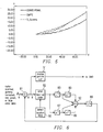
- the output is stepped as shown in Fig. 5 rather than smooth between the thresholds of the bits and, therefore, the grade levels again take on a blockiness particularly in the low intensity regions.
- Applicants solve the problems of the low number of bits and blockiness due to degamma, and defective DMDs by an error diffusion filter, as shown in Fig. 6 (FIL in Fig. 1), for each color path (red, green, and blue) on the raster scanned video output that would normally be written into the frame RAM buffer 53.
- an output intensity N will be displayed on the DMD device. If the degamma was perfect and there was no lack of bits, the value displayed on the DMD would be some other value N1.
- Temporal error diffusion can be a post processing step in this algorithm to improve frame to frame visual response and is being investigated.
- error diffusion filter according to one embodiment of the present invention.
- the difference between N and N1 is distributed among its neighboring pixels as illustrated in Fig. 7.
- the implementation is illustrated in Fig. 6 wherein the raster scan gamma corrected red, green, or blue video 8-bit pixel intensity level data is applied, for example, via summer device 81 to both an error look-up table 82 and inverse gamma look-up (LUT) 51.
- a perfect inverse gamma is known and follows Curve A.
- Table 2 in Appendix A for a 8-bit display shows for a given input value (IN) the value N provided by LUT 51 is in column marked “OUT” and is applied to corresponding DMD device.
- the error or difference value from the ideal N1 is N - N1 and is taken from the error look-up table (LUT) 82 and for an 8-bit display the value is marked as "ERROR” in Table 2.
- the input data value is 38
- the output value from LUT 51 is 8 and the error value from Error LUT Table 82 is 1. This error is distributed for example as indicated in Fig. 7.
- the value of pixel 90 has one-quarter of the error from the previous horizontal line r-1 and previous column c-1 via H-1 delay 83 and V-1 delay 85, respectively, divider 88 and summer 92.
- the value at Pixel 90 has one-quarter of the error from the previous picture element in the column C-1 and this value is applied to summer 81 via H-1 delay 83, divider 88 and summer 92.
- Another one-quarter of the error from the previous line and same column is provided over V-1 delay 87 and divider 88.
- Another quarter of the error from the previous horizontal line R-1 and the next or C+1 column is applied via V-1 delay 87, H+1 delay 89 and divider 88.
- the H-1 delay is for one pixel delay
- the V-1 delay is one line delay
- the H+1 delay would reduce the V-1 delay by one pixel delay. This could be done by a separate FIFO delay by parsing V-1 delay 87. In this manner, the error added at summer 81 enhances the apparent intensity resolution of the video display system at the adjacent pixels.
- the Tables 51 and 82 provide the values of Table 3 of Appendix A.
- a further advantage of the present invention is that the defect compensation can be performed as part of this algorithm.
- a defective pixel is corrected for by treating this as an error.
- the DMD coordinates of defective pixels at source 95 is provided to look-up table 82 and the error diffusion needs to be modified to account for the fact that at those locations the pixel displays either bright (stuck ON), dark (stuck OFF), or neutral (flat pixel).
- the surrounding pixels to the defective pixels are modified in intensity to correct for the failed position of the micromirrors.
- the look-up table LUT 82 stores error values for these defective locations based on the type of error and the neighboring pixels are modified at summer 81.
- the error is distributed as discussed previously, such as the distribution as in Fig. 7 by the delays and summer 92 and divider of Fig. 6.
Landscapes
- Engineering & Computer Science (AREA)
- Physics & Mathematics (AREA)
- General Physics & Mathematics (AREA)
- Multimedia (AREA)
- Signal Processing (AREA)
- Computer Hardware Design (AREA)
- Theoretical Computer Science (AREA)
- Optics & Photonics (AREA)
- Control Of Indicators Other Than Cathode Ray Tubes (AREA)
- Mechanical Light Control Or Optical Switches (AREA)
- Projection Apparatus (AREA)
- Transforming Electric Information Into Light Information (AREA)
Claims (8)
- Filtre de diffusion d'erreur pour un dispositif d'affichage DMD comprenant :caractérisé en ce que ladite table de consultation de gamma inverse (51) est apte à répondre à des données vidéo explorées selon un balayage de trame et ayant subi une correction de gamma, pour délivrer un niveau numérisé d'intensité de données de pixels audit élément de pixel donné, ledit niveau numérisé d'intensité étant le niveau d'intensité de données de pixels le plus proche pouvant être obtenu par rapport à un niveau d'intensité précis de gamma inverse; etune table de consultation de gamma inverse (51) ; etdes moyens aptes à répondre à une valeur de sortie d'erreur pour modifier de façon distributive des niveaux d'intensité de données de pixels à des éléments de pixels voisins d'un élément de pixel donné d'un dispositif DMD (19), ladite modification étant proportionnelle à ladite valeur de sortie d'erreur;
que ledit filtre de diffusion d'erreur comporte en outre une table de consultation d'erreurs (82) apte à répondre auxdites données vidéo pour délivrer ladite valeur de sortie d'erreur, ladite valeur de sortie d'erreur correspondant à la différence entre ledit niveau d'intensité de gamma inverse précis et ledit niveau d'intensité le plus proche pouvant être obtenu immédiatement pour ledit élément de pixel donné. - Filtre de diffusion d'erreur selon la revendication 1, dans lequel ladite table de consultation d'erreur (82) comprend en outre une table fournissant des valeurs d'erreurs basées sur l'emplacement d'éléments de pixels défectueux et dans lequel lesdits moyens de modification de niveaux d'intensité de données de pixels incluent des moyens aptes à répondre auxdites valeurs d'erreurs sur la l'emplacement desdits éléments de pixels défectueux pour modifier le niveau d'intensité de données de pixels sur des éléments de pixels entourant chacun desdits éléments de pixels défectueux pour réaliser un ajustement visuel desdits éléments de pixels défectueux.
- Filtre de diffusion d'erreurs selon la revendication 1 ou la revendication 2, dans lequel lesdits moyens sensibles à la valeur de sortie d'erreur incluent, pour modifier un élément de pixel voisin, des moyens (92) pour faire la sommation de 1/4 de l'erreur provenant d'un élément de données de pixel horizontal donné précédent, de 1/4 de l'erreur provenant d'un élément de données de pixel vertical donné; de 1/4 de l'erreur entre l'élément de données de pixel horizontal précédent et ledit élément de données de pixel vertical précédent, et de 1/4 de l'erreur entre l'élément de données horizontal donné suivant et ledit élément de données de pixels vertical précédent.
- Filtre de diffusion d'erreur selon la revendication 3, dans lequel lesdits moyens (92) de sommation incluent un retard de ligne (85,87).
- Filtre de diffusion d'erreur selon l'une quelconque des revendications précédentes, dans lequel il est prévu une table de consultation de gamma inverse séparée et une opération de diffusion pour les données vidéo rouge, verte et bleue.
- Filtre de diffusion d'erreur selon l'une quelconque des revendications précédentes, dans lequel les moyens sensibles à une sortie d'erreur comprennent :
un dispositif de sommation (81) couplé à des éléments de pixels voisins dudit élément de pixel donné et apte à répondre à ladite valeur de sortie d'erreur pour réaliser la sommation de ladite valeur de sortie d'erreur et des niveaux d'intensité de données de pixels pour lesdits éléments de pixels voisins pour obtenir visuellement ledit niveau d'intensité de gamma inverse précis. - Procédé pour filtrer un dispositif d'affichage DMD comprenant les étapes consistant à :appliquer un niveau d'intensité de pixel numérisé à chaque élément de pixel qui possède le niveau d'intensité le plus proche d'un niveau d'intensité de gamma inverse précis en utilisant une table de consultation de gamma inverse (51) ;produire une valeur de sortie d'erreur correspondant à la différence entre ledit niveau d'intensité précis et le niveau d'intensité le plus proche pouvant être obtenu, en utilisant une table de consultation d'erreurs (82) ; etmodifier les niveaux d'intensité de données de pixels pour les appliquer à des éléments de pixels entourant des éléments de pixels présentant une valeur de sortie d'erreur, lesdits éléments de pixels disposés alentour étant modifiés d'une manière proportionnelle à ladite valeur de sortie d'erreur.
- Procédé pour corriger des éléments de pixels défectueux dans un dispositif d'affichage DMD, comprenant les étapes consistant à :déterminer l'emplacement de chacun desdits éléments de pixels défectueux;mémoriser les valeurs d'erreurs dans une table (82) sur la base de l'emplacement de chacun desdits éléments de pixels défectueux; etmodifier les niveaux d'intensité de pixels d'éléments de pixels entourant chacun desdits éléments de pixels défectueux pour ajuster visuellement le défaut.
Applications Claiming Priority (2)
| Application Number | Priority Date | Filing Date | Title |
|---|---|---|---|
| US08/315,744 US5623281A (en) | 1994-09-30 | 1994-09-30 | Error diffusion filter for DMD display |
| US315744 | 1994-09-30 |
Publications (2)
| Publication Number | Publication Date |
|---|---|
| EP0706165A1 EP0706165A1 (fr) | 1996-04-10 |
| EP0706165B1 true EP0706165B1 (fr) | 2001-11-28 |
Family
ID=23225866
Family Applications (1)
| Application Number | Title | Priority Date | Filing Date |
|---|---|---|---|
| EP95115269A Expired - Lifetime EP0706165B1 (fr) | 1994-09-30 | 1995-09-27 | Filtre pour la diffusion d'erreur de DMD pour l'utilisation dans un systéme d'affichage |
Country Status (5)
| Country | Link |
|---|---|
| US (1) | US5623281A (fr) |
| EP (1) | EP0706165B1 (fr) |
| JP (1) | JPH08214243A (fr) |
| KR (1) | KR100350028B1 (fr) |
| DE (1) | DE69524184T2 (fr) |
Families Citing this family (35)
| Publication number | Priority date | Publication date | Assignee | Title |
|---|---|---|---|---|
| JP3139312B2 (ja) * | 1994-11-25 | 2001-02-26 | 株式会社富士通ゼネラル | ディスプレイ駆動方法および装置 |
| US7253794B2 (en) * | 1995-01-31 | 2007-08-07 | Acacia Patent Acquisition Corporation | Display apparatus and method |
| US6052491A (en) | 1996-01-26 | 2000-04-18 | Texas Instruments Incorporated | Non-monotonic contour diffusion and algorithm |
| JP3519853B2 (ja) * | 1996-02-28 | 2004-04-19 | 富士写真フイルム株式会社 | マイクロミラー式画像形成装置及びその管理方法 |
| US6057933A (en) * | 1997-10-30 | 2000-05-02 | Hewlett-Packard Company | Table based fast error diffusion halftoning technique |
| US6342898B1 (en) * | 1998-03-16 | 2002-01-29 | Texas Instruments Incorporated | Compression and decompression of degamma tables for projection systems |
| US6271957B1 (en) * | 1998-05-29 | 2001-08-07 | Affymetrix, Inc. | Methods involving direct write optical lithography |
| US6657758B1 (en) | 1998-06-04 | 2003-12-02 | Board Of Regents, The University Of Texas System | Variable spectrum generator system |
| EP0989537B1 (fr) * | 1998-09-22 | 2007-06-27 | Matsushita Electric Industrial Co., Ltd. | Méthode améliorée d'affichage d'images à gradations multiples |
| TW575855B (en) * | 1999-08-05 | 2004-02-11 | Sharp Kk | Display device |
| JP5127089B2 (ja) | 2000-10-17 | 2013-01-23 | キヤノン株式会社 | 表示装置、投射型表示装置、光変調装置の駆動装置、及び光変調装置の駆動方法 |
| US6700561B1 (en) * | 2000-10-31 | 2004-03-02 | Agilent Technologies, Inc. | Gamma correction for displays |
| US6970150B2 (en) * | 2001-03-19 | 2005-11-29 | Texas Instruments Incorporated | Control timing for spatial light modulator |
| US7076110B2 (en) * | 2001-08-09 | 2006-07-11 | Texas Instruments Incorporated | Quantization error diffusion for digital imaging devices |
| US7098927B2 (en) | 2002-02-01 | 2006-08-29 | Sharp Laboratories Of America, Inc | Methods and systems for adaptive dither structures |
| US8289233B1 (en) | 2003-02-04 | 2012-10-16 | Imaging Systems Technology | Error diffusion |
| US8305301B1 (en) | 2003-02-04 | 2012-11-06 | Imaging Systems Technology | Gamma correction |
| US7071908B2 (en) * | 2003-05-20 | 2006-07-04 | Kagutech, Ltd. | Digital backplane |
| US8243093B2 (en) | 2003-08-22 | 2012-08-14 | Sharp Laboratories Of America, Inc. | Systems and methods for dither structure creation and application for reducing the visibility of contouring artifacts in still and video images |
| US7164397B2 (en) * | 2003-09-30 | 2007-01-16 | Texas Instruments Incorporated | Discrete light color processor |
| US7352373B2 (en) * | 2003-09-30 | 2008-04-01 | Sharp Laboratories Of America, Inc. | Systems and methods for multi-dimensional dither structure creation and application |
| WO2005084033A1 (fr) * | 2004-02-04 | 2005-09-09 | Thomson Licensing S.A. | Diffusion d'erreur appliquee a la reduction de la dimension d'echantillon de video numerique |
| JP4289269B2 (ja) * | 2004-03-01 | 2009-07-01 | セイコーエプソン株式会社 | 光学表示装置、光学表示装置制御プログラム及び光学表示装置制御方法 |
| MY139438A (en) * | 2004-05-06 | 2009-09-30 | Thomson Licensing Sa | Pixel shift display with minimal noise |
| WO2005109387A2 (fr) * | 2004-05-06 | 2005-11-17 | Thomson Licensing | Affichage a decalage de pixels et a bruit minimal |
| US7474316B2 (en) * | 2004-08-17 | 2009-01-06 | Sharp Laboratories Of America, Inc. | Bit-depth extension of digital displays via the use of models of the impulse response of the visual system |
| JP4622425B2 (ja) * | 2004-09-29 | 2011-02-02 | セイコーエプソン株式会社 | 表示制御装置及び方法 |
| US20060066842A1 (en) * | 2004-09-30 | 2006-03-30 | Saunders Winston A | Wafer inspection with a customized reflective optical channel component |
| US9299284B2 (en) | 2004-11-10 | 2016-03-29 | Thomson Licensing | System and method for dark noise reduction in pulse width modulated (PWM) displays |
| US7336817B2 (en) * | 2005-06-20 | 2008-02-26 | Microsoft Corporation | Processing raw and pre-processed digital images |
| KR101255311B1 (ko) | 2006-06-29 | 2013-04-15 | 엘지디스플레이 주식회사 | 평판표시장치와 그 화질제어 방법 |
| US8004740B2 (en) | 2006-11-09 | 2011-08-23 | International Business Machines Corporation | Device and system for reflective digital light processing (DLP) |
| US8248328B1 (en) | 2007-05-10 | 2012-08-21 | Imaging Systems Technology | Plasma-shell PDP with artifact reduction |
| JP2009047965A (ja) * | 2007-08-21 | 2009-03-05 | Seiko Epson Corp | 画像処理装置、画像処理方法、表示装置およびプログラム |
| CN101304541B (zh) * | 2008-06-19 | 2010-06-02 | 浙江大学 | 基于柱镜光栅lcd自由立体显示设备的通用立体图像分解方法 |
Family Cites Families (7)
| Publication number | Priority date | Publication date | Assignee | Title |
|---|---|---|---|---|
| GB9005418D0 (en) * | 1990-03-10 | 1990-05-09 | Hydraulic Design Ltd | Method and apparatus for removing grit from sewage |
| GB9024978D0 (en) * | 1990-11-16 | 1991-01-02 | Rank Cintel Ltd | Digital mirror spatial light modulator |
| DE69213357T2 (de) * | 1991-06-27 | 1997-01-16 | Texas Instruments Inc | Modulationsverfahren für verformbare Spiegelvorrichtung (DMD) |
| DE69231194T2 (de) * | 1991-12-05 | 2001-02-15 | Texas Instruments Inc., Dallas | Verfahren zur Verbesserung eines Videosignals |
| US5289172A (en) * | 1992-10-23 | 1994-02-22 | Texas Instruments Incorporated | Method of mitigating the effects of a defective electromechanical pixel |
| KR960005016B1 (ko) * | 1992-11-26 | 1996-04-18 | 삼성전자주식회사 | 칼라 프린터에 있어서 적응칼라 에러 확산방법 및 회로 |
| US5452024A (en) * | 1993-11-01 | 1995-09-19 | Texas Instruments Incorporated | DMD display system |
-
1994
- 1994-09-30 US US08/315,744 patent/US5623281A/en not_active Expired - Lifetime
-
1995
- 1995-09-27 DE DE69524184T patent/DE69524184T2/de not_active Expired - Lifetime
- 1995-09-27 EP EP95115269A patent/EP0706165B1/fr not_active Expired - Lifetime
- 1995-09-29 KR KR1019950032769A patent/KR100350028B1/ko not_active Expired - Lifetime
- 1995-09-29 JP JP7253960A patent/JPH08214243A/ja active Pending
Also Published As
| Publication number | Publication date |
|---|---|
| DE69524184T2 (de) | 2002-07-04 |
| DE69524184D1 (de) | 2002-01-10 |
| US5623281A (en) | 1997-04-22 |
| KR960012929A (ko) | 1996-04-20 |
| KR100350028B1 (ko) | 2002-12-16 |
| EP0706165A1 (fr) | 1996-04-10 |
| JPH08214243A (ja) | 1996-08-20 |
Similar Documents
| Publication | Publication Date | Title |
|---|---|---|
| EP0706165B1 (fr) | Filtre pour la diffusion d'erreur de DMD pour l'utilisation dans un systéme d'affichage | |
| EP0704835B1 (fr) | Filtre de diffusion d'erreurs pour un affichage à miroirs déformables | |
| EP0823698B1 (fr) | Améliorations relatives à des systèmes d'affichage à miroir numériques | |
| US5657036A (en) | Color display system with spatial light modulator(s) having color-to color variations for split reset | |
| US5737038A (en) | Color display system with spatial light modulator(s) having color-to-color variations in the data bit weight sequence | |
| JP5174309B2 (ja) | 映写装置のダイナミックレンジを増大する装置および技術 | |
| US5497172A (en) | Pulse width modulation for spatial light modulator with split reset addressing | |
| US6008785A (en) | Generating load/reset sequences for spatial light modulator | |
| KR100346877B1 (ko) | 디지탈비디오시스템에서순간아티팩트를감소시키는방법및시스템 | |
| US5812303A (en) | Light amplitude modulation with neutral density filters | |
| US8717394B2 (en) | Boundary dispersion for mitigating PWM temporal contouring artifacts in digital displays | |
| WO2011071701A1 (fr) | Commande d'éclairage dynamique pour écran de projection laser | |
| US6781737B2 (en) | Pulse width modulated display with hybrid coding | |
| US7471273B2 (en) | Bit segment timing organization providing flexible bit segment lengths | |
| US20080001973A1 (en) | Pixel Shift Display With Minimal Noise | |
| US7248253B2 (en) | Pulse width modulated display with improved motion appearance | |
| US8675030B2 (en) | Method for displaying a video image on a digital display device | |
| JP3688818B2 (ja) | 濃度フィルタを有する空間光変調ディスプレイ | |
| US8189111B2 (en) | Apparatus and method for image processing in spatial light modulated display systems | |
| US7403187B2 (en) | Generalized reset conflict resolution of load/reset sequences for spatial light modulators | |
| MXPA06012724A (es) | Despliegue de desplazamiento de pixel con ruido minimo. | |
| JP2021056266A (ja) | 表示装置および表示装置の駆動方法 | |
| JP2008529081A (ja) | 動き適応処理を備えた、dmdプロジェクタのシーケンシャル・ディスプレイ |
Legal Events
| Date | Code | Title | Description |
|---|---|---|---|
| PUAI | Public reference made under article 153(3) epc to a published international application that has entered the european phase |
Free format text: ORIGINAL CODE: 0009012 |
|
| AK | Designated contracting states |
Kind code of ref document: A1 Designated state(s): DE FR GB IT NL |
|
| 17P | Request for examination filed |
Effective date: 19961009 |
|
| 17Q | First examination report despatched |
Effective date: 19990823 |
|
| RTI1 | Title (correction) |
Free format text: ERROR DIFFUSION FILTER FOR USE IN A DMD DISPLAY |
|
| GRAG | Despatch of communication of intention to grant |
Free format text: ORIGINAL CODE: EPIDOS AGRA |
|
| RTI1 | Title (correction) |
Free format text: ERROR DIFFUSION FILTER FOR USE IN A DMD DISPLAY |
|
| GRAG | Despatch of communication of intention to grant |
Free format text: ORIGINAL CODE: EPIDOS AGRA |
|
| GRAH | Despatch of communication of intention to grant a patent |
Free format text: ORIGINAL CODE: EPIDOS IGRA |
|
| GRAH | Despatch of communication of intention to grant a patent |
Free format text: ORIGINAL CODE: EPIDOS IGRA |
|
| GRAA | (expected) grant |
Free format text: ORIGINAL CODE: 0009210 |
|
| AK | Designated contracting states |
Kind code of ref document: B1 Designated state(s): DE FR GB IT NL |
|
| REG | Reference to a national code |
Ref country code: GB Ref legal event code: IF02 |
|
| REF | Corresponds to: |
Ref document number: 69524184 Country of ref document: DE Date of ref document: 20020110 |
|
| ET | Fr: translation filed | ||
| PLBE | No opposition filed within time limit |
Free format text: ORIGINAL CODE: 0009261 |
|
| STAA | Information on the status of an ep patent application or granted ep patent |
Free format text: STATUS: NO OPPOSITION FILED WITHIN TIME LIMIT |
|
| 26N | No opposition filed | ||
| PGFP | Annual fee paid to national office [announced via postgrant information from national office to epo] |
Ref country code: IT Payment date: 20060930 Year of fee payment: 12 |
|
| PG25 | Lapsed in a contracting state [announced via postgrant information from national office to epo] |
Ref country code: IT Free format text: LAPSE BECAUSE OF NON-PAYMENT OF DUE FEES Effective date: 20070927 |
|
| PGFP | Annual fee paid to national office [announced via postgrant information from national office to epo] |
Ref country code: NL Payment date: 20090915 Year of fee payment: 15 |
|
| PGFP | Annual fee paid to national office [announced via postgrant information from national office to epo] |
Ref country code: GB Payment date: 20100809 Year of fee payment: 16 |
|
| PGFP | Annual fee paid to national office [announced via postgrant information from national office to epo] |
Ref country code: DE Payment date: 20100930 Year of fee payment: 16 |
|
| REG | Reference to a national code |
Ref country code: NL Ref legal event code: V1 Effective date: 20110401 |
|
| REG | Reference to a national code |
Ref country code: FR Ref legal event code: ST Effective date: 20110531 |
|
| PG25 | Lapsed in a contracting state [announced via postgrant information from national office to epo] |
Ref country code: FR Free format text: LAPSE BECAUSE OF NON-PAYMENT OF DUE FEES Effective date: 20100930 |
|
| PG25 | Lapsed in a contracting state [announced via postgrant information from national office to epo] |
Ref country code: NL Free format text: LAPSE BECAUSE OF NON-PAYMENT OF DUE FEES Effective date: 20110401 |
|
| PGFP | Annual fee paid to national office [announced via postgrant information from national office to epo] |
Ref country code: FR Payment date: 20090916 Year of fee payment: 15 |
|
| GBPC | Gb: european patent ceased through non-payment of renewal fee |
Effective date: 20110927 |
|
| REG | Reference to a national code |
Ref country code: DE Ref legal event code: R119 Ref document number: 69524184 Country of ref document: DE Effective date: 20120403 |
|
| PG25 | Lapsed in a contracting state [announced via postgrant information from national office to epo] |
Ref country code: DE Free format text: LAPSE BECAUSE OF NON-PAYMENT OF DUE FEES Effective date: 20120403 |
|
| PG25 | Lapsed in a contracting state [announced via postgrant information from national office to epo] |
Ref country code: GB Free format text: LAPSE BECAUSE OF NON-PAYMENT OF DUE FEES Effective date: 20110927 |