EP0706260B1 - Amplificateur de pont à grande efficacité - Google Patents
Amplificateur de pont à grande efficacité Download PDFInfo
- Publication number
- EP0706260B1 EP0706260B1 EP94830478A EP94830478A EP0706260B1 EP 0706260 B1 EP0706260 B1 EP 0706260B1 EP 94830478 A EP94830478 A EP 94830478A EP 94830478 A EP94830478 A EP 94830478A EP 0706260 B1 EP0706260 B1 EP 0706260B1
- Authority
- EP
- European Patent Office
- Prior art keywords
- opa
- common mode
- amplifiers
- pair
- mode control
- Prior art date
- Legal status (The legal status is an assumption and is not a legal conclusion. Google has not performed a legal analysis and makes no representation as to the accuracy of the status listed.)
- Expired - Lifetime
Links
- 239000003990 capacitor Substances 0.000 claims description 11
- 238000000034 method Methods 0.000 claims description 4
- 230000005669 field effect Effects 0.000 claims description 2
- 238000010586 diagram Methods 0.000 description 5
- 230000007704 transition Effects 0.000 description 3
- 230000008878 coupling Effects 0.000 description 2
- 238000010168 coupling process Methods 0.000 description 2
- 238000005859 coupling reaction Methods 0.000 description 2
- 238000009434 installation Methods 0.000 description 2
- 239000010755 BS 2869 Class G Substances 0.000 description 1
- 230000008859 change Effects 0.000 description 1
- 230000000994 depressogenic effect Effects 0.000 description 1
- 230000000694 effects Effects 0.000 description 1
- 230000008030 elimination Effects 0.000 description 1
- 238000003379 elimination reaction Methods 0.000 description 1
- 230000010354 integration Effects 0.000 description 1
- 230000003287 optical effect Effects 0.000 description 1
- 230000009467 reduction Effects 0.000 description 1
Images


Classifications
-
- H—ELECTRICITY
- H03—ELECTRONIC CIRCUITRY
- H03F—AMPLIFIERS
- H03F3/00—Amplifiers with only discharge tubes or only semiconductor devices as amplifying elements
- H03F3/68—Combinations of amplifiers, e.g. multi-channel amplifiers for stereophonics
-
- H—ELECTRICITY
- H03—ELECTRONIC CIRCUITRY
- H03F—AMPLIFIERS
- H03F3/00—Amplifiers with only discharge tubes or only semiconductor devices as amplifying elements
- H03F3/30—Single-ended push-pull [SEPP] amplifiers; Phase-splitters therefor
- H03F3/3081—Duplicated single-ended push-pull arrangements, i.e. bridge circuits
-
- H—ELECTRICITY
- H03—ELECTRONIC CIRCUITRY
- H03F—AMPLIFIERS
- H03F3/00—Amplifiers with only discharge tubes or only semiconductor devices as amplifying elements
- H03F3/45—Differential amplifiers
- H03F3/45071—Differential amplifiers with semiconductor devices only
- H03F3/45479—Differential amplifiers with semiconductor devices only characterised by the way of common mode signal rejection
-
- H—ELECTRICITY
- H03—ELECTRONIC CIRCUITRY
- H03F—AMPLIFIERS
- H03F3/00—Amplifiers with only discharge tubes or only semiconductor devices as amplifying elements
- H03F3/72—Gated amplifiers, i.e. amplifiers which are rendered operative or inoperative by means of a control signal
Definitions
- the present invention relates to a selfconfiguring amplifier wherein voltage spikes on the outputs arising from the switching from a single-ended to a bridge configuration and viceversa of a pair of amplifying stages are effectively depressed.
- power dissipation in final amplifying stages may create problems of heat balance.
- a relatively high temperature of operation may damage the magnetic tape of cassettes or optical disks (CD), the drives of which are often crammedly fitted inside a single apparatus case.
- FIG. 4 and 5 of said prior patent application is shown a typical common mode control loop constituted by a voltage divider R6-R7 and a differential amplifier TR suitable to force the maintainment of a constant voltage on a common output node C of the pair of amplifiers A1 and A2.
- the common mode control loop is activated or disactivated by the configuring switch F. In practice the loop is disactivated when the second amplifier A2 is disactivated and the amplifier A1 drives the load L in a single-ended mode.
- enabling/disabling of the common mode control loop is effected by employing a configuring switch and a storage capacitance for retaining a common mode voltage information during the period in which the configuring switch remains open. Substantially this maintains the voltage of the common mode control node at the same value it had at the last switching instant.
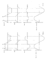
- circuit diagrams of Figures 1 and 2 represent a selfconfiguring, double bridge amplifier, for example for a stereo channel of an audio reproduction installation.
- the gist of this invention will be better illustrated by first analyzing a circuit without disturbances suppressing means (Fig. 1, Fig. 3a) and thereafter with disturbances suppressing means (Fig. 2, Fig. 3b).
- each common mode control loop comprises a resistive voltage divider RC1-RC2 (RC3-RC4), a common mode differential amplifier Gm1 (Gm2) and a configuring switch SW_CL1 (SW_CL2).
- the common mode feedback amplifiers Gm1 and Gm2 are practically disactivated by their respective configuring switches SW_CL1 and SW_CL2 which shortcircuit the input terminals of the respective feedback amplifier.
- the configuring window comparator When, upon the rise of the input signal level, the configuring window comparator commands the configuring switches to implement a double bridge structure, that is with SW_F closed and SW_C open, the relative switches SW_CL1 and SW_CL2 switch to ground potential.
- each common mode amplifier acts on the respective pair of operational amplifiers OPA+F and OPA-F which compose a single bridge driving a respective load (loudspeaker), so as to bring the voltage (Vc1) of the common node of the resistances RC1 and RC2 to ground potential.
- Vc1 the common node of the resistances RC1 and RC2
- FIG. 3a it may be observed that these transitions of the inverting input of the common mode feedback amplifier cause abrupt voltage variations on the outputs of the amplifiers (instants labelled A, B, C and D in the diagrams) when the node Vc1 switches from a certain potential assumed before the switching to ground potential.
- these abrupt voltage changes may be avoided by modifying the manner in which the selfconfiguring system operates (enables and disables the relative common mode control loop) and precisely by storing the actual voltage of the common mode control node (Vc1), assumed during a phase in which the common mode control loop is disactivated, that is when the two inputs of the common mode feedback amplifier (Gm1) are shortcircuited, on a storage capacitor connected between the inverting input of the feedback amplifier at ground. In this way, the opening and closing of the input shortcircuiting switch will not generate any abrupt voltage change at these input nodes.
- the system of the invention may be fully implemented as depicted in Fig. 2 by introducing a storage capacitor CM1 (CM2) that may be connected (as shown in the example of Fig. 2) between the inverting input of the common mode feedback differential amplifier Gm1 (Gm2) and ground, and by employing a simple configuring switch SW_CL1 (SW_CL2) for shortcircuiting the inverting input with the noninverting input of the common mode feedback amplifier when the selfconfiguring system commands a bridge configuration of the pair of amplifiers OPA+F and OPA-F (OPA-R and OPA+R).
- CM1 storage capacitor
- SW_CL1 simple configuring switch
- CM1 CM2
- SW_CL1 the relative configuring switch SW_CL1
- Gm1 Gm2
- the capacitor stores the common output node Vc1 (Vc2) during a closing phase of the configuring switch.
- any pair of bridge configurable amplifiers for example to the pair composed of OPA+F and OPA-F
- the storage capacitor Cm1 charges to the voltage of the common mode control node Vc1, which corresponds to the intermediate node of the resistive voltage divider composed of the resistances RC1 and RC2 of the common mode control network.
- the storage capacitor Cm1 retains this voltage information for the whole period during which the configuring switch SW_CL1 remains open and therefore acts on the common mode control loop so as to maintain the potential of the common mode control node Vc1 at the same value it had at the switching instant.
- the system of the invention eliminates any abrupt changes of the output voltages in correspondence of the switching instants A, B, C and D.
- the device of the invention can be easily realized because the value of the storage capacitance Cm1 may be very small and therefore can be easily integrated.
- the coupling of the output of the common mode feedback differential amplifier to the respective configurable amplifier of the pair of amplifiers may be implemented in various ways.
- a particularly effective embodiment is shown in the partial circuit of Fig. 4.
- the resistances, R2 and R3 respectively, of the feedback loop of the operational amplifier OPA+F of one pair of amplifiers, which can be configured to function in a single ended mode of the functional diagram of Fig. 2, may be subdivided by employing pairs of resistances R2-R2' and R3-R3', as shown in Fig. 4.
- the common node of the resistances R2' and R3' which is connected to the inverting input of the OPA+F operational amplifier, is also connected to the output of the common mode feedback amplifier Gm1.
- the ability of retaining the voltage information of the storage capacitor Cm1, which must necessarily require a small area of integration and therefore has a relatively small capacitance, may be enhanced by minimizing the input currents of the common mode feedback amplifier Gm1.
- field effect input transistors MOSFET
- a suitable common mode differential feedback amplifier circuit is schematically shown in Fig. 5.
Landscapes
- Engineering & Computer Science (AREA)
- Power Engineering (AREA)
- Amplifiers (AREA)
Claims (5)
- Circuit de contrôle en modalité commune pour un couple d'amplificateurs (OPA+F_OPA-F, OPA+R_OPA-R) autoconfigurants dans une configuration à pont pour piloter une première charge et dans une modalité de fonctionnement à une seule extrémité de l'un des dits amplificateurs(OPA+F ; OPA-R) pour piloter la dite première charge, en fonction du niveau d'un signal d'entrée (IN-F ; IN-R), comprenant au moins un amplificateur différentiel de rétroaction en modalité commune (Gm1, Gm2) ayant une entrée non invertissant (+) reliée à un noeud de contrôle de modalité commune (Vc1, Vc2) dudit couple (OPA+F_OPA-F, OPA+R_OPA-R) d'amplificateurs et une entrée invertissant (-) qui est commutée par des moyens de configuration,
caractérisé en ce qu'il comprendun interrupteur de configuration (SW_CL1, SW_CL2) qui met en court-circuit la dite entrée invertissant avec la dite entrée non invertissant ;un condensateur de mémorisation (CM1, CM2) relié entre l'une quelconque des dites deux entrées (+, -) et un noeud commun de potentiel du circuit des amplificateurs. - Circuit de contrôle en modalité commune comme il est défini dans la revendication 1, dans lequel le dit amplificateur différentiel de réaction en modalité commune (Gm1, Gm2) comprend un couple de transistors d'entrée à effet de champ.
- est défini dans la revendication 1, dans lequel le dit condensateur de mémorisation (CM1, CM2) est relié à l'entrée invertissant (-) dudit amplificateur en modalité commune.
- Circuit de contrôle en modalité commune comme il est défini dans la revendication 1, dans lequel le dit premier amplificateur (OPA+F) du couple (OPA+F ; OPA-F) est configuré dans une modalité de fonctionnement à une seule extrémité pour piloter dans une modalité à pont la dite première charge en série avec une deuxième charge d'un couple similaire d'amplificateurs autoconfigurants (OPA+R_OPA-R) en fonction du niveau d'au moins un des signaux d'entrée (IN-F ; IN-R).
- Méthode pour prévenir des changements brusques de tension aux sorties d'un couple d'amplificateurs (OPA+F_OPA-F, OPA+R_OPA-R) autoconfigurants dans une configuration à pont pour piloter une première charge et dans une modalité de fonctionnement à une seule extrémité de l'un des dits amplificateurs(OPA+F; OPA-R) ) pour piloter la dite première charge, en fonction du niveau d'un signal d'entrée (IN-F ; IN-R) le dit couple d'amplificateurs, fournissant au moins un amplificateur différentiel de réaction en modalité commune (Gm1, Gm2) ayant une fonctionnalité d'entrée non invertissant (+)(+) reliée à un noeud de contrôle de modalité commune (Vc1, Vc2) de le dit couple d'amplificateurs et une entrée invertissant (-) qui est commutée par des moyens de configuration,
caractérisé parla mémorisation de la tension de modalité commune émise par le dit couple d'amplificateurs sur un condensateur(CM1, CM2) relié entre une entrée (+, -) du dit amplificateur différentiel de réaction en modalité commune (Gm1, Gm2) et un noeud commun de potentiel du circuit des amplificateurs, pendant une phase configuration à pont quand les dites entrées(+, -) sont court-circuitées par un interrupteur de configuration (SW_CL1, SW_CL2) ;l'exploitation de l'information de tension mémorisée dans le dit condensateur(CM1, CM2) pou maintenir constante la tension sur le dit noeud de contrôle de modalité commune (Vc1, Vc2), pendant une phase de configuration à une seule extrémité quand le dit interrupteur de mise en court circuit (SW_CL1, SW_CL2) est ouvert.
Priority Applications (4)
| Application Number | Priority Date | Filing Date | Title |
|---|---|---|---|
| DE69429660T DE69429660T2 (de) | 1994-10-07 | 1994-10-07 | Brückenverstärker mit hohem Wirkungsgrad |
| EP94830478A EP0706260B1 (fr) | 1994-10-07 | 1994-10-07 | Amplificateur de pont à grande efficacité |
| US08/540,401 US5654668A (en) | 1994-10-07 | 1995-10-06 | High efficiency bridge amplifier |
| JP28785395A JP3593192B2 (ja) | 1994-10-07 | 1995-10-09 | 高効率ブリッジ増幅器 |
Applications Claiming Priority (1)
| Application Number | Priority Date | Filing Date | Title |
|---|---|---|---|
| EP94830478A EP0706260B1 (fr) | 1994-10-07 | 1994-10-07 | Amplificateur de pont à grande efficacité |
Publications (2)
| Publication Number | Publication Date |
|---|---|
| EP0706260A1 EP0706260A1 (fr) | 1996-04-10 |
| EP0706260B1 true EP0706260B1 (fr) | 2002-01-16 |
Family
ID=8218551
Family Applications (1)
| Application Number | Title | Priority Date | Filing Date |
|---|---|---|---|
| EP94830478A Expired - Lifetime EP0706260B1 (fr) | 1994-10-07 | 1994-10-07 | Amplificateur de pont à grande efficacité |
Country Status (4)
| Country | Link |
|---|---|
| US (1) | US5654668A (fr) |
| EP (1) | EP0706260B1 (fr) |
| JP (1) | JP3593192B2 (fr) |
| DE (1) | DE69429660T2 (fr) |
Families Citing this family (14)
| Publication number | Priority date | Publication date | Assignee | Title |
|---|---|---|---|---|
| JP3881448B2 (ja) * | 1998-03-31 | 2007-02-14 | 株式会社東芝 | 電力増幅回路 |
| IT1305650B1 (it) * | 1998-12-16 | 2001-05-15 | St Microelectronics Srl | Circuito per assicurare una completa saturazione di entrambi gliamplificatori di un amplificatore a ponte configurato ad ingresso |
| US7167569B1 (en) * | 2000-10-25 | 2007-01-23 | National Semiconductor Corporation | Output coupling capacitor free audio power amplifier dynamically configured for speakers and headphones with excellent click and pop performance |
| US6552607B1 (en) * | 2001-11-12 | 2003-04-22 | Apogee Technology Inc. | Time division multiplexed PWM amplifier |
| DE60317806T2 (de) * | 2003-12-23 | 2008-10-30 | Stmicroelectronics S.R.L., Agrate Brianza | Verfahren zum Verhindern abrupter Spannungsänderungen am Ausgang eines Verstärkerpaars und Regelschaltung für ein selbstkonfigurierendes Verstärkerpaar in einer Brückenkonfiguration |
| WO2005069484A1 (fr) * | 2004-01-07 | 2005-07-28 | Koninklijke Philips Electronics N.V. | Circuit amplificateur configurable |
| US9300261B2 (en) * | 2006-03-10 | 2016-03-29 | Nvidia Corporation | Method and apparatus for efficient load biasing |
| US7548178B2 (en) * | 2006-03-10 | 2009-06-16 | Nvidia Corporation | Method and apparatus for ADC size and performance optimization |
| US7760015B2 (en) * | 2008-03-13 | 2010-07-20 | Exar Corporation | Combination offset voltage and bias current auto-zero circuit |
| US7907008B2 (en) * | 2008-12-30 | 2011-03-15 | Intel Corporation | Dynamic signal contamination suppression |
| EP2802076B1 (fr) * | 2013-05-08 | 2015-11-18 | Nxp B.V. | Configuration d'amplificateur à double pont |
| US10601423B2 (en) | 2013-11-28 | 2020-03-24 | Nxp Usa, Inc. | Low-voltage differential signaling (differential signaling) driver circuit and method of enabling and disabling a differential signaling driver circuit |
| JP6360453B2 (ja) | 2015-03-16 | 2018-07-18 | 株式会社東芝 | 電力増幅装置 |
| CN113783532B (zh) * | 2020-06-10 | 2025-02-07 | 武汉杰开科技有限公司 | 一种功率放大器及其控制方法、车载音频系统 |
Family Cites Families (5)
| Publication number | Priority date | Publication date | Assignee | Title |
|---|---|---|---|---|
| DE2527904C3 (de) * | 1975-06-23 | 1980-07-17 | Licentia Patent-Verwaltungs-Gmbh, 6000 Frankfurt | Schaltungsanordnung zur galvanischen Ankopplung einer Last an zwei gleichstromgekoppelte Verstärker |
| US4494077A (en) * | 1981-12-02 | 1985-01-15 | Nippon Electric Co., Ltd. | Amplifier system switchable between two amplifying operations |
| IT1229860B (it) * | 1988-11-09 | 1991-09-13 | Sgs Thomson Microelectronics | Amplificatore audio integrato con regolazione unificata delle funzioni di "mute" e "stand by" e dei transitori di commutazione. |
| IT1243920B (it) * | 1990-11-20 | 1994-06-28 | Sgs Thomson Microelectronics | Amplificatore audio di potenza ad alta efficienza composto da due amplificatori con unica alimentazione. |
| DE69314933T2 (de) * | 1993-02-24 | 1998-06-10 | St Microelectronics Srl | Selbstkonfigurierbarer Doppelbrückenverstärker |
-
1994
- 1994-10-07 DE DE69429660T patent/DE69429660T2/de not_active Expired - Fee Related
- 1994-10-07 EP EP94830478A patent/EP0706260B1/fr not_active Expired - Lifetime
-
1995
- 1995-10-06 US US08/540,401 patent/US5654668A/en not_active Expired - Lifetime
- 1995-10-09 JP JP28785395A patent/JP3593192B2/ja not_active Expired - Fee Related
Also Published As
| Publication number | Publication date |
|---|---|
| JP3593192B2 (ja) | 2004-11-24 |
| DE69429660D1 (de) | 2002-02-21 |
| EP0706260A1 (fr) | 1996-04-10 |
| JPH08213858A (ja) | 1996-08-20 |
| US5654668A (en) | 1997-08-05 |
| DE69429660T2 (de) | 2002-11-14 |
Similar Documents
| Publication | Publication Date | Title |
|---|---|---|
| EP0706260B1 (fr) | Amplificateur de pont à grande efficacité | |
| US5982231A (en) | Multiple channel class D audio amplifier | |
| JP3459109B2 (ja) | 自己構成可能な二元的ブリッジパワー増幅器 | |
| EP1456942B1 (fr) | Amplificateur a modulation d'impulsions en duree a multiplexage a repartition dans le temps | |
| US20080024213A1 (en) | Amplifier circuits, methods of starting and stopping amplifier circuits | |
| US20090102556A1 (en) | Class d amplifier | |
| JPH04357704A (ja) | 単一の供給源を持つ2つの増幅器を含む高効率電力オーディオ増幅器 | |
| WO2010067823A1 (fr) | Amplificateur électrique classe d | |
| US8687821B2 (en) | Plop-free amplifier | |
| EP1548933B1 (fr) | Méthode pour la prévention des variations de tension abruptes à la sortie d'une paire de circuits d'amplificateur et circuit de régulation pour une paire de circuits d'amplificateur à autoconfiguration dans une configuration en pont | |
| US7167047B2 (en) | Multi-channel power amplifier self-configuring to a bridge or single-ended output, particularly for audio applications | |
| KR20040094180A (ko) | 신호 발생장치 및 신호 발생방법 | |
| JP2003318656A (ja) | ショック音防止回路 | |
| US4827221A (en) | Integrated audio amplifier commutable in a bridge or stereo configuration in a seven pin package | |
| US6967527B2 (en) | Pulse width modulation amplifier | |
| EP0927453A1 (fr) | Procede et appareil de sortie a trois etats, destines a des amplificateurs a haute vitesse | |
| KR100453708B1 (ko) | 고효율 스위칭 증폭기 | |
| US4668921A (en) | Power supply circuit | |
| JP3057655B2 (ja) | 磁気記録再生装置 | |
| US20030184376A1 (en) | Class D amplifier energy control | |
| JP3332219B2 (ja) | 音場拡大装置 | |
| JPS61112408A (ja) | 電力増幅器 | |
| JPH06152268A (ja) | スイッチングアンプ | |
| JPH0451706A (ja) | 切換増幅器 | |
| JPH0668406A (ja) | 再生増幅回路 |
Legal Events
| Date | Code | Title | Description |
|---|---|---|---|
| PUAI | Public reference made under article 153(3) epc to a published international application that has entered the european phase |
Free format text: ORIGINAL CODE: 0009012 |
|
| AK | Designated contracting states |
Kind code of ref document: A1 Designated state(s): DE FR GB IT |
|
| 17P | Request for examination filed |
Effective date: 19960527 |
|
| RAP3 | Party data changed (applicant data changed or rights of an application transferred) |
Owner name: STMICROELECTRONICS S.R.L. |
|
| 17Q | First examination report despatched |
Effective date: 19990112 |
|
| GRAG | Despatch of communication of intention to grant |
Free format text: ORIGINAL CODE: EPIDOS AGRA |
|
| GRAH | Despatch of communication of intention to grant a patent |
Free format text: ORIGINAL CODE: EPIDOS IGRA |
|
| GRAH | Despatch of communication of intention to grant a patent |
Free format text: ORIGINAL CODE: EPIDOS IGRA |
|
| GRAA | (expected) grant |
Free format text: ORIGINAL CODE: 0009210 |
|
| REG | Reference to a national code |
Ref country code: GB Ref legal event code: IF02 |
|
| AK | Designated contracting states |
Kind code of ref document: B1 Designated state(s): DE FR GB IT |
|
| PG25 | Lapsed in a contracting state [announced via postgrant information from national office to epo] |
Ref country code: FR Free format text: LAPSE BECAUSE OF FAILURE TO SUBMIT A TRANSLATION OF THE DESCRIPTION OR TO PAY THE FEE WITHIN THE PRESCRIBED TIME-LIMIT Effective date: 20020116 |
|
| REF | Corresponds to: |
Ref document number: 69429660 Country of ref document: DE Date of ref document: 20020221 |
|
| EN | Fr: translation not filed | ||
| PLBE | No opposition filed within time limit |
Free format text: ORIGINAL CODE: 0009261 |
|
| STAA | Information on the status of an ep patent application or granted ep patent |
Free format text: STATUS: NO OPPOSITION FILED WITHIN TIME LIMIT |
|
| 26N | No opposition filed | ||
| PGFP | Annual fee paid to national office [announced via postgrant information from national office to epo] |
Ref country code: DE Payment date: 20040924 Year of fee payment: 11 |
|
| PG25 | Lapsed in a contracting state [announced via postgrant information from national office to epo] |
Ref country code: IT Free format text: LAPSE BECAUSE OF NON-PAYMENT OF DUE FEES Effective date: 20051007 |
|
| PG25 | Lapsed in a contracting state [announced via postgrant information from national office to epo] |
Ref country code: DE Free format text: LAPSE BECAUSE OF NON-PAYMENT OF DUE FEES Effective date: 20060503 |
|
| PGFP | Annual fee paid to national office [announced via postgrant information from national office to epo] |
Ref country code: GB Payment date: 20110926 Year of fee payment: 18 |
|
| GBPC | Gb: european patent ceased through non-payment of renewal fee |
Effective date: 20121007 |
|
| PG25 | Lapsed in a contracting state [announced via postgrant information from national office to epo] |
Ref country code: GB Free format text: LAPSE BECAUSE OF NON-PAYMENT OF DUE FEES Effective date: 20121007 |