EP0706288A2 - Circuit de correction dépendant du gain à haute résolution - Google Patents
Circuit de correction dépendant du gain à haute résolution Download PDFInfo
- Publication number
- EP0706288A2 EP0706288A2 EP95114903A EP95114903A EP0706288A2 EP 0706288 A2 EP0706288 A2 EP 0706288A2 EP 95114903 A EP95114903 A EP 95114903A EP 95114903 A EP95114903 A EP 95114903A EP 0706288 A2 EP0706288 A2 EP 0706288A2
- Authority
- EP
- European Patent Office
- Prior art keywords
- circuit
- ref
- digital
- signal
- input signal
- Prior art date
- Legal status (The legal status is an assumption and is not a legal conclusion. Google has not performed a legal analysis and makes no representation as to the accuracy of the status listed.)
- Withdrawn
Links
Images
Classifications
-
- H—ELECTRICITY
- H04—ELECTRIC COMMUNICATION TECHNIQUE
- H04N—PICTORIAL COMMUNICATION, e.g. TELEVISION
- H04N25/00—Circuitry of solid-state image sensors [SSIS]; Control thereof
- H04N25/60—Noise processing, e.g. detecting, correcting, reducing or removing noise
- H04N25/67—Noise processing, e.g. detecting, correcting, reducing or removing noise applied to fixed-pattern noise, e.g. non-uniformity of response
- H04N25/671—Noise processing, e.g. detecting, correcting, reducing or removing noise applied to fixed-pattern noise, e.g. non-uniformity of response for non-uniformity detection or correction
-
- H—ELECTRICITY
- H04—ELECTRIC COMMUNICATION TECHNIQUE
- H04N—PICTORIAL COMMUNICATION, e.g. TELEVISION
- H04N1/00—Scanning, transmission or reproduction of documents or the like, e.g. facsimile transmission; Details thereof
- H04N1/40—Picture signal circuits
- H04N1/401—Compensating positionally unequal response of the pick-up or reproducing head
Definitions
- the present invention relates to signal processing circuits and systems. More specifically, the present invention relates to circuits and systems for providing automatic gain and offset control.
- Night vision systems are well known in the art. Night vision systems typically include a cryogenically cooled linear detector array with an associated cryogenic subsystem, a scanning system which moves a image across a two-dimensional array, and a refractive optical system which focuses energy onto the detector.
- the detectors in the array either sense the heat of a body or detect low light levels.
- the rage of gain adjustments required across one array may differ considerably from the range of adjustments required across another array. That is, gain correction across one array might vary from .5 to 1.5, while the gain correction variation across another array may vary from .9 to 1.1.
- one array may require the full dynamic range of the DAC, while another may require only a portion of same. This leads to an underutilization of the dynamic range of the DAC for certain arrays and an associated suboptimum performance.
- Digital-to-analog converters are typically expensive devices relative to other components in the system and these devices often set the dominant parameters of system performance. Full utilization of the dynamic range of a DAC allows a full utilization of the resolution of the device.
- correction resolution means the extent to which the device can discriminate between input signals that are close in amplitude or digital code and provide corresponding output signals which are widely spaced.
- the need in the art is addressed by the present invention which provides a high resolution gain response correction circuit.
- the inventive circuit is adapted for use with a first circuit for providing a first analog input signal and includes a second circuit for providing a second input signal in response to the first input signal.
- a third circuit is included for providing an analog output signal in response to the first and second input signals.
- the third circuit is a digital-to-analog converter.
- the digital-to analog-converter is adapted to adjust the output signal level in response to an individual pixel correction reference signal.
- a digital potentiometer allows for the first input signal to be scaled and used to adjust the level of the second input signal. By adjusting the setting of the potentiometer, the dynamic range of the output of the DAC may be adjusted.
- the inventive arrangement allows for the gain correction range of a digital-to-analog converter to be matched to a particular array under test via software control.
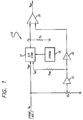
- Fig. 1 is a block diagram of an illustrative implementation of the gain correction circuit of the present invention.
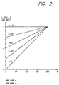
- Fig. 2 is a graph of a family of lines showing the transfer function of the DAC as a function of the fractional setting of the range scale potentiometer (y) and the pixel correction value (n).
- Fig. 1 is a block diagram of an illustrative implementation of the gain correction circuit of the present invention.
- the inventive circuit 10 includes a conventional digital-to-analog converter 12 which receives a first analog input signal (V in ) from a circuit such as an automatic gain control circuit (not shown).
- V in is the voltage representing global gain as required by the automatic gain control loop.
- the first input signal V in is supplied to a first terminal of a conventional digital potentiometer.
- the second terminal of the digital potentiometer is connected to ground.
- the output terminal of the digital potentiometer is connected to a unity gain buffer ampliflier 16.
- the setting on the wiper of the potentiometer may be set under software control.
- the output of the unity gain amplifier 16 is connected to a first terminal of a resistor R ref .
- the second terminal of the resistor R ref is connected to a second input terminal of the DAC 12.
- a digital pixel correction signal is provided to the DAC by a memory such as an electrically erasible programmable read-only memory (EPROM).
- EPROM electrically erasible programmable read-only memory
- the output of the DAC is a first input to a differential amplifier 20.
- the DAC output signal is developed across an output resistor R o which has its second terminal connected to ground.
- a second input to the differential amplifier 20 is provided by the output of an inverter 22.
- the inverter 22 receives input from the output of the buffer amplifier 16.
- R ref is not connected to ground.
- I ref is less than V ref /R ref .
- V o is reduced by a factor "y" which is the fractional setting of the range scale potentiometer R p .
- the parameter "y" represents the lower limit of the gain control range and is a number between zero and one.
- the voltage at the second terminal of the DAC 12 is equal to the voltage across the resistor R ref added to the voltage at the other end of the resistor.
- the voltage across the resistor R ref is equal to the net current flowing through the resistor (I ref ) times the resistance of the resistor (R ref ).
- the DAC 12 will adjust current out of the second terminal as necessary to make the voltages at the input terminals equal.
- the current through the resistor I ref is reduced from V o /R ref (in the case where R ref is returned to ground) by an amount (y times V ref /R ref ) which represents the extent to which the input voltage at the second terminal is scaled down by the range scale potentiometer.
- Fig. 2 is a graph of a family of lines showing the transfer function of the DAC 12 as a function of the fractional setting of the range scale potentiometer (y) and the pixel correction value (n). Note that the maximum gain is unity and the minimum gain is y.
Landscapes
- Engineering & Computer Science (AREA)
- Multimedia (AREA)
- Signal Processing (AREA)
- Analogue/Digital Conversion (AREA)
Applications Claiming Priority (2)
| Application Number | Priority Date | Filing Date | Title |
|---|---|---|---|
| US319382 | 1989-03-03 | ||
| US08/319,382 US5517192A (en) | 1994-10-05 | 1994-10-05 | High resolution gain response correction circuit |
Publications (2)
| Publication Number | Publication Date |
|---|---|
| EP0706288A2 true EP0706288A2 (fr) | 1996-04-10 |
| EP0706288A3 EP0706288A3 (fr) | 1998-09-16 |
Family
ID=23242026
Family Applications (1)
| Application Number | Title | Priority Date | Filing Date |
|---|---|---|---|
| EP95114903A Withdrawn EP0706288A3 (fr) | 1994-10-05 | 1995-09-21 | Circuit de correction dépendant du gain à haute résolution |
Country Status (3)
| Country | Link |
|---|---|
| US (1) | US5517192A (fr) |
| EP (1) | EP0706288A3 (fr) |
| IL (1) | IL115526A0 (fr) |
Families Citing this family (2)
| Publication number | Priority date | Publication date | Assignee | Title |
|---|---|---|---|---|
| JP2002236152A (ja) * | 2001-02-08 | 2002-08-23 | Mitsubishi Electric Corp | 半導体集積回路の試験装置及び試験方法 |
| US20070299895A1 (en) * | 2006-06-09 | 2007-12-27 | Johnson Scot L | System and method of generating electrical stimulation waveforms as a therapeutic modality |
Family Cites Families (6)
| Publication number | Priority date | Publication date | Assignee | Title |
|---|---|---|---|---|
| US4806914A (en) * | 1987-05-07 | 1989-02-21 | General Electric Company | Detection by automatic gain control features of gradual cutting tool breakage |
| US4891645A (en) * | 1988-10-04 | 1990-01-02 | Analog Devices Inc. | Digital-to-analog converter with on-board unity gain inverting amplifier |
| FR2652471B1 (fr) * | 1989-09-22 | 1991-11-29 | Thomson Csf | Dispositif de correction des defauts d'une suite d'images analysee par un capteur infrarouge matriciel a integration. |
| DE4130338A1 (de) * | 1991-09-12 | 1993-03-18 | Thomson Brandt Gmbh | Schaltung mit einem a/d-wandler- oder d/a-wandler |
| JPH05307833A (ja) * | 1992-05-01 | 1993-11-19 | Funai Denki Kenkyusho:Kk | 圧縮・伸張回路 |
| US5381148A (en) * | 1993-07-12 | 1995-01-10 | Analog Devices, Inc. | Method and apparatus for calibrating a gain control circuit |
-
1994
- 1994-10-05 US US08/319,382 patent/US5517192A/en not_active Expired - Fee Related
-
1995
- 1995-09-21 EP EP95114903A patent/EP0706288A3/fr not_active Withdrawn
- 1995-10-05 IL IL11552695A patent/IL115526A0/xx unknown
Non-Patent Citations (1)
| Title |
|---|
| None |
Also Published As
| Publication number | Publication date |
|---|---|
| EP0706288A3 (fr) | 1998-09-16 |
| IL115526A0 (en) | 1996-01-19 |
| US5517192A (en) | 1996-05-14 |
Similar Documents
| Publication | Publication Date | Title |
|---|---|---|
| US6274869B1 (en) | Digital offset corrector | |
| US6538250B2 (en) | Microbolometer focal plane array with controlled bias | |
| US6249002B1 (en) | Bolometric focal plane array | |
| US7105818B2 (en) | Microbolometer focal plane array with temperature compensated bias | |
| US6730909B2 (en) | Methods and apparatus for compensating a radiation sensor for temperature variations of the sensor | |
| EP0773669B1 (fr) | Circuit, élément d'image, dispositif et méthode pour la réduction du motif de bruit fixe dans des dispositifs de prise d'images à l'état solide | |
| US5953060A (en) | Method for reducing fixed pattern noise in solid state imaging devices | |
| US6359460B1 (en) | Semiconductor memory device | |
| KR0173827B1 (ko) | 열 적외선 카메라용 아날로그 신호 처리 회로 | |
| US6762398B1 (en) | Imaging device with fixed-pattern-noise correction regulated constant-current source | |
| US6642496B1 (en) | Two dimensional optical shading gain compensation for imaging sensors | |
| US6683310B2 (en) | Readout technique for microbolometer array | |
| EP1366344B1 (fr) | Procede et appareil de lecture d'un reseau de bolometres au moyen de plusieurs impulsions polarisees | |
| JP3809653B2 (ja) | プログラミング可能なオフセット電流を有する光検知装置 | |
| EP0835586A2 (fr) | Correcteur numerique de decalage pour matrice de microbolometres | |
| EP0706288A2 (fr) | Circuit de correction dépendant du gain à haute résolution | |
| JP2002044370A (ja) | イメージセンサ | |
| EP0870330B1 (fr) | Detecteur matriciel bolometrique | |
| Broekaert et al. | Nonlinearity and nonuniformity corrections for the IRIS family of IRCCD thermal imagers | |
| JP3377000B2 (ja) | 半導体装置 | |
| Tanaka et al. | A non-uniformity correction scheme using multiple analog buses for an uncooled infrared sensor | |
| GB2250089A (en) | Spectrometer | |
| JPH07105663B2 (ja) | 増幅装置 | |
| JP3582034B2 (ja) | 赤外線撮像装置の増幅装置 | |
| EP0904656A1 (fr) | Annulation de capacite dans le groupement focal |
Legal Events
| Date | Code | Title | Description |
|---|---|---|---|
| PUAI | Public reference made under article 153(3) epc to a published international application that has entered the european phase |
Free format text: ORIGINAL CODE: 0009012 |
|
| AK | Designated contracting states |
Kind code of ref document: A2 Designated state(s): DE ES FR GB |
|
| PUAL | Search report despatched |
Free format text: ORIGINAL CODE: 0009013 |
|
| STAA | Information on the status of an ep patent application or granted ep patent |
Free format text: STATUS: THE APPLICATION IS DEEMED TO BE WITHDRAWN |
|
| AK | Designated contracting states |
Kind code of ref document: A3 Designated state(s): DE ES FR GB |
|
| 18D | Application deemed to be withdrawn |
Effective date: 19980331 |