EP0706854B1 - Scheibenhalter für Halbleiterscheiben-Poliermaschine - Google Patents
Scheibenhalter für Halbleiterscheiben-Poliermaschine Download PDFInfo
- Publication number
- EP0706854B1 EP0706854B1 EP95307173A EP95307173A EP0706854B1 EP 0706854 B1 EP0706854 B1 EP 0706854B1 EP 95307173 A EP95307173 A EP 95307173A EP 95307173 A EP95307173 A EP 95307173A EP 0706854 B1 EP0706854 B1 EP 0706854B1
- Authority
- EP
- European Patent Office
- Prior art keywords
- wafer
- chuck
- joint
- semi
- polishing
- Prior art date
- Legal status (The legal status is an assumption and is not a legal conclusion. Google has not performed a legal analysis and makes no representation as to the accuracy of the status listed.)
- Expired - Lifetime
Links
- 238000005498 polishing Methods 0.000 title claims abstract description 64
- 239000004065 semiconductor Substances 0.000 title claims abstract description 24
- 230000002093 peripheral effect Effects 0.000 claims description 15
- 230000000717 retained effect Effects 0.000 claims description 2
- 239000000463 material Substances 0.000 abstract description 7
- 235000012431 wafers Nutrition 0.000 description 81
- 230000008878 coupling Effects 0.000 description 7
- 238000010168 coupling process Methods 0.000 description 7
- 238000005859 coupling reaction Methods 0.000 description 7
- 239000002002 slurry Substances 0.000 description 4
- 239000000126 substance Substances 0.000 description 3
- 238000011109 contamination Methods 0.000 description 2
- 239000004677 Nylon Substances 0.000 description 1
- 230000003466 anti-cipated effect Effects 0.000 description 1
- 229910052790 beryllium Inorganic materials 0.000 description 1
- 230000000295 complement effect Effects 0.000 description 1
- 238000010276 construction Methods 0.000 description 1
- 230000002706 hydrostatic effect Effects 0.000 description 1
- 230000013011 mating Effects 0.000 description 1
- 238000012986 modification Methods 0.000 description 1
- 230000004048 modification Effects 0.000 description 1
- 229920001778 nylon Polymers 0.000 description 1
- 229910001220 stainless steel Inorganic materials 0.000 description 1
- 239000010935 stainless steel Substances 0.000 description 1
Images



Classifications
-
- B—PERFORMING OPERATIONS; TRANSPORTING
- B24—GRINDING; POLISHING
- B24B—MACHINES, DEVICES, OR PROCESSES FOR GRINDING OR POLISHING; DRESSING OR CONDITIONING OF ABRADING SURFACES; FEEDING OF GRINDING, POLISHING, OR LAPPING AGENTS
- B24B37/00—Lapping machines or devices; Accessories
- B24B37/27—Work carriers
- B24B37/30—Work carriers for single side lapping of plane surfaces
Definitions
- This invention relates to chemical mechanical wafer polishing machines of the type used to planarize semi-conductor wafers, and in particular to an improved wafer holder for supporting a wafer in such a polishing machine.
- Baldy U.S. Patent 5,297,361 discloses a wafer polishing machine with a sample holding table that includes a cardan joint.
- the wafer being polished is supported on an inner ring that is mounted for rotation about a first rotational axis on an outer ring.
- the outer ring is in turn mounted for rotation with respect to a support about a second rotational axis.
- the first and second rotational axes are perpendicular, and they intersect at the center of the sample face to be polished.
- Baldy addresses the problem that conventional wafer holders often tend to remove material from the periphery of the wafer at a faster rate than the center of the wafer. This can be a serious problem, which is only exacerbated by rotation of the wafer holder, which also tends to remove material at a faster rate from the periphery of the wafer.
- the wafer holder of Baldy includes elements of the cardan joint that project beyond the polishing plane of the wafer. This arrangement provides significant disadvantages, particularly in systems having a polishing pad which is larger in area than the wafer being polished.
- EP 0362811 discloses a polishing apparatus including a wafer holder with a pressure applying means which applies air pressure either to a centre portion of a wafer to be polished or to the entire rear surface of the wafer.
- EP 0284343 discloses a counterbalanced polishing apparatus including a force transmitting member which is connected such that pressure is directed to a portion of a chuck closer to its periphery than to its centre. However, force is distributed asymmetrically because the force transmitting member only partially contacts the chuck at a point away from its central region.
- EP 0589433 which is regarded on the closest prior art, discloses a semi-conductor wafer polishing machine for polishing a wafer having a surface to be polished that defines a polishing plane, said machine comprising at least one polishing pad assembly and at least one wafer holder positioned to hold a semi-conductor wafer against the polishing pad assembly, said wafer holder comprising a joint for supporting a wafer chuck, the joint allowing rotation about at least two axes, which axes are parallel to the plane of the wafer and intersect at a centre of rotation,
- FR-E-96278 discloses an apparatus having a cardan joint comprising a housing, an outer ring mounted on the housing by two first bearings aligned with a first axis of rotation, an inner ring rotatably mounted on the outer ring by two second bearings aligned with a second axis of rotation.
- the present invention relates to a semi-conductor wafer polishing machines as claimed in claim 1 and claim 10, the machines of the type comprising at least one polishing pad assembly and at least one wafer holder positioned to hold a semi-conductor wafer against the polishing pad assembly.
- the wafer holder comprises a wafer chuck and a chuck support element.
- the wafer chuck is configured to support the wafer and comprises a center and a periphery.
- the wafer chuck is coupled to the chuck support at a coupling region located closer to the periphery than to the center such that forces applied to the chuck by the chuck support element stress a peripheral portion of the chuck to a greater extent than a central portion of the chuck.
- FIG. 1 is a schematic view of a polishing machine 10 that incorporates a presently preferred embodiment of this invention.
- This polishing machine 10 includes a polishing pad assembly 12 including a polishing pad belt 14 and a belt platen 16.
- a wafer holder 18 holds a semi-conductor wafer W to be polished, with a polished surface of the wafer W positioned against the polishing pad belt 14.
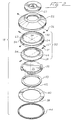
- the wafer holder 18 includes a cardan joint 20 supported in an outer housing 22.
- the cardan joint 20 includes an outer ring 24 that is mounted for rotation with respect to the housing 22 by two first bearings 26 and first shafts 27 that are aligned with the X axis in this embodiment.
- An inner ring 28 is mounted for rotation with respect to the outer ring 24 by two second bearings 30 and second shafts 31 that are aligned with the Y axis in this embodiment.
- the X and Y axes meet at a central position in the wafer holder 18 and define a center of rotation 34.
- a wafer chuck 32 is supported only around its periphery by the inner ring 28.
- the wafer chuck 32 can be formed in any suitable manner so as to hold the wafer W in place on the chuck 32 during polishing. In some cases, the wafer chuck 32 may include vacuum hold-down devices to secure the wafer W on the wafer chuck 32, though such hold-down devices are not always required.
- the exposed surface of the wafer W that is positioned adjacent the polishing pad belt 14 defines a polishing plane 36 ( Figure 1).
- the cardan joint 20 is provided with an annular elastomeric seal 38.
- the inner periphery 40 of the seal 38 fits within a peripheral groove 42 of the guide ring 33 and is retained therein.
- the outer periphery of the seal 38 is releasably secured to the housing 22 by a clamp ring 44 that is held in place, for example by nylon screws.
- the seal 38 prevents the slurry used in the chemical mechanical polishing operation from entering the interior of the cardan joint 20.
- the seal 38 has sufficient flexibility to allow the outer and inner rings 24, 28 to rotate as described below.
- first bearings 26 are sealed against the slurry by elastomeric disks 48.
- Each of the elastomeric disks 48 defines an annular flange 50 which fits within a mating recess 52 in the housing 22.
- the disks 48 seal the first bearings 26 against contamination by the polishing slurry.
- the interior of the housing 22, the inner and outer surfaces of the outer ring 24, and the outer surface of the inner ring 28 form nested frusto-conical surfaces 54 that act as stops to define the maximum permitted angle of rotation about the X and Y axes.
- Figure 4 shows the outer and inner rings 24, 28 in a centered position with respect to the housing 22. In this position there are gaps 55 between adjacent ones of the frusto-conical surfaces 54.
- Figure 6 shows the same elements with the outer and inner rings 24, 28 tilted to a maximum extent with respect to the housing 22.
- the nested frusto-conical surfaces 54 are now in surface contact in the regions 57, and that they limit further rotation of the outer and inner rings 24, 28 with respect to the housing 22.
- the frusto-conical surfaces are arranged to allow a maximum tilting of the outer ring 24 with respect to the housing 22 of ⁇ 1.2°, and a maximum tilt angle of the inner ring 28 with respect to the outer ring 24 of ⁇ 1.2°.
- the frusto-conical surfaces described above provide large-area contact between adjacent surfaces, thereby reducing stresses and strains on the outer and inner rings 24, 28.
- the inner ring 28 supports the wafer chuck 32 about its peripheral surface. This even support for the wafer chuck 32 reduces distortion of the wafer chuck 32 during the polishing operation, and it stresses a peripheral portion of the chuck 32 to a greater extent than a central portion.
- the wafer chuck 32 defines a rear surface 56, opposite the wafer.
- the housing defines a central opening 60 and the outer and inner rings 24, 28 define respective central openings 62 and 64.
- the central openings 60, 62, 64 allow unobstructed access to the rear surface 56 of the wafer chuck 32. This arrangement allows convenient mounting and servicing of systems such as vacuum hold down systems for the wafer W.
- the system described above has been found to provide excellent planarization of a wafer W, with little or no tendency to remove material at a higher rate from the periphery of the wafer W than the center. Furthermore, the stops formed by the frusto-conical surfaces 54 maintain the cardan joint 20 in a substantially centered relationship, even when the wafer W is not in contact with the belt 14.
- the cardan joint 20 gimbles to allow the polishing plane 36 of the wafer W to orient itself parallel to the polishing pad, whether on a belt or a rotating table.
- the cardan joint allows for near-perfect alignment between these two surfaces.
- the shape of the housing, inner ring, and outer ring and the mounting of the chuck onto the inner ring ensure uniform pressure distribution across the periphery of the wafer.
- the fully sealed design protects the bearings and other components of the cardan joint from contamination by the slurry.
- Figures 7 and 8 relate to a second preferred wafer holder 80, which includes a wafer chuck 82 that supports a wafer W.
- the chuck 82 is shaped as a plate that is coupled to an annular element 85 at a coupling region 84.
- the annular element 85 defines a hemispherical bearing surface 86, and the annular element 85 forms a ball joint with a hemispherical support 88.
- the ball joint can be formed as a standard bearing, or hydrostatic bearings can be used as described in a related patent publication US-A-5,593,344 filed on the same day as the present application and assigned to the assignee of the present invention.
- the chuck 82 can be formed from a stainless steel plate, approximately 2.5 cm (1 inch) in thickness and about 24.8cm (9.75 inches) in diameter.
- Figure 9 shows another wafer holder 100, including a chuck 102 and an annular element 105 coupled together in a coupling region 104.
- a support 108 defines a complementary bearing surface 106.
- the annular element 105 and the support 108 form a ball joint.
- the wafer holder 100 differs from the holder 80 in that the bearing surface 106 is convex. This allows the center of rotation 110 to be positioned at the front surface of the wafer W.
- the coupling region 84, 104 is separated from the periphery of the chuck 82, 102 by no more than 17% and 12% of the diameter of the chuck 82, 102, respectively.
- the coupling region is separated from the periphery by no more than 10% of the diameter of the chuck 32.
- the wafer holder of this invention can readily be used with rotating polishing pads in addition to the belt-type polishing pads discussed above.
- Bearings including ball bearings or roller bearings can be substituted for the bushings shown, and the stops can be formed by a variety of shoulders and other shapes on the moving parts. It is not essential that the coupling region be annular in shape, and three or more discrete points or regions of contact can make up the coupling region.
Landscapes
- Engineering & Computer Science (AREA)
- Mechanical Engineering (AREA)
- Finish Polishing, Edge Sharpening, And Grinding By Specific Grinding Devices (AREA)
- Mechanical Treatment Of Semiconductor (AREA)
Claims (12)
- Halbleiterwafer-Poliermaschine (10) zum Polieren eines Wafers (W) mit einer zu polierenden Fläche, die eine Polierebene (36) bildet, wobei die Maschine wenigstens eine Schleifscheibenbaugruppe (12) und wenigstens einen Waferhalter (18) umfasst, der so angeordnet ist, dass er einen Halbleiterwafer (W) an die Polierscheibenbaugruppe (12) hält, wobei der Waferhalter ein Verbindungselement (20) umfasst, das eine Wafer-Aufspannplatte (32) tragt, und das Verbindungselement Drehung um wenigstens zwei Achsen ermöglicht, wobei die Achsen parallel zur Ebene des Wafers (W) sind und einander in einem Drehmittelpunkt (34) schneiden,wobei die Aufspannplatte (32) eine vordere Fläche und eine hintere Fläche (56) umfasst und die vordere Fläche so aufgebaut ist, dass sie den Wafer (W) trägt;wobei das Gelenk (20) ein Kardangelenk umfasst, das ein Gehäuse (22), einen äußeren Ring (24), der mit zwei ersten Lagern (26), die auf eine erste Drehachse (X) ausgerichtet sind, drehbar an dem Gehäuse angebracht ist, einen inneren Ring (28), der mit zwei zweiten Lagern (30). die auf eine zweite Drehachse (Y) ausgerichtet sind, drehbar an dem äußeren Ring (24) angebracht ist, umfasst, und die Aufspannpiatte (32) an ihrem Rand an dem inneren Ring (28) angebracht ist, wobei das Gehäuse (22), der innere Ring (28) und der äußere Ring (28) jeweils entsprechende ineinandergeschachtelte kegelstumpfförmige Flächen (54) umfassen, die miteinander in Kontakt kommen und Anschläge bilden, und wobei das Gelenk (20) mit einem Randbereich (84) der hinteren Fläche der Aufspannplatte verbunden ist, wobei die Kontaktfläche zwischen dem Gelenk (20) und der Aufspannplatte (32) um einen Mittelpunkt der Aufspannplatte (32) und um im Wesentlichen den gesamten Randbereich (84) herum symmetrisch ist, wobei die Aufspannplatte (32) daher von dem Gelenk (20) so getragen wird, dass gleichmaßige Druckverteilung über den gesamten Randbereich (84) der Aufspannplatte (32) gewährleistet ist, wobei beim Betrieb der Maschine (10) ein Rand der Aufspannplatte (32) mehr belastet wird als ein Mittelabschnitt der Aufspannplatte.
- Halbleilerwafer-Poliermaschine (10) nach Anspruch 1, die des Weiteren eine ringförmige Dichtung (38) umfasst, die einen äußeren Rand umfasst, der an dem inneren Ring (28) oder der Aufspannplatte (32) befestigt ist.
- Halbleiterwafer-Poliermaschine (10) nach Anspruch 2, wobei die Aufspannplatte (32) eine Umfangsnut (42) umfasst, die den inneren Rand (40) der ringförmigen Dichtung (38) aufnimmt.
- Halbleiterwafer-Paliermaschine (10) nach Anspruch 2. die des Weiteren wenigstens zwei Lagerdichtungen (48) umfasst, die jeweils an dem äußeren Ring (24) angebracht sind, um das entsprechende Lager abzudichten.
- Haibleiterwafer-Poliermaschine (10) nach Anspruch 4, wobei jede Lagerdichtung (48) eine Elastomerscheibe umfasst, die von dem außeren Ring (24) außerhalb des entsprechenden Lagers und daran angrenzend gehalten wird.
- Halbleiterwafer-Poliermaschine (10) nach Anspruch 1, wobei der Drehmittelpunkt (34) mit einem Versatzabstand auf der der Polierscheibenbaugruppe gegenüberliegenden Seite der Polierebene (36) angeordnet ist.
- Halbleiterwafer-Poliermaschine (10) nach Anspruch 6, wobei der Versatzabstand 1,9 cm (¾ Inch) beträgt.
- Halbleiterwafer-Poliermaschine (10) nach Anspruch 1, wobei der Halter (18), der äußere Ring (24) und der innere Ring (28) entsprechende Mittelöffnungen umfassen, die ungehinderten Zugang zu der hinteren Seite (56) der Aufspannplatte (32) ermöglichen.
- Halbleiterwafer-Poliermaschine (10) zum Polieren eines Wafers (W) mit einer zu polierenden Fläche, die eine Polierebene (36) bildet, wobei die Maschine wenigstens eine Schleifscheibenbaugruppe (12) und wenigstens einen Waferhalter (18) umfasst, der so angeordnet ist, dass er einen Halbleiterwafer (W) an die Polierscheibenbaugruppe (12) hält, wobei der Waferhalter ein Verbindungselement (20) umfasst, das eine Wafer-Aufspannplatte (32) trägt, und das Verbindungselement Drehung um wenigstens zwei Achsen ermöglicht, wobei die Achsen parallel zur Ebene des Wafers (W) sind und einander in einem Drehmittelpunkt (34) schneiden,wobei die Aufspannplatte (32) eine vordere Fläche und eine hintere Fläche (56) umfasst und die vordere Fläche so aufgebaut ist, dass sie den Wafer (W) trägt;wobei das Gelenk (20) ein Kugelgelenk mit einem ringförmigen Element (105) ist, das eine ringförmige Kugel-Kontaktfläche an einem ersten Ende und eine ringförmige Kontaktfläche an einem zweiten Ende bildet, wobei die ringförmige Kontaktfläche an dem zweiten Ende des ringförmigen Elementes (105) des Gelenkes (20) mit einem Randbereich (84; 104) der hinteren Fläche der Aufspannplatte verbunden ist, wobei die Kontaktflache zwischen dem Gelenk (20) und der Aufspannplatte (82, 102) daher von dem Gelenk (20) so getragen wird, dass gleichmäßige Druckverteilung über den gesamten Randbereich (84, 104) der Aufspannplatte (82, 102) gewährleistet lst, wobei beim Betrieb der Maschine (10) ein Rand der Aufspannplatte (82, 102) mehr belastet wird als ein Mittelbereich der Aufspannplatte.
- Halbleiterwafer-Poliermaschine (10) nach Anspruch 9, wobei der Drehmittelpunkt (110) im Wesentlichen auf eine Polierfläche des Wafers ausgerichtet ist.
- Halbleiterwafer-Poliermaschine (10) nach Anspruch 1 oder Anspruch 9, wobei die Aufspannplatte (32, 102) eine maximale Querschnittsabmessung parallel zu dem Wafer aufweist, und wobei der Randbereich (84; 104) vom Rand um nicht mehr als 15% der maximalen Querschnittsabmessung entfernl ist.
- Halbleiterwafer-Poliermaschine (10) nach Anspruch 11, wobei der Randbereich (84, 104) vom Rand um nicht mehr als 10% der maximalen Querschnittsabmessung entfernt ist.
Applications Claiming Priority (2)
| Application Number | Priority Date | Filing Date | Title |
|---|---|---|---|
| US321086 | 1994-10-11 | ||
| US08/321,086 US5571044A (en) | 1994-10-11 | 1994-10-11 | Wafer holder for semiconductor wafer polishing machine |
Publications (2)
| Publication Number | Publication Date |
|---|---|
| EP0706854A1 EP0706854A1 (de) | 1996-04-17 |
| EP0706854B1 true EP0706854B1 (de) | 2001-05-09 |
Family
ID=23249125
Family Applications (1)
| Application Number | Title | Priority Date | Filing Date |
|---|---|---|---|
| EP95307173A Expired - Lifetime EP0706854B1 (de) | 1994-10-11 | 1995-10-11 | Scheibenhalter für Halbleiterscheiben-Poliermaschine |
Country Status (6)
| Country | Link |
|---|---|
| US (1) | US5571044A (de) |
| EP (1) | EP0706854B1 (de) |
| JP (1) | JPH08203850A (de) |
| AT (1) | ATE200999T1 (de) |
| DE (1) | DE69520863T2 (de) |
| ES (1) | ES2156196T3 (de) |
Families Citing this family (22)
| Publication number | Priority date | Publication date | Assignee | Title |
|---|---|---|---|---|
| US6244946B1 (en) | 1997-04-08 | 2001-06-12 | Lam Research Corporation | Polishing head with removable subcarrier |
| US6425812B1 (en) | 1997-04-08 | 2002-07-30 | Lam Research Corporation | Polishing head for chemical mechanical polishing using linear planarization technology |
| US6110025A (en) * | 1997-05-07 | 2000-08-29 | Obsidian, Inc. | Containment ring for substrate carrier apparatus |
| US6116990A (en) * | 1997-07-25 | 2000-09-12 | Applied Materials, Inc. | Adjustable low profile gimbal system for chemical mechanical polishing |
| US6080040A (en) * | 1997-11-05 | 2000-06-27 | Aplex Group | Wafer carrier head with inflatable bladder and attack angle control for polishing |
| US5989104A (en) * | 1998-01-12 | 1999-11-23 | Speedfam-Ipec Corporation | Workpiece carrier with monopiece pressure plate and low gimbal point |
| US6106379A (en) * | 1998-05-12 | 2000-08-22 | Speedfam-Ipec Corporation | Semiconductor wafer carrier with automatic ring extension |
| US5985094A (en) * | 1998-05-12 | 1999-11-16 | Speedfam-Ipec Corporation | Semiconductor wafer carrier |
| US6186907B1 (en) * | 1998-06-10 | 2001-02-13 | Jay Woodward | Selectively positionable golf tee |
| US6273100B1 (en) | 1998-08-27 | 2001-08-14 | Micron Technology, Inc. | Surface cleaning apparatus and method |
| US6136710A (en) * | 1998-10-19 | 2000-10-24 | Chartered Semiconductor Manufacturing, Ltd. | Chemical mechanical polishing apparatus with improved substrate carrier head and method of use |
| US6827638B2 (en) * | 2000-01-31 | 2004-12-07 | Shin-Etsu Handotai Co., Ltd. | Polishing device and method |
| US6375549B1 (en) | 2000-03-17 | 2002-04-23 | Motorola, Inc. | Polishing head for wafer, and method for polishing |
| US6666756B1 (en) | 2000-03-31 | 2003-12-23 | Lam Research Corporation | Wafer carrier head assembly |
| US6540592B1 (en) | 2000-06-29 | 2003-04-01 | Speedfam-Ipec Corporation | Carrier head with reduced moment wear ring |
| US6447380B1 (en) | 2000-06-30 | 2002-09-10 | Lam Research Corporation | Polishing apparatus and substrate retainer ring providing continuous slurry distribution |
| US6808443B2 (en) * | 2000-07-01 | 2004-10-26 | Lam Research Corporation | Projected gimbal point drive |
| US6419567B1 (en) | 2000-08-14 | 2002-07-16 | Semiconductor 300 Gmbh & Co. Kg | Retaining ring for chemical-mechanical polishing (CMP) head, polishing apparatus, slurry cycle system, and method |
| US6755723B1 (en) | 2000-09-29 | 2004-06-29 | Lam Research Corporation | Polishing head assembly |
| US6910949B1 (en) | 2001-04-25 | 2005-06-28 | Lam Research Corporation | Spherical cap-shaped polishing head in a chemical mechanical polishing apparatus for semiconductor wafers |
| US7223307B2 (en) * | 2004-01-21 | 2007-05-29 | 3M Innovative Properties Company | Disc coater |
| US6935938B1 (en) | 2004-03-31 | 2005-08-30 | Lam Research Corporation | Multiple-conditioning member device for chemical mechanical planarization conditioning |
Family Cites Families (15)
| Publication number | Priority date | Publication date | Assignee | Title |
|---|---|---|---|---|
| US2383131A (en) * | 1942-12-01 | 1945-08-21 | C P Goerz American Optical Com | Apparatus for polishing optical flats |
| US2573668A (en) * | 1949-02-23 | 1951-10-30 | Shuron Optacal Company Inc | Lens chuck |
| DE1907060A1 (de) * | 1969-02-12 | 1970-09-03 | Metabowerke Kg | Bandschleifmaschine |
| US4627169A (en) * | 1986-01-27 | 1986-12-09 | Westinghouse Electric Corp. | Remote center compliance device |
| US4811522A (en) * | 1987-03-23 | 1989-03-14 | Gill Jr Gerald L | Counterbalanced polishing apparatus |
| JPH079896B2 (ja) * | 1988-10-06 | 1995-02-01 | 信越半導体株式会社 | 研磨装置 |
| JPH05177523A (ja) * | 1991-06-06 | 1993-07-20 | Commiss Energ Atom | 張設された微小研磨剤小板、および改良されたウエハー支持ヘッドを備えた研磨装置 |
| FR2677276B1 (fr) * | 1991-06-06 | 1995-12-01 | Commissariat Energie Atomique | Machine de polissage a table porte-echantillon perfectionnee. |
| US5212910A (en) * | 1991-07-09 | 1993-05-25 | Intel Corporation | Composite polishing pad for semiconductor process |
| US5193316A (en) * | 1991-10-29 | 1993-03-16 | Texas Instruments Incorporated | Semiconductor wafer polishing using a hydrostatic medium |
| US5205082A (en) * | 1991-12-20 | 1993-04-27 | Cybeq Systems, Inc. | Wafer polisher head having floating retainer ring |
| US5287663A (en) * | 1992-01-21 | 1994-02-22 | National Semiconductor Corporation | Polishing pad and method for polishing semiconductor wafers |
| US5329732A (en) * | 1992-06-15 | 1994-07-19 | Speedfam Corporation | Wafer polishing method and apparatus |
| US5476414A (en) * | 1992-09-24 | 1995-12-19 | Ebara Corporation | Polishing apparatus |
| US5329734A (en) * | 1993-04-30 | 1994-07-19 | Motorola, Inc. | Polishing pads used to chemical-mechanical polish a semiconductor substrate |
-
1994
- 1994-10-11 US US08/321,086 patent/US5571044A/en not_active Expired - Fee Related
-
1995
- 1995-10-06 JP JP26042695A patent/JPH08203850A/ja active Pending
- 1995-10-11 EP EP95307173A patent/EP0706854B1/de not_active Expired - Lifetime
- 1995-10-11 DE DE69520863T patent/DE69520863T2/de not_active Expired - Fee Related
- 1995-10-11 AT AT95307173T patent/ATE200999T1/de not_active IP Right Cessation
- 1995-10-11 ES ES95307173T patent/ES2156196T3/es not_active Expired - Lifetime
Also Published As
| Publication number | Publication date |
|---|---|
| ES2156196T3 (es) | 2001-06-16 |
| JPH08203850A (ja) | 1996-08-09 |
| ATE200999T1 (de) | 2001-05-15 |
| US5571044A (en) | 1996-11-05 |
| DE69520863T2 (de) | 2001-09-13 |
| EP0706854A1 (de) | 1996-04-17 |
| DE69520863D1 (de) | 2001-06-13 |
Similar Documents
| Publication | Publication Date | Title |
|---|---|---|
| US5571044A (en) | Wafer holder for semiconductor wafer polishing machine | |
| EP0362811B1 (de) | Poliervorrichtung | |
| US4194324A (en) | Semiconductor wafer polishing machine and wafer carrier therefor | |
| EP0686076B1 (de) | Halbleiterscheibe polierverfahren und -vorrichtung | |
| JP5324775B2 (ja) | キャリアヘッド用キャリアリング | |
| US5476414A (en) | Polishing apparatus | |
| US5291692A (en) | Polishing work holder | |
| US6143127A (en) | Carrier head with a retaining ring for a chemical mechanical polishing system | |
| JP2004520705A5 (de) | ||
| US5860851A (en) | Polishing apparatus and polishing method using the same | |
| WO2002002273A2 (en) | Carrier head with reduced moment wear ring | |
| US6935938B1 (en) | Multiple-conditioning member device for chemical mechanical planarization conditioning | |
| KR100281721B1 (ko) | 연마기주축대 | |
| US6439980B1 (en) | Workpiece carrier and polishing apparatus having workpiece carrier | |
| JP2006524922A (ja) | ウェーハキャリアピボット機構 | |
| US20010000774A1 (en) | Polishing head with removable subcarrier | |
| JP2886205B2 (ja) | 研摩用ワークホルダー | |
| US6089960A (en) | Semiconductor wafer polishing mechanism | |
| US11691241B1 (en) | Abrasive lapping head with floating and rigid workpiece carrier | |
| JPH11333677A (ja) | 基板の研磨装置 | |
| EP0607441B1 (de) | Schleifvorrichtung und verfahren zur verwendung desselben | |
| JP4229582B2 (ja) | 研削研磨装置 | |
| JP2019166607A (ja) | 研磨機 | |
| JP2715379B2 (ja) | 研摩用ワークホルダー | |
| JP3152763B2 (ja) | 研磨装置 |
Legal Events
| Date | Code | Title | Description |
|---|---|---|---|
| PUAI | Public reference made under article 153(3) epc to a published international application that has entered the european phase |
Free format text: ORIGINAL CODE: 0009012 |
|
| AK | Designated contracting states |
Kind code of ref document: A1 Designated state(s): AT BE CH DE DK ES FR GB GR IE IT LI LU MC NL PT SE |
|
| 17P | Request for examination filed |
Effective date: 19960607 |
|
| 17Q | First examination report despatched |
Effective date: 19970710 |
|
| GRAG | Despatch of communication of intention to grant |
Free format text: ORIGINAL CODE: EPIDOS AGRA |
|
| GRAG | Despatch of communication of intention to grant |
Free format text: ORIGINAL CODE: EPIDOS AGRA |
|
| RAP1 | Party data changed (applicant data changed or rights of an application transferred) |
Owner name: LAM RESEARCH CORPORATION |
|
| GRAG | Despatch of communication of intention to grant |
Free format text: ORIGINAL CODE: EPIDOS AGRA |
|
| GRAH | Despatch of communication of intention to grant a patent |
Free format text: ORIGINAL CODE: EPIDOS IGRA |
|
| GRAH | Despatch of communication of intention to grant a patent |
Free format text: ORIGINAL CODE: EPIDOS IGRA |
|
| GRAA | (expected) grant |
Free format text: ORIGINAL CODE: 0009210 |
|
| AK | Designated contracting states |
Kind code of ref document: B1 Designated state(s): AT BE CH DE DK ES FR GB GR IE IT LI LU MC NL PT SE |
|
| PG25 | Lapsed in a contracting state [announced via postgrant information from national office to epo] |
Ref country code: LI Free format text: LAPSE BECAUSE OF FAILURE TO SUBMIT A TRANSLATION OF THE DESCRIPTION OR TO PAY THE FEE WITHIN THE PRESCRIBED TIME-LIMIT Effective date: 20010509 Ref country code: GR Free format text: LAPSE BECAUSE OF NON-PAYMENT OF DUE FEES Effective date: 20010509 Ref country code: CH Free format text: LAPSE BECAUSE OF FAILURE TO SUBMIT A TRANSLATION OF THE DESCRIPTION OR TO PAY THE FEE WITHIN THE PRESCRIBED TIME-LIMIT Effective date: 20010509 Ref country code: BE Free format text: LAPSE BECAUSE OF FAILURE TO SUBMIT A TRANSLATION OF THE DESCRIPTION OR TO PAY THE FEE WITHIN THE PRESCRIBED TIME-LIMIT Effective date: 20010509 |
|
| REF | Corresponds to: |
Ref document number: 200999 Country of ref document: AT Date of ref document: 20010515 Kind code of ref document: T |
|
| REG | Reference to a national code |
Ref country code: CH Ref legal event code: EP |
|
| REF | Corresponds to: |
Ref document number: 69520863 Country of ref document: DE Date of ref document: 20010613 |
|
| REG | Reference to a national code |
Ref country code: IE Ref legal event code: FG4D |
|
| REG | Reference to a national code |
Ref country code: ES Ref legal event code: FG2A Ref document number: 2156196 Country of ref document: ES Kind code of ref document: T3 |
|
| ET | Fr: translation filed | ||
| ITF | It: translation for a ep patent filed | ||
| PG25 | Lapsed in a contracting state [announced via postgrant information from national office to epo] |
Ref country code: SE Free format text: LAPSE BECAUSE OF FAILURE TO SUBMIT A TRANSLATION OF THE DESCRIPTION OR TO PAY THE FEE WITHIN THE PRESCRIBED TIME-LIMIT Effective date: 20010809 Ref country code: PT Free format text: LAPSE BECAUSE OF FAILURE TO SUBMIT A TRANSLATION OF THE DESCRIPTION OR TO PAY THE FEE WITHIN THE PRESCRIBED TIME-LIMIT Effective date: 20010809 Ref country code: DK Free format text: LAPSE BECAUSE OF FAILURE TO SUBMIT A TRANSLATION OF THE DESCRIPTION OR TO PAY THE FEE WITHIN THE PRESCRIBED TIME-LIMIT Effective date: 20010809 |
|
| PG25 | Lapsed in a contracting state [announced via postgrant information from national office to epo] |
Ref country code: MC Free format text: LAPSE BECAUSE OF NON-PAYMENT OF DUE FEES Effective date: 20011011 Ref country code: LU Free format text: LAPSE BECAUSE OF NON-PAYMENT OF DUE FEES Effective date: 20011011 |
|
| REG | Reference to a national code |
Ref country code: CH Ref legal event code: PL |
|
| REG | Reference to a national code |
Ref country code: GB Ref legal event code: IF02 |
|
| PLBE | No opposition filed within time limit |
Free format text: ORIGINAL CODE: 0009261 |
|
| STAA | Information on the status of an ep patent application or granted ep patent |
Free format text: STATUS: NO OPPOSITION FILED WITHIN TIME LIMIT |
|
| 26N | No opposition filed | ||
| PGFP | Annual fee paid to national office [announced via postgrant information from national office to epo] |
Ref country code: NL Payment date: 20071024 Year of fee payment: 13 Ref country code: ES Payment date: 20071026 Year of fee payment: 13 Ref country code: DE Payment date: 20071130 Year of fee payment: 13 |
|
| PGFP | Annual fee paid to national office [announced via postgrant information from national office to epo] |
Ref country code: IT Payment date: 20071029 Year of fee payment: 13 Ref country code: AT Payment date: 20070919 Year of fee payment: 13 |
|
| PGFP | Annual fee paid to national office [announced via postgrant information from national office to epo] |
Ref country code: GB Payment date: 20071029 Year of fee payment: 13 Ref country code: FR Payment date: 20071017 Year of fee payment: 13 |
|
| GBPC | Gb: european patent ceased through non-payment of renewal fee |
Effective date: 20081011 |
|
| NLV4 | Nl: lapsed or anulled due to non-payment of the annual fee |
Effective date: 20090501 |
|
| REG | Reference to a national code |
Ref country code: IE Ref legal event code: MM4A |
|
| REG | Reference to a national code |
Ref country code: FR Ref legal event code: ST Effective date: 20090630 |
|
| PG25 | Lapsed in a contracting state [announced via postgrant information from national office to epo] |
Ref country code: NL Free format text: LAPSE BECAUSE OF NON-PAYMENT OF DUE FEES Effective date: 20090501 |
|
| PG25 | Lapsed in a contracting state [announced via postgrant information from national office to epo] |
Ref country code: IT Free format text: LAPSE BECAUSE OF NON-PAYMENT OF DUE FEES Effective date: 20081011 Ref country code: DE Free format text: LAPSE BECAUSE OF NON-PAYMENT OF DUE FEES Effective date: 20090501 Ref country code: AT Free format text: LAPSE BECAUSE OF NON-PAYMENT OF DUE FEES Effective date: 20081011 |
|
| PGFP | Annual fee paid to national office [announced via postgrant information from national office to epo] |
Ref country code: IE Payment date: 20071025 Year of fee payment: 13 |
|
| PG25 | Lapsed in a contracting state [announced via postgrant information from national office to epo] |
Ref country code: IE Free format text: LAPSE BECAUSE OF NON-PAYMENT OF DUE FEES Effective date: 20081013 Ref country code: FR Free format text: LAPSE BECAUSE OF NON-PAYMENT OF DUE FEES Effective date: 20081031 |
|
| PG25 | Lapsed in a contracting state [announced via postgrant information from national office to epo] |
Ref country code: GB Free format text: LAPSE BECAUSE OF NON-PAYMENT OF DUE FEES Effective date: 20081011 |
|
| REG | Reference to a national code |
Ref country code: ES Ref legal event code: FD2A Effective date: 20081013 |
|
| PG25 | Lapsed in a contracting state [announced via postgrant information from national office to epo] |
Ref country code: ES Free format text: LAPSE BECAUSE OF NON-PAYMENT OF DUE FEES Effective date: 20081013 |