EP0707391A2 - Flash-FM-Infrarotmodem - Google Patents
Flash-FM-Infrarotmodem Download PDFInfo
- Publication number
- EP0707391A2 EP0707391A2 EP95113154A EP95113154A EP0707391A2 EP 0707391 A2 EP0707391 A2 EP 0707391A2 EP 95113154 A EP95113154 A EP 95113154A EP 95113154 A EP95113154 A EP 95113154A EP 0707391 A2 EP0707391 A2 EP 0707391A2
- Authority
- EP
- European Patent Office
- Prior art keywords
- signal
- pulse
- flash
- bit cell
- count
- Prior art date
- Legal status (The legal status is an assumption and is not a legal conclusion. Google has not performed a legal analysis and makes no representation as to the accuracy of the status listed.)
- Granted
Links
- 238000000034 method Methods 0.000 claims abstract description 21
- 230000007704 transition Effects 0.000 claims description 7
- 238000005070 sampling Methods 0.000 claims 5
- 230000001360 synchronised effect Effects 0.000 abstract description 8
- 238000001914 filtration Methods 0.000 abstract 1
- 230000000630 rising effect Effects 0.000 description 18
- 230000005540 biological transmission Effects 0.000 description 4
- 230000001960 triggered effect Effects 0.000 description 3
- 238000010586 diagram Methods 0.000 description 2
- 230000002035 prolonged effect Effects 0.000 description 2
- 230000001419 dependent effect Effects 0.000 description 1
- 238000001514 detection method Methods 0.000 description 1
Images


Classifications
-
- H—ELECTRICITY
- H04—ELECTRIC COMMUNICATION TECHNIQUE
- H04L—TRANSMISSION OF DIGITAL INFORMATION, e.g. TELEGRAPHIC COMMUNICATION
- H04L27/00—Modulated-carrier systems
-
- H—ELECTRICITY
- H04—ELECTRIC COMMUNICATION TECHNIQUE
- H04B—TRANSMISSION
- H04B10/00—Transmission systems employing electromagnetic waves other than radio-waves, e.g. infrared, visible or ultraviolet light, or employing corpuscular radiation, e.g. quantum communication
- H04B10/11—Arrangements specific to free-space transmission, i.e. transmission through air or vacuum
- H04B10/114—Indoor or close-range type systems
- H04B10/1143—Bidirectional transmission
-
- H—ELECTRICITY
- H04—ELECTRIC COMMUNICATION TECHNIQUE
- H04L—TRANSMISSION OF DIGITAL INFORMATION, e.g. TELEGRAPHIC COMMUNICATION
- H04L25/00—Baseband systems
- H04L25/38—Synchronous or start-stop systems, e.g. for Baudot code
- H04L25/40—Transmitting circuits; Receiving circuits
- H04L25/49—Transmitting circuits; Receiving circuits using code conversion at the transmitter; using predistortion; using insertion of idle bits for obtaining a desired frequency spectrum; using three or more amplitude levels ; Baseband coding techniques specific to data transmission systems
- H04L25/4902—Pulse width modulation; Pulse position modulation
-
- H—ELECTRICITY
- H04—ELECTRIC COMMUNICATION TECHNIQUE
- H04L—TRANSMISSION OF DIGITAL INFORMATION, e.g. TELEGRAPHIC COMMUNICATION
- H04L25/00—Baseband systems
- H04L25/38—Synchronous or start-stop systems, e.g. for Baudot code
- H04L25/40—Transmitting circuits; Receiving circuits
- H04L25/49—Transmitting circuits; Receiving circuits using code conversion at the transmitter; using predistortion; using insertion of idle bits for obtaining a desired frequency spectrum; using three or more amplitude levels ; Baseband coding techniques specific to data transmission systems
- H04L25/4904—Transmitting circuits; Receiving circuits using code conversion at the transmitter; using predistortion; using insertion of idle bits for obtaining a desired frequency spectrum; using three or more amplitude levels ; Baseband coding techniques specific to data transmission systems using self-synchronising codes, e.g. split-phase codes
Definitions
- the present invention relates to modulating digital communications and more particularly to using Biphase or FM encoding to modulate infrared communications.
- IR infrared
- IRDA Infrared Data Access
- PPM pulse position modulation
- PPM suffers a number of disadvantages as a larger number of positions are used.
- One disadvantage is that an analog phase lock loop becomes a mandatory requirement to track the incoming data.
- a second disadvantage is that the DC level of a PPM signal with a large number of bit positions may not be as constant as desired.
- PPM also suffers a number of disadvantages as fewer bit positions are used.
- One such disadvantage is that the power dissipation increases with fewer bit positions.
- PPM may not keep as constant a DC level as Biphase or FM coding schemes, even when only a few bit positions are used. Therefore, PPM encoding can be problematical with regard to synchronous communication in view of its DC level instability.
- Biphase or FM encoding involving biphase mark (FM1) and biphase space (FM0) encoding, and including a Manchester version, is a common modulation scheme in digital communication.
- the benefits of this encoding include the fact that the bit rate clock is carried as a part of the modulation and that it has a constant DC level which provides a balanced analog signal making it suitable for synchronous communication.
- this type of modulation is quite expensive in power dissipation in transmitting the signal. Nevertheless, it does have several attractive features. In addition to maintaining a constant DC level independent of the data pattern being transmitted, it also maintains the carrier frequency in a tight bandwidth.
- the Biphase encoding scheme maintains a better constant DC level than four position PPM and it carries the bitrate clock as part of the encoded data while maintaining similar average power dissipation as four position PPM. Still, it is a drawback that Biphase or FM encoding typically consumes more power during transmission of an IR signal as compared to the IRDA and PPM modulation schemes. This excessive power consumption requirement during transmission of FM coding patterns via IR signal is the biggest concern regarding FM coding of infrared communications.
- the Biphase or FM encoding scheme is modified with Flash modulation to shrink the coded pulse size and thus produce an efficient and versatile system and encoding method, i.e., an FM with FLASH (FM/Flash) MODEM, suitable for infrared communication.
- the power dissipation of the improved system is comparable to four position pulse modulation (PPM) while it maintains the advantages of Biphase encoding described above. This comparison is based on the assumption that four bit PPM uses a 1/2 bit period pulse width, one for every two bits, while the present FM with Flash technique uses one 1/4 cycle pulse per bit on average.
- the bit cell of Biphase or FM formatted data is conceptually divided into half bit cells.
- a Flash pulse of less than half a bit cell width, e.g., about 1/4 bit cell width, is generated and transmitted.
- Biphase encoded signals have a transition at the end of each bit cell, when not receiving an input signal to be encoded or otherwise, the data line can idle at HIGH level, so that multiple flash pulses will be sent out if the transmitter line is simply sampled at every half bit cell.
- the modulator is designed so that it must detect a transition on the transmitter data line in order to start the modulation.
- the modulation then only runs for a one bit cell period. As soon as the transmitter data line level becomes LOW, the modulator is reset to the initial state and is ready to check for the next transitioning edge. When the modulator next detects a rising edge on the transmitted data, it puts out a 1/4 bit cell long Flash pulse. Then, as it reaches the middle of the bit cell, it sends out another 1/4 bit cell long pulse if the data line has stayed HIGH for the second half of the bit cell. If the data line in the second half of the bit cell goes LOW, then the modulator resets to the initial state and waits for the next rising edge.
- the demodulator At the demodulator, once an incoming signal pulse is detected, it is prolonged to half a bit cell long. The demodulator then samples the level of the incoming data at the middle of the bit cell. If the sample is HIGH, it extends the half bit cell prolonged pulse to a full bit cell long. In this case, the demodulator will wait until the middle of the next bit cell before looking for the next incoming pulse since in a Biphase encoded signal there is a transition at the end of each bit cell so that the signal will go LOW. If, on the other hand, the middle of the bit-cell sample is LOW, then the demodulator checks for the next pulse only near the end of the current bit cell as determined from the edge of the first incoming pulse. This demodulation scheme therefore generates back an FM encoded signal from the FM with Flash modulated signal it receives.
- the demodulator also includes logic to validate an incoming pulse. When the demodulator detects the rising edge of an incoming pulse, it then samples the pulse level after a predefined time which is less than a 1/4 bit cell. If it samples a HIGH level, it assumes the incoming pulse is valid. If it samples a LOW level, it ignores the pulse and waits for the next one.
- Figure 1 illustrates a comparison of the forms of signals resulting from modulating a serial digital input signal in accordance with different encoding techniques including prior art Non-Return-to-Zero (NRZ), FM1, and FM0 encoding, and FM1/Flash and FM0/Flash encoding in accordance with the present invention.
- NRZ Non-Return-to-Zero
- FM1 FM1, and FM0 encoding
- FM1/Flash and FM0/Flash encoding in accordance with the present invention.
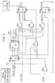
- FIG. 2 is a schematic diagram of an FM/Flash modulator in accordance with the invention.
- FIG. 3 is a schematic diagram of an FM/Flash demodulator in accordance with the invention.
- the Biphase or FM with Flash (FM/Flash) MODEM of the invention may be implemented in a standard cell ASIC along with a synchronous communication controller that has a built-in FM encoder/decoder.
- the synchronous communication controller may also have a digital phase lock loop built-in, so that one need not be incorporated into the MODEM.
- a 16 times oversampling clock is preferred in this implementation which provides for 16 counts per bit cell.
- Figure 1 illustrates the forms of signals modulated in accordance with different prior art encoding techniques as well as the reduced pulse width modulated signals of the invention.
- the uppermost signal form shown is the serial digital input to be encoded, followed by the prior art Non-Return-to-Zero (NRZ) coding format, and two corresponding forms for the FM1 and FM0 versions of Biphase encoding.
- the lower two signals are indicative of the corresponding forms produced by FM1/Flash and FM0/Flash encoding in accordance with the present invention.
- NRZ Non-Return-to-Zero
- the components of the FM/Flash MODEM are shown in Figures 2 and 3.
- the modulator as seen in Figure 2, is implemented using a 4-bit counter 30 that can be triggered to count once from zero up to fifteen when a START input is activated by the output of delay-flipflop 31. When the counter 30 wraps back to zero, it stops counting unless the START input is active at that time.
- the START input to the counter 30 is a synchronous FM encoded input and the CLR/ input is an asynchronous clear_not input through inverter (NOT) and NOR gate NOR2.
- Output QA of counter 30 is the least significant count output bit and QD is the most significant count output bit.
- the modulator is initialized to a known valid state as the RESET signal, input to NOR gates NOR2, is active.
- an FM encoded transmitted data signal from the Serial Controller, goes HIGH on the FM_TX input line
- the output of delay-flipflop 31 gets set to 1 causing the counter 30 to start counting at the next rising edge of the signal from the 16 times oversampling clock on 16X_CLK.
- counter 30 counts to 1
- the J input of J-K flip-flop 32 is set, and the output of the modulator, on line IR_TX, gets set at the rising edge of the signal on 16X_CLK starting an output pulse at HIGH level.
- the K input of J-K flip-flop 32 is set, which causes the output on IR_TX to be reset ending the pulse.
- This four count setting and resetting results in the sending of about 1/4 bit cell long pulse on line IR_TX to an IR source.
- the IR source converts the electronic pulse to a corresponding IR light pulse for transmission as part of an encoded signal to a demodulator.
- the IR_TX line gets cleared by an asynchronous clear signal regardless of the count of counter 30.
- This clear signal is provided to the CLRN port of D-flipflop 32 and the CLR/ input of counter 30 through the inverter (NOT) and NOR gate (NOR2). If the Biphase encoded signal on FM_TX happens to be a bit-cell long, the second 1/4 bit-cell long pulse will be sent on IR_TX at the count of 9, using the components as described in the preceding paragraph, and IR_TX gets reset at the count of 13.
- the first D-flipflop 31 that got set as the FM_TX signal made the transition from LOW to HIGH will be reset at the count of 3 and 11, by the output of D-flip-flop 33 so that the D-flip-flop 31 is ready to detect the next rising edge of the signal on FM_TX.
- the counter 30 gets cleared to zero either when it wraps back from count 15 or when the FM_TX input becomes LOW.
- the demodulator as shown in Figure 3 first detects a rising edge on the incoming infrared pulse signal, IR_RX, from an IR receiver that detects the IR 1/4 bit cell width light pulses output by the modulator's IR Source.
- IR_RX incoming infrared pulse signal
- latch 23 gets set, and a 5-bit counter 20 begins to count up starting from zero.
- the counter 20 is clocked at the rising edge of the 16X_CLK input.
- latch 21, between latches 25 and 26 gets set on the next rising edge of the clock pulse.
- the incoming IR_RX signal is fed directly to D-flipflop 24, and is sampled when latch 24 gets triggered by the output of latch 21, whereupon a half bit cell long demodulated FM encoded signal, FM_RX, is generated if IR_RX is HIGH.
- the FM_RX signal output from latch 24 is fed to a serial controller for the decoding of the FM encoding to NRZ format in an infrared communication system.
- D-flipflop 24 samples IR_RX at counts 3 and 11, and is cleared at the count of 19 upon detection by latch 25.
- the FM encoded FM_RX output signal is sampled by latch 22 at counts 4 and 12 and if FM_RX is LOW at that time, the D-flipflop 23 that detects a rising edge of IR_RX gets cleared so that it is ready to detect the next rising edge. At the count of 20, which is detected by latch 26, D-flipflop 23 will also get cleared regardless of the level of the FM_RX signal that was sampled prior to this. When the D-flipflop 23 gets cleared, the counter 20 also resets the count to zero and stays at that count until the next incoming rising edge is detected by D-flipflop 23.
- the demodulator includes logic to validate an incoming pulse.
- latch 21 gets set on the next rising edge of the clock pulse and the incoming IR_RX signal, fed directly to D-flipflop 24, is sampled when latch 24 gets triggered by the output of latch 21.
- the output FM_RX signal from latch 24 will go HIGH or LOW in accordance with the level of the sampled IR_RX signal.
- this FM_RX output signal is sampled by latch 22 at counts 4 and 12 and if FM_RX is LOW at those times, the D-flipflop 23 that detects a rising edge of IR_RX gets cleared so that it is ready to detect the next rising edge.
- the pulse level will be sampled after a predefined time, preferably 3 clock counts, which will be less than the width of a 1/4 bit cell pulse. If the sample is of a HIGH level, it is assumed the incoming pulse is valid and a HIGH level is output. If the sample is of a LOW level, the pulse is ignored and the system is reset to await the next one.
- This demodulator therefore puts out FM encoded data on line FM_RX from the incoming FM with Flash modulated signal on IR_RX. Consequently, the FM/Flash MODEM of the invention accepts FM encoded data as input and outputs FM encoded data after transmission between its components, so that any associated equipment or systems with which it is used need not be specially adapted to deal with its internal encoding, i.e., FM with Flash encoding.
- the Biphase or FM with FLASH MODEM of the invention can be used with both FM0 or FM1 encoded data as well as Manchester coded data and is suitable for synchronous communication.
- a full digital phase lock loop is not required but can be included as part of the demodulator, if desired, its implementation being within the purview of those of skill in the art.
- the FM with Flash MODEM described herein is particularly suitable for use in the Interoperable Multiprotocol Directed Infrared Wireless Communication Controller disclosed in our co-pending U.S. patent application Ser.No.(YO994-177) filed concurrently herewith and incorporated herein by reference.
- This MODEM also can be used in any communication controller that uses Biphase or FM modulation providing that the analog circuit that is used to amplify and filter the signal in the receiver can pass this modulated signal.
Landscapes
- Engineering & Computer Science (AREA)
- Computer Networks & Wireless Communication (AREA)
- Signal Processing (AREA)
- Physics & Mathematics (AREA)
- Spectroscopy & Molecular Physics (AREA)
- Electromagnetism (AREA)
- Optical Communication System (AREA)
- Dc Digital Transmission (AREA)
- Synchronisation In Digital Transmission Systems (AREA)
- Digital Transmission Methods That Use Modulated Carrier Waves (AREA)
Applications Claiming Priority (2)
| Application Number | Priority Date | Filing Date | Title |
|---|---|---|---|
| US323332 | 1994-10-14 | ||
| US08/323,332 US5610947A (en) | 1994-10-14 | 1994-10-14 | IR FM modem with flash modulation |
Publications (3)
| Publication Number | Publication Date |
|---|---|
| EP0707391A2 true EP0707391A2 (de) | 1996-04-17 |
| EP0707391A3 EP0707391A3 (de) | 1998-05-20 |
| EP0707391B1 EP0707391B1 (de) | 2004-04-07 |
Family
ID=23258757
Family Applications (1)
| Application Number | Title | Priority Date | Filing Date |
|---|---|---|---|
| EP95113154A Expired - Lifetime EP0707391B1 (de) | 1994-10-14 | 1995-08-22 | Flash-FM-Infrarotmodem |
Country Status (6)
| Country | Link |
|---|---|
| US (1) | US5610947A (de) |
| EP (1) | EP0707391B1 (de) |
| JP (1) | JP3065919B2 (de) |
| KR (1) | KR0163236B1 (de) |
| CN (1) | CN1095245C (de) |
| DE (1) | DE69532846T2 (de) |
Cited By (5)
| Publication number | Priority date | Publication date | Assignee | Title |
|---|---|---|---|---|
| WO1997042740A1 (fr) * | 1996-05-02 | 1997-11-13 | Gay Freres Vente Et Exportation S.A. | Systeme de transmission de signaux lumineux a faible consommation et dispositif memoire utilisant ce systeme |
| DE19653582A1 (de) * | 1996-12-20 | 1998-06-25 | Nokia Deutschland Gmbh | Einrichtung zum kabellosen optischen Übertragen von Video- und/oder Audioinformationen |
| FR2768881A1 (fr) * | 1997-09-24 | 1999-03-26 | St Microelectronics Sa | Dispositif de commande de l'echantillonnage d'un signal vehiculant des informations binaires codees selon un codage bi-phase |
| EP0943920A2 (de) * | 1998-03-16 | 1999-09-22 | Micronas Intermetall GmbH | Sensoreinrichtung und Verfahren zur Datenübertragung mit einer solchen Sensoreinrichtung |
| TWI489793B (zh) * | 2013-06-26 | 2015-06-21 | Univ Yuan Ze | FM0 encoding and Manchester encoding common encoders |
Families Citing this family (8)
| Publication number | Priority date | Publication date | Assignee | Title |
|---|---|---|---|---|
| TW256900B (de) * | 1993-11-25 | 1995-09-11 | Alps Electric Co Ltd | |
| JP3080907B2 (ja) * | 1997-07-22 | 2000-08-28 | 日本電気アイシーマイコンシステム株式会社 | 変復調方法および変復調装置 |
| JP3687947B2 (ja) * | 1999-03-17 | 2005-08-24 | シャープ株式会社 | 赤外線通信装置および通信方法、並びに情報機器装置 |
| WO2001017298A1 (en) * | 1999-09-02 | 2001-03-08 | Automated Business Companies | Communication and proximity authorization systems |
| US8639127B2 (en) * | 2002-03-06 | 2014-01-28 | Alcatel Lucent | Method and apparatus for improved jitter tolerance |
| WO2003077185A1 (en) | 2002-03-13 | 2003-09-18 | Koninklijke Philips Electronics N.V. | Communication station for communication with transponders and further communication stations with the aid of different protocols |
| KR100651883B1 (ko) * | 2005-08-29 | 2006-12-01 | 엘지전자 주식회사 | Fm-tx 기능을 구비한 영상기기 및 그 제어방법 |
| CN112491425B (zh) * | 2020-12-08 | 2024-02-27 | 中科计算技术创新研究院 | 灵活可配的射频硬件解码器 |
Family Cites Families (20)
| Publication number | Priority date | Publication date | Assignee | Title |
|---|---|---|---|---|
| US3665103A (en) * | 1969-12-16 | 1972-05-23 | Ibm | Synchronous frequency shift data transmission system in which opposite binary characterizations are transmitted as half cycles of a first carrier signal and as full cycles of a second carrier signal |
| US3683277A (en) * | 1970-04-13 | 1972-08-08 | Astrocon Corp | Communication system for binary coded data |
| US3743775A (en) * | 1972-01-12 | 1973-07-03 | Collins Radio Co | Data demodulator apparatus |
| US3890581A (en) * | 1972-12-27 | 1975-06-17 | Rixon | Digital FM (FSK) modulator |
| JPS5466111A (en) * | 1977-11-05 | 1979-05-28 | Sony Corp | Time code write system |
| US4377006A (en) * | 1979-07-12 | 1983-03-15 | Zenith Radio Corporation | IR Remote control system |
| WO1981001491A1 (fr) * | 1979-11-22 | 1981-05-28 | Siemens Ag | Station telephonique d'abonne |
| US4441193A (en) * | 1982-05-03 | 1984-04-03 | Burroughs Corporation | Frequency-encoding circuit for reducing distortion |
| DE3640003C2 (de) * | 1986-11-22 | 1996-07-25 | Schunk Produktionsgesellschaft | Verfahren und Vorrichtung zur Informationsübertragung, insbesondere für mobile Informationsträgersysteme |
| JPS6468162A (en) * | 1987-09-09 | 1989-03-14 | Man Design Co | Fsk demodulator |
| US4888791A (en) * | 1988-01-25 | 1989-12-19 | Barndt Sr Robert A | Clock decoder and data bit transition detector for fiber optic work station |
| US5128792A (en) * | 1989-11-06 | 1992-07-07 | Inncom International, Inc. | Self-synchronizing infra-red communication system |
| JPH0636509B2 (ja) * | 1990-06-22 | 1994-05-11 | 日本航空電子工業株式会社 | 光バス伝送方式 |
| JP2663746B2 (ja) * | 1991-05-30 | 1997-10-15 | 日本電気株式会社 | ディジタルfm変調装置 |
| US5214526A (en) * | 1991-06-04 | 1993-05-25 | Apple Computer, Inc. | Pulse modulated infrared data communications link |
| US5351249A (en) * | 1991-07-19 | 1994-09-27 | Interdigital Technology Corporation | Trellis coded FM digital communications system and method |
| JP3087459B2 (ja) * | 1991-09-27 | 2000-09-11 | 松下電器産業株式会社 | Fskデータ復調器 |
| US5297181A (en) * | 1992-01-17 | 1994-03-22 | Alesis | Method and apparatus for providing a digital audio interface protocol |
| US5289141A (en) * | 1992-10-13 | 1994-02-22 | Motorola, Inc. | Method and apparatus for digital modulation using concurrent pulse addition and subtraction |
| US5436590A (en) * | 1994-08-25 | 1995-07-25 | Northern Telecom Limited | Digital FSK demodulator with automatic offset cancellation |
-
1994
- 1994-10-14 US US08/323,332 patent/US5610947A/en not_active Expired - Fee Related
-
1995
- 1995-05-09 CN CN95105473A patent/CN1095245C/zh not_active Expired - Fee Related
- 1995-08-22 DE DE69532846T patent/DE69532846T2/de not_active Expired - Lifetime
- 1995-08-22 EP EP95113154A patent/EP0707391B1/de not_active Expired - Lifetime
- 1995-10-11 KR KR1019950034826A patent/KR0163236B1/ko not_active Expired - Fee Related
- 1995-10-12 JP JP7264497A patent/JP3065919B2/ja not_active Expired - Fee Related
Cited By (9)
| Publication number | Priority date | Publication date | Assignee | Title |
|---|---|---|---|---|
| WO1997042740A1 (fr) * | 1996-05-02 | 1997-11-13 | Gay Freres Vente Et Exportation S.A. | Systeme de transmission de signaux lumineux a faible consommation et dispositif memoire utilisant ce systeme |
| DE19653582A1 (de) * | 1996-12-20 | 1998-06-25 | Nokia Deutschland Gmbh | Einrichtung zum kabellosen optischen Übertragen von Video- und/oder Audioinformationen |
| US6208445B1 (en) | 1996-12-20 | 2001-03-27 | Nokia Gmbh | Apparatus for wireless optical transmission of video and/or audio information |
| EP0849895A3 (de) * | 1996-12-20 | 2001-05-30 | NOKIA TECHNOLOGY GmbH | Einrichtung zum kabellosen optischen Übertragen von Video-und/oder Audioinformationen |
| FR2768881A1 (fr) * | 1997-09-24 | 1999-03-26 | St Microelectronics Sa | Dispositif de commande de l'echantillonnage d'un signal vehiculant des informations binaires codees selon un codage bi-phase |
| EP0905946A1 (de) * | 1997-09-24 | 1999-03-31 | STMicroelectronics SA | Reglung der Abtastung von Biphasensignale |
| US6097322A (en) * | 1997-09-24 | 2000-08-01 | Stmicroelectronics S.A. | Device and method for controlling the sampling of a signal conveying binary information coded according to a two-phase code |
| EP0943920A2 (de) * | 1998-03-16 | 1999-09-22 | Micronas Intermetall GmbH | Sensoreinrichtung und Verfahren zur Datenübertragung mit einer solchen Sensoreinrichtung |
| TWI489793B (zh) * | 2013-06-26 | 2015-06-21 | Univ Yuan Ze | FM0 encoding and Manchester encoding common encoders |
Also Published As
| Publication number | Publication date |
|---|---|
| KR960016301A (ko) | 1996-05-22 |
| DE69532846T2 (de) | 2005-05-19 |
| JPH08204759A (ja) | 1996-08-09 |
| US5610947A (en) | 1997-03-11 |
| CN1095245C (zh) | 2002-11-27 |
| KR0163236B1 (ko) | 1998-12-01 |
| CN1134066A (zh) | 1996-10-23 |
| EP0707391B1 (de) | 2004-04-07 |
| EP0707391A3 (de) | 1998-05-20 |
| DE69532846D1 (de) | 2004-05-13 |
| JP3065919B2 (ja) | 2000-07-17 |
Similar Documents
| Publication | Publication Date | Title |
|---|---|---|
| US5610947A (en) | IR FM modem with flash modulation | |
| US5461379A (en) | Digital coding technique which avoids loss of synchronization | |
| US7352771B2 (en) | Data collision detection device and method | |
| US4852122A (en) | Modem suited for wireless communication channel use | |
| US6437710B1 (en) | Encoder within a communication system that avoids encoded DC accumulation and can use coding violations to synchronize a decoder and detect transmission errors | |
| EP2108225B2 (de) | Kommunikationsverfahren und einrichtung | |
| US5602873A (en) | Flash NRZI infrared modem | |
| EP1453239A1 (de) | Packetformat mit zwei verschiedenen Leitungscodes und geeigneter Empfänger | |
| US4887269A (en) | Apparatus for the reception of radio broadcasted digital signals | |
| JP3267445B2 (ja) | エラー検出回路および方法 | |
| US7469023B2 (en) | Manchester code delta detector | |
| RU97107459A (ru) | Способ и устройство для модуляции цифровых данных, в частности, проблесковый инфракрасный модем с кодированием типа nrzi | |
| WO2021074558A1 (en) | Adaptive coding for wireless communication | |
| JP2000134269A5 (de) | ||
| US6839006B1 (en) | Communication device | |
| US20030058501A1 (en) | Wireless communication system comprising a host and a guest, and method associated herewith | |
| JPS6222293B2 (de) | ||
| JPH0946378A (ja) | シリアル・データ伝送装置の転送データ変調/復調方式 | |
| JPH03109842A (ja) | Oa機器間の信号伝送方法 | |
| US20020136313A1 (en) | Time-sectionalized demodulator | |
| JP2751271B2 (ja) | ディジタル送受信装置 | |
| CN119788097A (zh) | Rzi编码转nrz编码的转换方法及解码电路、芯片 | |
| JPS62142435A (ja) | デ−タ伝送方式 |
Legal Events
| Date | Code | Title | Description |
|---|---|---|---|
| PUAI | Public reference made under article 153(3) epc to a published international application that has entered the european phase |
Free format text: ORIGINAL CODE: 0009012 |
|
| AK | Designated contracting states |
Kind code of ref document: A2 Designated state(s): DE FR GB |
|
| K1C1 | Correction of patent application (title page) published |
Effective date: 19960417 |
|
| 17P | Request for examination filed |
Effective date: 19960827 |
|
| PUAL | Search report despatched |
Free format text: ORIGINAL CODE: 0009013 |
|
| AK | Designated contracting states |
Kind code of ref document: A3 Designated state(s): DE FR GB |
|
| 17Q | First examination report despatched |
Effective date: 20030512 |
|
| GRAP | Despatch of communication of intention to grant a patent |
Free format text: ORIGINAL CODE: EPIDOSNIGR1 |
|
| RAP1 | Party data changed (applicant data changed or rights of an application transferred) |
Owner name: INTERNATIONAL BUSINESS MACHINES CORPORATION |
|
| GRAS | Grant fee paid |
Free format text: ORIGINAL CODE: EPIDOSNIGR3 |
|
| GRAA | (expected) grant |
Free format text: ORIGINAL CODE: 0009210 |
|
| AK | Designated contracting states |
Kind code of ref document: B1 Designated state(s): DE FR GB |
|
| REG | Reference to a national code |
Ref country code: GB Ref legal event code: FG4D |
|
| REF | Corresponds to: |
Ref document number: 69532846 Country of ref document: DE Date of ref document: 20040513 Kind code of ref document: P |
|
| ET | Fr: translation filed | ||
| PLBE | No opposition filed within time limit |
Free format text: ORIGINAL CODE: 0009261 |
|
| STAA | Information on the status of an ep patent application or granted ep patent |
Free format text: STATUS: NO OPPOSITION FILED WITHIN TIME LIMIT |
|
| 26N | No opposition filed |
Effective date: 20050110 |
|
| REG | Reference to a national code |
Ref country code: GB Ref legal event code: 746 Effective date: 20090714 |
|
| PGFP | Annual fee paid to national office [announced via postgrant information from national office to epo] |
Ref country code: FR Payment date: 20100818 Year of fee payment: 16 Ref country code: DE Payment date: 20100826 Year of fee payment: 16 |
|
| PGFP | Annual fee paid to national office [announced via postgrant information from national office to epo] |
Ref country code: GB Payment date: 20100819 Year of fee payment: 16 |
|
| GBPC | Gb: european patent ceased through non-payment of renewal fee |
Effective date: 20110822 |
|
| REG | Reference to a national code |
Ref country code: FR Ref legal event code: ST Effective date: 20120430 |
|
| REG | Reference to a national code |
Ref country code: DE Ref legal event code: R119 Ref document number: 69532846 Country of ref document: DE Effective date: 20120301 |
|
| PG25 | Lapsed in a contracting state [announced via postgrant information from national office to epo] |
Ref country code: FR Free format text: LAPSE BECAUSE OF NON-PAYMENT OF DUE FEES Effective date: 20110831 Ref country code: GB Free format text: LAPSE BECAUSE OF NON-PAYMENT OF DUE FEES Effective date: 20110822 |
|
| PG25 | Lapsed in a contracting state [announced via postgrant information from national office to epo] |
Ref country code: DE Free format text: LAPSE BECAUSE OF NON-PAYMENT OF DUE FEES Effective date: 20120301 |