EP0707766B1 - Recepteur depart-arret - Google Patents
Recepteur depart-arret Download PDFInfo
- Publication number
- EP0707766B1 EP0707766B1 EP94920350A EP94920350A EP0707766B1 EP 0707766 B1 EP0707766 B1 EP 0707766B1 EP 94920350 A EP94920350 A EP 94920350A EP 94920350 A EP94920350 A EP 94920350A EP 0707766 B1 EP0707766 B1 EP 0707766B1
- Authority
- EP
- European Patent Office
- Prior art keywords
- data
- bit
- signal
- bits
- word
- Prior art date
- Legal status (The legal status is an assumption and is not a legal conclusion. Google has not performed a legal analysis and makes no representation as to the accuracy of the status listed.)
- Expired - Lifetime
Links
Images


Classifications
-
- H—ELECTRICITY
- H04—ELECTRIC COMMUNICATION TECHNIQUE
- H04L—TRANSMISSION OF DIGITAL INFORMATION, e.g. TELEGRAPHIC COMMUNICATION
- H04L25/00—Baseband systems
- H04L25/38—Synchronous or start-stop systems, e.g. for Baudot code
- H04L25/40—Transmitting circuits; Receiving circuits
Definitions
- This invention relates to a method of extracting data words from a binary serial bit stream, for example a bit stream representing call identity information.
- CLASSTM signaling in which the call identity information is transmitted as a CPBFSK (continuous phase binary frequency shift keying) signal between the ringing tones of a calling signal.
- CPBFSK continuous phase binary frequency shift keying
- the CPBFSK signal can typically contain information for services such as calling number delivery (CND), calling identity delivery on call waiting (CIDCW), and calling name delivery (CNAM).
- CND calling number delivery
- CIDCW calling identity delivery on call waiting
- CNAM calling name delivery
- the information contained in the CLASSTM signal is currently extracted by circuitry incorporated in the user equipment or an add-on unit and presented to the user on an LCD display.
- the CPBFSK signal can contain a wealth of information, and in the future it is likely that increasing amounts of information will become available. It is important to be able to extract this information as useful data words, either simply for display on the local display device or for interfacing with a computer. For example, a telemarketing firm might wish to extract the number of the call party and match it with information in its local database so as to bring up information about the customer prior to accepting an incoming call.
- the CPBFSK signal is first demodulated by a CPBFSK demodulator (e.g. Motorola MC145447).
- the demodulator output is a serial binary data bit stream.
- the 8-bit data words in the bit stream must be extracted before the information can be further processed by a microprocessor for example.
- UART universal asynchronous receiver transmitter
- the UART may be a discrete unit (e.g. National Semiconductor NS16450), or embedded in a microprocessor (e.g. Intel 8051).
- the bit stream goes into the serial input of the UART which extracts the 8-bit words and presents them at an 8-bit wide parallel output.
- An object of the invention is to provide a simplified device capable of decoding CLASSTM signaling that has a low power consumption.
- the invention provides a method of extracting data words from a binary serial bit stream having a fixed bit rate and consisting of fixed length words of n bits each, where n is an integer, each word being preceded by a start bit and followed by one or more stop bits, comprising detecting a predetermined identifiable transition in said bit stream preceding each data word, outputting said bit stream as a data signal (DATA), generating a clock signal (DCLK) consisting of n clock pulses in response to each detection of said predetermined transition in coincidence with the bits the data word following said predetermined transition, generating a data ready signal (DR) after the passage of n bits to delineate the word boundary, and extracting said data words from said bit stream using said thus generated clock pulses and said data ready signal.
- DATA data signal
- DCLK clock signal
- DR data ready signal
- An important aspect of the invention is the extraction of fixed bit length data words from a binary serial bit stream without a discrete UART device, nor the high hardware overhead associated with a full feature UART device included into an integrated circuit performing other functions, nor the need for the UART function to be implemented in microprocessor software.
- the invention also provides a circuit for facilitating the extraction of data words from a binary serial bit stream having a fixed bit rate and consisting of fixed length words of n bits each, where n is an integer, each word being preceded by a start bit and followed by one or more stop bits, comprising means for detecting a predetermined identifiable transition in said bit stream preceding each data word, means for outputting said bit stream as a data signal (DATA), means for generating a clock signal (DCLK) consisting of n clock pulses in response to each detection of said predetermined transition in coincidence with the bits the data word following said predetermined transition, and means for generating a data ready signal (DR) after the passage of n bits to delineate the word boundary, whereby said data words can be extracted from said bit stream with the aid of said thus generated clock pulses and said data ready signal.
- DATA data signal
- DCLK clock signal
- DR data ready signal
- the circuit in effect provides a three-wire interface that can be implemented on a single chip complete with a CPBFSK demodulator.
- the three-wire interface provides a data signal, which is a serial bit stream, a DCLK (data clock) signal which identifies the ideal sample instance of the data bits and the data words of the serial bit stream, and a DR (data ready signal) which signifies the end of a data word.
- the circuit is suitable, for example, for the word format specified by R-35, R-42 (transmission rate), R-44, and R-46 of Bellcore document TR-TSY-00003, "Voiceband Data Transmission Interface Generic Requirements".
- Any suitable fixed bit rate can be implemented, but commonly a bit rate of 1200 bps and 8-bit word length are employed.
- the circuit when implemented as a single chip receives the incoming analog CPBFSK signal from the telephone line.
- the demodulator produces the data stream, which is output as the data signal and the DCLK and DR signals are output as part of the three-wire interface.
- These can be fed to a shift register to generate parallel data words, or alternatively the data and data clock signals are fed to an input port of a microprocessor with the data ready signal being supplied through an interrupt request line.
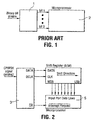
- Figure 1 shows a prior art data extraction circuit.
- the binary bit stream from a separate CPBFSK demodulator (not shown) is inputted to a UART (universal asynchronous receiver transmitter) 1 that outputs a parallel stream of binary words for application to the bus of microprocessor 2.
- the UART which may be for example a national semiconductor NS16450 chip, is a relatively complex device that is programmed according to the characteristics of the data stream. Alternatively the UART can be embedded in the microprocessor itself.
- FIG. 2 shows a circuit in accordance with the invention.
- An analog CPBFSK signal direct from a telephone line is input to CNIC chip 3, which incorporates a CPBFSK demodulator.
- the CNIC chip 3, which will be described in more detail with reference to Figure 7, outputs a serial bit stream as a data signal for application to the data input of shift register 4.
- CNIC chip 3 generates a data clock signal DCLK for application to the clock input of shift register 4. On each clock pulse, the data is shifted one position along the 8-bit shift register 4.
- the CNIC chip 3 also generates a data ready signal (DR) for input to an interrupt request line of a microprocessor 5 which receives at a parallel input port parallel data from the shift register 4. Upon receipt of each DR signal, contents of the shift register are transferred in parallel to the input of microprocessor 5.
- DR data ready signal
- Figure 3 shows an alternative embodiment where the three-wire output of the CNIC chip 3 is applied directly to a microprocessor 5.
- the DCLK and DATA signals are connected to 2 bits of the microprocessor input port.
- the microprocessor software saves the DATA bit whenever it detects a logical 0 to 1 transition at the DCLK bit.
- An 8-bit word is then assembled from the last 8 saved bits when DR goes low.
- DR may be applied as an interrupt request of the microprocessor or a third bit of the input port.
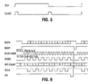
- Figure 4 shows the demodulated DATA signal 9 coming from the CPBFSK demodulator.
- This signal comprises two stop bits 7 and a start bit 8.
- Each byte (8-bit word) is preceded by a start bit and followed by at least one stop bit.
- the stop to start transition (DATA changes from 1 to 0) is used as an event trigger.
- a set of eight 50% duty cycle DCLK pulses are generated by the trigger, one for each data bit. No pulse is generated for the start and stop bits. Each clock cycle is nominally 1200 Hz to coincide with the data rate.
- the low to high transition of DCLK is used to read DATA at the nominal half way point of each data bit.
- DCLK is used to clock the 8 bit serial-in-parallel-out shift register receiving the DATA signal.
- a low pulse is generated at the open drain DR output after the last data bit to delineate the word boundary. This is used as to read the output of the serial-in-parallel-out shift register or as a microprocessor interrupt to group the preceding 8 data bits into a word.
- the serial bit stream (DATA) should be at logical 1 when no words are being received.
- the first logical 0 in the serial bit stream is taken to be a stop bit to start bit transition, hence the beginning of an 8-bit word.
- the first logical 0 in the serial bit stream must occur only at a received bit boundary.
- DATA is connected to the data input of an 8-bit shift register shifted by a high going clock (e.g. 74HC164), and DCLK to the shift register's clock input.
- the shift register outputs the 8-bit word every time DR is low.
- the protocol specifies an 8-bit data word bounded by a start bit (logical 0) and a stop bit (logical 1)
- the data bit and word timings can be extracted for the entire message at a specific baud rate once the beginning of the first word has been determined.
- the regenerated bit rate does not have to match that of the transmitter exactly because the bit timing is re-aligned at the beginning of every word.
- the timing extractor works by synchronizing to the stop to start bit transition at the beginning of the word. It is then a simple task to generate bit and word timings for a fixed baud rate.
- the circuit in Figure 7 works for one start bit only. Any number of stop bits is acceptable because only the stop to start bit transition is required.
- the data may be preceded by either one of two preambles: a 300 bits repeating 1010 channel seizure signal followed by an 80+/-10 bit mark interval for on-hook data transmission, or just the mark interval for off-hook data transmission.
- the recovered data words are (the bits are in the order they are received, start and stop bits have been stripped): 10101010 ... 10101010 and one of 10101010 101011 10101111 10111111 11111111 followed by the data words.
- the marks are invisible because no bit and word timing is generated. They are just stop bits.
- There are 5 possibilities for the last data word in the channel seizure signal because the conier detector may have become acdve in the middle of a word at the beginning of the preamble.
- the number of 10101010 words is less than 30 because the first words are not recognized: DATA is forced to 1 while the fsk signal is being integrated by the carrier detector.
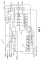
- RDATA is the hardlimited lowpass filter output. It is sampled at DCLK's rising edge. RDATA I to 0 transition is detected with 2 DFF's. If CDB is low when the transition occurs, the JKFF will be set. ARM goes high at the next DCLK rising edge. If ARM is high, the second DFF's output becomes QDATA, the interlock output. When CDB is deactivated, ARM is cleared asynchronous to the bit cell boundary because all valid data had already been received.
- a clock signal DCLK is generated by dividing a local oscillator frequency by 48. This is then divided by 62 to arrive at the clock rate DCLK for the circuit 4.
- the rising edge of DCLK normally occurs at the middle of a bit cell, which is the ideal sample instant.
- DR is low during the first half of the stop bit, and this denotes the end of the word.
- QDATA is the raw binary serial bit stream. QDATA change is synchronous with the rising edge of CLK. It is delayed by half a CLK cycle to become DATA.
- the qualified data QDATA is monitored by two D type flip flops 10,11 ( Figure 7). While timing extraction is not in progress, the (J-K type flip flop) output BUSY is low to keep the timing extractor under reset. On the QDATA 1 to 0 transition, BUSY is set. It remains set until after the bit and word timings for 1 word have been generated. The next QDATA 1 to 0 transition thereafter restarts the extractor.
- the main elements of the timing extractor are a bit time counter 12 and a bit counter 13.
- the bit time counter 12 divides CLK by 62 to generate one bit time. It is advanced by CLK's falling edge. First, a half bit time counter divides CLK by 31. Then the MSB's falling edge clocks a toggle flip-flop so that the output DIV62 has a 50% duty cycle. The half bit time count is from 1 to 31. The count is evaluated by the falling edge of CLKX2 whose rate is twice that of CLK (see Figure 5). When the count cycles from 31 to 0, a half CLK long pulse DIV31RSTB is generated to preset the count to 1.
- the bit count and DIV62 are evaluated to obtain the bit and word timings DCLK, DR shown in Figure 6.
- the count sequence is F-0-...-7-8-9-F.
- DCLK is low when the count is from 0 to 7 and DIV62 is low.
- DR is low when the count is 8 and DIV 62 is low.
- BUSY goes low and puts the timing extractor back into idle.
- FIG. 8 shows a more detailed timing diagram, in which DIV31st is the output of a D type flip-flop clocked by DCLKX2.
- the incoming analog signal is first passed to a CPBFSK demodulator, which implements a conventional scheme (see for example Carlos A. Laber and Pierre P. Lemaitre, "A monolithic 1200 baud FSK CMOS modem", IEEE Journal of Solid-State Circuits, vol. SC-19, pp. 861-869, December 1984).
- the demodulator consists of an anti-aliasing filter, band pass filter, sign bit delay, and multiplier and low pass filter.
- the demodulator output is the low pass filter output RDATA shown as an input to Figure 7.
- the described arrangement thus provides a convenient way of extracting information embedded in a CLASSTM or similar signal. It can be used as a source of data for call display devices or as an input to more sophisticated computer-based systems, which for example look up in a database data relating to a calling party and display it before the called party even answers the telephone.
Landscapes
- Engineering & Computer Science (AREA)
- Computer Networks & Wireless Communication (AREA)
- Signal Processing (AREA)
- Digital Transmission Methods That Use Modulated Carrier Waves (AREA)
- Dc Digital Transmission (AREA)
- Synchronisation In Digital Transmission Systems (AREA)
Abstract
Claims (11)
- Méthode d'extraction de mots de données d'un train binaire de bits série ayant un débit binaire fixe et constitué de mots de longueur fixe de n bits chacun, n étant un nombre entier, chaque mot étant précédé d'un bit de départ et suivi d'un ou de plusieurs bits d'arrêt, caractérisée en ce qu'elle comprend la détection dans ledit train binaire d'une transition prédéterminée identifiable précédant chaque mot de données, la sortie dudit train binaire en tant que signal de données (DATA), l'émission d'un signal d'horloge (DCLK) constitué par n impulsions d'horloge en réponse à chaque détection de ladite transition prédéterminée et en coïncidence avec les bits du mot de données suivant ladite transition prédéterminée, l'émission d'un signal de données prêtes (DR) après le passage de n bits afin de marquer la limite du mot, et l'extraction desdits mots de données dudit train binaire à l'aide desdites impulsions d'horloge ainsi émises et dudit signal de données prêtes.
- Méthode selon la revendication 1, caractérisée en ce que ledit signal de données est envoyé en tant qu'entrée sur un registre à décalage qui est décalé par ledit signal d'horloge, et en ce que des mots de données parallèles sont sortis dudit registre à décalage à la réception dudit signal de données prêtes.
- Méthode selon la revendication 1, caractérisée en ce que ledit signal de données et ledit signal d'horloge sont envoyés sur deux bits d'un port d'entrée d'un microprocesseur, et en ce que ledit microprocesseur est programmé pour sauvegarder un bit de données à chaque fois qu'il détecte une transition logique pendant une impulsion d'horloge, et pour assembler un mot de données de n bits à partir des n derniers bits précédant la réception du signal de données prêtes.
- Méthode selon la revendication 1, caractérisée en ce que ledit signal de données prêtes est envoyé au microprocesseur en tant que demande d'interruption.
- Méthode selon la revendication 1, caractérisée en ce que ladite transition prédéterminée identifiable est un bit de transition d'arrêt / départ.
- Circuit destiné à faciliter l'extraction de mots de données d'un train binaire de bits série ayant un débit binaire fixe et constitué de mots de longueur fixe de n bits chacun, n étant un nombre entier, chaque mot étant précédé d'un bit de départ et suivi d'un ou de plusieurs bits d'arrêt, caractérisé en ce qu'il comprend un moyen permettant la détection dans ledit train binaire d'une transition prédéterminée identifiable précédant chaque mot de données, un moyen permettant la sortie dudit train binaire en tant que signal de données (DATA), un moyen permettant l'émission d'un signal d'horloge (DCLK) constitué par n impulsions d'horloge en réponse à chaque détection de ladite transition prédéterminée et en coïncidence avec les bits du mot de données suivant ladite transition prédéterminée, et un moyen permettant l'émission d'un signal de données prêtes (DR) après le passage de n bits afin de marquer la limite du mot, lesdits mots de données pouvant être extraits dudit train binaire à l'aide desdites impulsions d'horloge ainsi émises et dudit signal de données prêtes.
- Circuit selon la revendication 6, comprenant en outre un registre à décalage qui est décalé par ledit signal d'horloge, et qui génère en sortie des mots de données parallèles à la réception dudit signal de données prêtes.
- Circuit selon la revendication 6, comprenant en outre un microprocesseur, ledit signal d'horloge et ledit signal de données étant envoyés sur deux bits d'un port d'entrée de celui-ci, ledit microprocesseur étant programmé pour sauvegarder un bit de données à chaque fois qu'il détecte une transition logique pendant une impulsion d'horloge, et pour assembler un mot de données de n bits à partir des n derniers bits précédant la réception du signal de données prêtes.
- Circuit selon la revendication 6, caractérisé en ce que ledit signal de données prêtes est envoyé au microprocesseur en tant que demande d'interruption.
- Circuit selon la revendication 6, comprenant en outre un démodulateur pour générer ledit train binaire à partir d'un signal analogique.
- Circuit selon la revendication 6, caractérisé en outre en ce que ledit démodulateur est un démodulateur de type CPBFSK (Channel Program Block Frequency Shift Keying = modulation par déplacement de fréquence de bloc de programme de canal) monté dans un circuit intégré unique comportant un moyen permettant la détection dans ledit train binaire d'une transition prédéterminée identifiable précédant chaque mot de données, ledit moyen permettant la sortie dudit train binaire en tant que signal de données (DATA), et ledit moyen permettant l'émission d'un signal d'horloge.
Applications Claiming Priority (3)
| Application Number | Priority Date | Filing Date | Title |
|---|---|---|---|
| CA002099838A CA2099838C (fr) | 1993-07-05 | 1993-07-05 | Methode d'extraction de mots de donnees incorpores a une chaine binaire serie |
| CA2099838 | 1993-07-05 | ||
| PCT/CA1994/000363 WO1995002296A1 (fr) | 1993-07-05 | 1994-07-04 | Recepteur depart-arret |
Publications (2)
| Publication Number | Publication Date |
|---|---|
| EP0707766A1 EP0707766A1 (fr) | 1996-04-24 |
| EP0707766B1 true EP0707766B1 (fr) | 1997-06-04 |
Family
ID=4151894
Family Applications (1)
| Application Number | Title | Priority Date | Filing Date |
|---|---|---|---|
| EP94920350A Expired - Lifetime EP0707766B1 (fr) | 1993-07-05 | 1994-07-04 | Recepteur depart-arret |
Country Status (6)
| Country | Link |
|---|---|
| US (1) | US5917872A (fr) |
| EP (1) | EP0707766B1 (fr) |
| JP (1) | JPH09502578A (fr) |
| CA (1) | CA2099838C (fr) |
| DE (1) | DE69403659T2 (fr) |
| WO (1) | WO1995002296A1 (fr) |
Families Citing this family (7)
| Publication number | Priority date | Publication date | Assignee | Title |
|---|---|---|---|---|
| US5864754A (en) * | 1996-02-05 | 1999-01-26 | Hotto; Robert | System and method for radio signal reconstruction using signal processor |
| RU2134025C1 (ru) * | 1998-03-11 | 1999-07-27 | Закрытое акционерное общество "Информационные технологии и системы" | Устройство для приема и обработки информации |
| JP3666237B2 (ja) * | 1998-03-31 | 2005-06-29 | セイコーエプソン株式会社 | 情報処理装置及び電子機器 |
| US7110381B1 (en) * | 2001-03-19 | 2006-09-19 | Cisco Systems Wireless Networking (Australia) Pty Limited | Diversity transceiver for a wireless local area network |
| US20030048862A1 (en) * | 2001-09-10 | 2003-03-13 | Hsin-Hsien Lee | Automatic calibration & synchronization for digital asynchronous communication |
| US7460624B2 (en) * | 2004-03-18 | 2008-12-02 | Motorola, Inc. | Method and system of reducing collisions in an asynchronous communication system |
| US9367495B1 (en) * | 2008-09-30 | 2016-06-14 | Lattice Semiconductor Corporation | High speed integrated circuit interface |
Family Cites Families (8)
| Publication number | Priority date | Publication date | Assignee | Title |
|---|---|---|---|---|
| US3946379A (en) * | 1974-05-31 | 1976-03-23 | Rca Corporation | Serial to parallel converter for data transmission |
| US4447804A (en) * | 1981-06-22 | 1984-05-08 | The United States Of America As Represented By The Secretary Of The Navy | Serial to parallel data conversion interface circuit |
| US4768163A (en) * | 1984-05-07 | 1988-08-30 | Honeywell Bull Inc. | Magnetic stripe and wand reader interface employing off-the-shelf programmable communications interface |
| US4764896A (en) * | 1985-07-01 | 1988-08-16 | Honeywell Inc. | Microprocessor assisted memory to memory move apparatus |
| DE4015041A1 (de) * | 1990-05-10 | 1991-11-14 | Siemens Ag | Verfahren zur seriellen uebertragung von daten |
| US5313496A (en) * | 1990-12-26 | 1994-05-17 | Trw Inc. | Digital demodulator circuit |
| DE9214546U1 (de) * | 1992-07-02 | 1992-12-17 | Siemens AG, 8000 München | Schaltungsanordnung zur Überwachung des seriellen Datenaustauschs zwischen Datenverarbeitungsanlagen |
| US5394109A (en) * | 1994-02-17 | 1995-02-28 | Northern Telecom Limited | Digital FSK demodulator with offset cancellation |
-
1993
- 1993-07-05 CA CA002099838A patent/CA2099838C/fr not_active Expired - Fee Related
-
1994
- 1994-07-04 WO PCT/CA1994/000363 patent/WO1995002296A1/fr not_active Ceased
- 1994-07-04 JP JP7503726A patent/JPH09502578A/ja active Pending
- 1994-07-04 EP EP94920350A patent/EP0707766B1/fr not_active Expired - Lifetime
- 1994-07-04 US US08/583,064 patent/US5917872A/en not_active Expired - Lifetime
- 1994-07-04 DE DE69403659T patent/DE69403659T2/de not_active Expired - Fee Related
Also Published As
| Publication number | Publication date |
|---|---|
| DE69403659T2 (de) | 1998-01-08 |
| US5917872A (en) | 1999-06-29 |
| EP0707766A1 (fr) | 1996-04-24 |
| JPH09502578A (ja) | 1997-03-11 |
| CA2099838A1 (fr) | 1995-01-06 |
| DE69403659D1 (de) | 1997-07-10 |
| WO1995002296A1 (fr) | 1995-01-19 |
| CA2099838C (fr) | 2000-01-18 |
Similar Documents
| Publication | Publication Date | Title |
|---|---|---|
| US6385235B1 (en) | Direct digital access arrangement circuitry and method for connecting to phone lines | |
| US4029900A (en) | Digital synchronizing signal recovery circuits for a data receiver | |
| US20050036604A1 (en) | Direct digital access arrangement circuitry and method for connecting DSL circuitry to phone lines | |
| GB2118400A (en) | Switching digital data signals | |
| US6160857A (en) | Demodulator for frequency shift keying signals | |
| EP0707766B1 (fr) | Recepteur depart-arret | |
| US6408034B1 (en) | Framed delta sigma data with unlikely delta sigma data patterns | |
| US6178185B1 (en) | Network interface device, method and article of manufacture for providing high bit rate access over robbed bit | |
| CN1208923C (zh) | 卫星定位系统同步方法 | |
| US6272184B1 (en) | Non-coherent frequency shift keying detection scheme | |
| CA1128630A (fr) | Circuit de synchronisation de donnees | |
| US5579320A (en) | Channel unit transmission for removing false data bits in adjacent unterminated channel slots for D4 and SLC-96 channel banks | |
| WO2000062469A1 (fr) | Dispositif de synchronisation pour equipement connecte au reseau telephonique public | |
| JPH07240947A (ja) | 加入者系デジタル伝送装置 | |
| Horlacher et al. | Voiceband Four-Phase Data Set for Global Communication | |
| JP2891985B1 (ja) | 発呼者番号受信パッケージの試験方法 | |
| CA2100633A1 (fr) | Methode pour mettre a l'heure de facon automatique par ligne telephonique l'horloge d'un ordinateur personnel | |
| Berberi | Single-chip transceiver enables digital networks to meet global demands | |
| JPS62132450A (ja) | フレ−ムデ−タサンプリング同期獲得装置 | |
| WO1994011952A1 (fr) | Dispositif d'extraction de pseudo-signal d'horloge | |
| JPH0846722A (ja) | Isdn端末装置 | |
| JPS62266937A (ja) | Pcm信号の同期方法 | |
| KR20000050287A (ko) | 호출자 정보 표시 전화기의 호출자 정보 신호 디코딩 방법 | |
| JPH03184447A (ja) | モデム | |
| JPH0621935A (ja) | Isdn−sインタフェース回路 |
Legal Events
| Date | Code | Title | Description |
|---|---|---|---|
| PUAI | Public reference made under article 153(3) epc to a published international application that has entered the european phase |
Free format text: ORIGINAL CODE: 0009012 |
|
| 17P | Request for examination filed |
Effective date: 19960119 |
|
| AK | Designated contracting states |
Kind code of ref document: A1 Designated state(s): DE FR GB IT |
|
| GRAG | Despatch of communication of intention to grant |
Free format text: ORIGINAL CODE: EPIDOS AGRA |
|
| 17Q | First examination report despatched |
Effective date: 19960816 |
|
| GRAH | Despatch of communication of intention to grant a patent |
Free format text: ORIGINAL CODE: EPIDOS IGRA |
|
| GRAH | Despatch of communication of intention to grant a patent |
Free format text: ORIGINAL CODE: EPIDOS IGRA |
|
| GRAA | (expected) grant |
Free format text: ORIGINAL CODE: 0009210 |
|
| AK | Designated contracting states |
Kind code of ref document: B1 Designated state(s): DE FR GB IT |
|
| REF | Corresponds to: |
Ref document number: 69403659 Country of ref document: DE Date of ref document: 19970710 |
|
| ITF | It: translation for a ep patent filed | ||
| ET | Fr: translation filed | ||
| PLBE | No opposition filed within time limit |
Free format text: ORIGINAL CODE: 0009261 |
|
| 26N | No opposition filed | ||
| REG | Reference to a national code |
Ref country code: GB Ref legal event code: IF02 |
|
| PG25 | Lapsed in a contracting state [announced via postgrant information from national office to epo] |
Ref country code: IT Free format text: LAPSE BECAUSE OF NON-PAYMENT OF DUE FEES Effective date: 20050704 |
|
| PGFP | Annual fee paid to national office [announced via postgrant information from national office to epo] |
Ref country code: DE Payment date: 20070628 Year of fee payment: 14 |
|
| PGFP | Annual fee paid to national office [announced via postgrant information from national office to epo] |
Ref country code: GB Payment date: 20070704 Year of fee payment: 14 |
|
| PGFP | Annual fee paid to national office [announced via postgrant information from national office to epo] |
Ref country code: FR Payment date: 20070710 Year of fee payment: 14 |
|
| GBPC | Gb: european patent ceased through non-payment of renewal fee |
Effective date: 20080704 |
|
| PG25 | Lapsed in a contracting state [announced via postgrant information from national office to epo] |
Ref country code: DE Free format text: LAPSE BECAUSE OF NON-PAYMENT OF DUE FEES Effective date: 20090203 |
|
| REG | Reference to a national code |
Ref country code: FR Ref legal event code: ST Effective date: 20090331 |
|
| PG25 | Lapsed in a contracting state [announced via postgrant information from national office to epo] |
Ref country code: GB Free format text: LAPSE BECAUSE OF NON-PAYMENT OF DUE FEES Effective date: 20080704 |
|
| PG25 | Lapsed in a contracting state [announced via postgrant information from national office to epo] |
Ref country code: FR Free format text: LAPSE BECAUSE OF NON-PAYMENT OF DUE FEES Effective date: 20080731 |