EP0708450A2 - Halbleiterplattenvorrichtung mit konstanter Dateneinschreibzeitperiode - Google Patents
Halbleiterplattenvorrichtung mit konstanter Dateneinschreibzeitperiode Download PDFInfo
- Publication number
- EP0708450A2 EP0708450A2 EP95104653A EP95104653A EP0708450A2 EP 0708450 A2 EP0708450 A2 EP 0708450A2 EP 95104653 A EP95104653 A EP 95104653A EP 95104653 A EP95104653 A EP 95104653A EP 0708450 A2 EP0708450 A2 EP 0708450A2
- Authority
- EP
- European Patent Office
- Prior art keywords
- erasing
- condition
- block
- memory
- storage area
- Prior art date
- Legal status (The legal status is an assumption and is not a legal conclusion. Google has not performed a legal analysis and makes no representation as to the accuracy of the status listed.)
- Granted
Links
Images


Classifications
-
- G—PHYSICS
- G06—COMPUTING OR CALCULATING; COUNTING
- G06F—ELECTRIC DIGITAL DATA PROCESSING
- G06F3/00—Input arrangements for transferring data to be processed into a form capable of being handled by the computer; Output arrangements for transferring data from processing unit to output unit, e.g. interface arrangements
- G06F3/06—Digital input from, or digital output to, record carriers, e.g. RAID, emulated record carriers or networked record carriers
- G06F3/0601—Interfaces specially adapted for storage systems
-
- G—PHYSICS
- G11—INFORMATION STORAGE
- G11C—STATIC STORES
- G11C16/00—Erasable programmable read-only memories
- G11C16/02—Erasable programmable read-only memories electrically programmable
- G11C16/06—Auxiliary circuits, e.g. for writing into memory
- G11C16/10—Programming or data input circuits
- G11C16/14—Circuits for erasing electrically, e.g. erase voltage switching circuits
- G11C16/16—Circuits for erasing electrically, e.g. erase voltage switching circuits for erasing blocks, e.g. arrays, words, groups
-
- G—PHYSICS
- G11—INFORMATION STORAGE
- G11C—STATIC STORES
- G11C16/00—Erasable programmable read-only memories
- G11C16/02—Erasable programmable read-only memories electrically programmable
- G11C16/06—Auxiliary circuits, e.g. for writing into memory
- G11C16/30—Power supply circuits
-
- G—PHYSICS
- G06—COMPUTING OR CALCULATING; COUNTING
- G06F—ELECTRIC DIGITAL DATA PROCESSING
- G06F3/00—Input arrangements for transferring data to be processed into a form capable of being handled by the computer; Output arrangements for transferring data from processing unit to output unit, e.g. interface arrangements
- G06F3/06—Digital input from, or digital output to, record carriers, e.g. RAID, emulated record carriers or networked record carriers
- G06F3/0601—Interfaces specially adapted for storage systems
- G06F3/0628—Interfaces specially adapted for storage systems making use of a particular technique
- G06F3/0662—Virtualisation aspects
- G06F3/0664—Virtualisation aspects at device level, e.g. emulation of a storage device or system
Definitions
- the present invention relates to a semiconductor disk device having a semiconductor memory element such as a flash memory serving as a storage medium.
- magnetic disk storage devices such as hard disk drives and floppy disk drives are widely used as external storage devices for a computer systems.
- these magnetic disk storage devices have the disadvantage that they consume large amounts of electricity.
- semiconductor disk devices having a semiconductor memory element such as a flash memory element are receiving much attention.
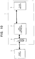
- Figure 10 illustrates a configuration of a conventional semiconductor disk device of this type.
- the semiconductor disk device inputs and outputs data from or to an external host system via an interface circuit 3.
- a CPU 4 receives the data that is input via the interface circuit 3 and writes the data into a flash memory 5.
- the CPU 4 also reads data from the flash memory 5 and outputs the data to the host system via the interface circuit 3.
- the flash memory 5 stores the above received data.
- the conventional semiconductor disk device comprises the interface circuit 3, CPU 4, and flash memory 5.
- the flash memory 5 is a non-volatile memory capable of electrically writing and erasing data. In an erasing operation, an entire data block consisting of several tens of Kbytes to several ten Kbytes is erased at one time.
- the CPU 4 also acts as a memory controller for controlling the flash memory 5.
- the semiconductor disk device 1 is connected to an external host system 11 such as a computer.
- the semiconductor disk device 1 shown in Figure 10 operates in a similar manner to that of conventional hard disk storage devices. That is, the semiconductor disk device 1 receives data from the host computer 11 and stores the received data in the flash memory 5, and reads data from the flash memory 5 according to instructions issued by the host computer 11. Unlike the conventional hard disk storage devices, however, the semiconductor disk device 1 cannot overwrite data. Therefore, it is necessary to erase the entire area of a particular block before writing data in it.
- the present invention provides a semiconductor disk device, comprising: a memory including a plurality of blocks, each block including a data storage area and an erasing-condition storage area in which an erasing condition has been written in advance; a data controller that writes data provided from the outside into the data storage area of the memory, and also reads data from the data storage area of the memory and outputs it to the outside; a power supply voltage calculating unit that compares the erasing condition stored in the erasing-condition storage area of the memory with a predefined reference condition, thereby determining a power supply voltage that minimizes the difference between the reference condition and the actual erasing condition for each block of the memory; a memory power supply unit that, in response to the output of the power supply voltage calculating unit, supplies electric power to the memory during an erasing process; and an erasing-control unit that erases data from block to block of the memory.
- Figure 1 illustrates the configuration of a semiconductor disk device according to the first embodiment.
- the semiconductor disk device inputs and outputs data from or to an external host system 11 via an interface circuit 3.
- a CPU 4 receives the data that is input via the interface circuit 3, and writes the received data into a flash memory 5, and also reads data from the flash memory 5 and outputs the data to the host system 11 via the interface circuit 3.
- the flash memory 5 stores the received data.
- a voltage control circuit 6 In response to a control signal (CONT) provided by the CPU 4, a voltage control circuit 6 generates supply voltages VCC and VPP having proper voltages and provides them to the flash memory 5.
- CONT control signal
- the flash memory 5 is a non-volatile memory capable of electrically writing and erasing data. In an erasing operation, a entire data block consisting of several Kbytes to several tens of Kbytes is erased at one time.
- the CPU 4 also acts as a memory controller for controlling the flash memory 5. Thus, the CPU 4 performs: data control in writing and reading data; erasing control in erasing data from block to block; and calculation of the supply voltage which generates the control signal (CONT) to the voltage control circuit 6.
- the above-described elements including the interface circuit 3, CPU 4, flash memory 5, and voltage control circuit 6 form the semiconductor disk device 1.
- the semiconductor disk device 1 is connected to the external host system 11 such as a computer.
- the semiconductor disk device 1 shown in Figure 1 operates in a similar manner to that of conventional hard disk storage devices. That is, the semiconductor disk device 1 receives data from the host computer 11, and stores the received data in the flash memory 5. The semiconductor disk device 1 also reads data from the flash memory 5 according to instructions issued by the host computer 11.
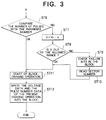
- Figures 2 and 3 are a flow chart illustrating a block-erasing process in a writing operation of the flash memory 5. For convenience of representation, the complete flow chart is divided into two portions shown in Figures 2 and 3, respectively, wherein the output A of step ST5 in Figure 2 is connected to the input A of step ST6 in Figure 3.
- Figure 4 illustrates the construction of one block of the flash memory 5 wherein the erasing of data is performed one block at a time. That is, the erasing process of the flash memory 5 is performed from block to block each having the same size as shown in Figure 4.
- the memory space of the flash memory 5 includes a plurality of blocks, wherein Figure 4 illustrates the internal organization of only one of these blocks.
- a parameter storage area 31 stores the number of pulses required for the previous erasing process, and also stores the value of the supply voltage used in that erasing process.
- a plurality of data storage areas 32 each store data received from the host system 11. Each of these data storage areas 32 corresponds to a sector that is a single unit in a writing and reading operation. Each block has one parameter storage area 31.
- the parameter storage area 31 has been initialized in advance.
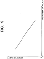
- Figure 5 is a graph illustrating the general relationship between the supply voltage applied to the flash memory and the number of erasing pulses required.
- the vertical axis of Figure 5 represents the applied voltage, and the horizontal axis represents the number of pulses required for the erasing process. As can be seen from Figure 5, the required number of erasing pulses decreases as the applied supply voltage increases.
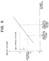
- Figure 6 illustrates a manner of determining the applied voltage required to decrease the number of erasing pulses down to a value equal to a reference number.
- the applied voltage for the next erasing operation is set to a value greater than the reference voltage by an amount ⁇ corresponding to the difference between the number of erasing pulses n in the previous erasing operation and the reference number of erasing pulses n0.
- the erasing time is maintained as a constant for all erasing blocks in the manner described below.
- the parameter storage area 31 stores the number of erasing pulses required for the erasing process in the previous writing operation.
- the CPU 4 checks whether the previous number of erasing pulses is greater than the predetermined reference number.
- the CPU 4 increases the supply voltages VCC and VPP applied to a particular block of the flash memory to be erased within a range below the maximum allowed limit, thereby reducing the number of erasing pulses to a proper value.
- the erasing operation is performed with the number of erasing pulses equal to or less than the reference number. As a result, variations in the erasing times among blocks to be erased is minimized.
- the host system 11 issues a request to write data into the flash memory
- the request is received by the CPU 4 via the interface circuit 3.
- the CPU 4 Upon receipt of the request, the CPU 4 starts its required operation.
- the CPU4 determines whether the flash memory 5 has enough free memory space to write the data requested. If enough free memory space is available (yes), there is no need to erase any block to increase the free memory space, and thus the process proceeds to step ST21 in which the data is written somewhere in the free memory space to complete the writing process.
- step ST2 determines whether the free memory space is less than the required amount (no). If it is concluded in step ST2 that the free memory space is less than the required amount (no), then the process proceeds to step ST3. This is the case, for example, when the free memory space is less than the required amount by one block.
- the CPU 4 determines the number of blocks to be erased depending on the required amount of memory space, and further determines specifically which blocks should be erased based on the number determined.
- the blocks to be erased are specified according to the following criteria: Select blocks which have been erased less times in the past than the others; Select blocks which require less erasing pulses; and Select blocks including a larger number of areas storing data already used.
- said "data already used” refers to, for example, a case in which a file is updated.
- the old data of said file that remains unchanged in a block is "data already used”.
- "data already used” is generated.
- STEP ST4 "Save Necessary Data Stored in the Block to be Erased in a Free Area"
- the CPU 4 saves the data in free memory areas, so as to prevent the data from being erased during a block-erasing operation.
- STEP ST5 "Read Voltage Data and Pulse-Number Data Associated with the Block to be Erased"
- the CPU 4 reads the data representing the number of pulses required for the previous writing operation, and also reads the data representing the voltages VCC and VPP. This data is stored in parameter storage areas 31 of the specified blocks to be erased.
- the CPU 4 compares the above read-out data representing the number of pulses of the previous erasing operation with the predetermined reference number. If these numbers are equal to each other or if the difference is within a predetermined small range (OK), then the process proceeds to step ST11 in which the block is erased.
- step ST7 If the difference is out of the above range (NG), then the process proceeds to step ST7.
- STEP ST7: " V V0 + ⁇ "
- the CPU 4 adds a certain value ⁇ to the predetermined reference voltage V0 , so as to reduce the required number of erasing pulse by increasing the voltages VCC and VPP.
- the particular value of ⁇ is determined according to the relationship shown in the graph of Figure 6.
- the graph of Figure 6 illustrates the relationship between the number of pulses of the previous erasing operation and the voltage that should be applied depending on this number.
- the graph of Figure 6 is produced from the graph shown in Figure 5 such that Figure 6 indicates the applied voltage that allows the number of erasing pulses to be equal to the reference number.
- the reference number of pulses n0 corresponds to the reference voltage V0
- the CPU 4 maintains a preinstalled table including the data representing the relationship shown in Figure 6.
- step ST8 it is determined whether the applied voltage V obtained at step ST7 is within an allowed range (defined by the specification).
- step ST11 If the applied voltage V is within the allowed range (OK), then the process proceeds to step ST11.
- the failure bits refer to particular bits that are defined in advance in the CPU 4 and that cannot be erased .
- the CPU 4 reads the sector number of the sector including a failure bit, and then the process proceeds to step ST11.
- steps ST9 and ST10 allow blocks which partially include failure bits to be used effectively.
- any block including such bits that cannot be erased is not used at all.
- failure bits exist only in a very limited part of a block. Therefore, it is possible to write data in the other sectors which include no failure bits, thereby improving the efficiency of data storage.
- the CPU 4 determines which sector is available for writing data according to the sector number that has been read in step ST10.
- the CPU 4 produces a control signal CONT based on the applied voltage determined in the steps described above, and outputs it to the voltage control circuit 7.
- the CPU 4 After applying the erasing pulses, the CPU 4 checks whether all data in the block have been successfully erased. If some data at a certain address has failed to be erased, the CPU 4 applies erasing pulses again so as to try to erase them, or if the CPU 4 acknowledges the data as a failure bit, it avoids writing data at that address.
- the CPU 4 writes the applied voltage and the number of pulses used this time in the block-erasing operation into the parameter storage area 31 of the block.
- the number of erasing pulses that was required to completely erase the block may be written in this step ST12.
- the voltages VCC and VPP applied to the flash memory are raised within the allowed range defined by the specification so that the erasing operation can be performed with a number of erasing pulses substantially equal to the reference number.
- This technique allows a block to be erased in a shorter erasing time, and also minimizes the variation of erasing times from block to block.
- the voltage control circuit 7 can vary the supply voltages (VCC, VPP) of each block of the flash memory 5 to be erased, it is therefore possible to set the supply voltages to values greater than those generally employed in conventional techniques, thereby increasing the total speed for erasing entire blocks.
- the parameter storage areas 31 are distributed through the flash memory 5 so that each block has one parameter storage area.
- the parameter storage areas 31 may also be provided separately from the data storage blocks 32 and may be concentrated in one area of the flash memory 5. Alternatively, the parameter storage areas 31 may also be disposed in the CPU 4.
- step ST12 is no longer necessary since the data, such as the number of erasing pulses, is not deleted during an erasing process.
- the number of erasing pulses and the supply voltage are given as examples of information stored in the parameter storage area 31 .
- the correction value ⁇ associated with the supply voltage that corresponds to the difference between the number of pulses required in the previous erasing operation and the reference number may also be stored therein.
- the supply voltage can be determined simply by adding the correction value ⁇ to the reference supply voltage V0 .
- the steps ST7-ST10 become simpler and thus processing speed is improved.
- the parameter storage area stores the number of pulses required in the previous erasing operation for each block. Furthermore, when an erasing operation is performed for a block that needs a number of erasing pulses greater than the predetermined reference number, the CPU raises the voltages of power supplies VCC and VPP applied to the flash memory within the allowed range defined by the specification, so that the required number of erasing pulses decreases and the variation of the erasing time from block to block is minimized.
- Figures 7 and 8 are a flow chart illustrating a block-erasing process that is required when data is written in the flash memory 5. For convenience of representation, the complete flow chart is divided into two portions shown in Figures 7 and 8, respectively, wherein the output B of step ST13 or ST14 in Figure 7 is the input B of step ST6 in Figure 8.
- Figures 7 and 8 are similar to Figures 2 and 3 except that the flow chart given by Figures 7 and 8 includes steps ST13 and ST15.
- Figure 9 illustrates the organization of one block of the flash memory 5 wherein the erasing of data is performed from block to block. As in the first embodiment, the erasing process of the flash memory 5 is performed from block to block wherein each block has a fixed size.
- the memory space of the flash memory 5 includes a plurality of blocks, and Figure 9 illustrates the arrangement of one of these blocks.
- a parameter storage area 31 stores the number of pulses required in the previous erasing process, and also stores the value of the supply voltage used in that erasing process.
- Data storage areas 32 store data received from the host system 11. Each of these data storage areas 32 corresponds to a sector, that is, a unit in writing and reading operation. Each block has one parameter storage area 31. The block also includes flag areas 33 wherein one flag area 33 is provided for one corresponding data storage area 32. These flag areas 33 are used to disable corresponding data storage areas 32 as required.
- the general configuration of the semiconductor disk device is the same as that shown in Figure 1.
- the CPU 4 sets a failure-bit flag in a flag area 33 corresponding to a failed sector of the block. According to the failure bits that have been set, the CPU 4 writes data in data storage areas 32 other than those corresponding to the failure bits.
- steps ST1 through ST5 are the same as those in embodiment 1 that has already been described, these steps are not described in the following description.
- step ST5 "Read Voltage Data and Pulse Number Data Associated with the Block to be Erased"
- the data associated with the number of pulses required in the previous erasing process as well as the data associated with voltages of power supply VCC and VPP is read, and then the process proceeds to step ST13.
- the CPU 4 checks the flag areas 33 in the block to be erased to determine whether there is a sector to which a disable flag is set. If there is no such a sector (no), then the process proceeds to step ST6.
- step ST14 If some sectors are disabled (yes), then the process proceeds to step ST14.
- the CPU 4 stores which sectors (data storage areas 32) are disabled.
- step ST6 The process next proceeds to step ST6.
- the CPU 4 compares the above read-out data representing the number of pulses of the previous erasing operation with the predetermined reference number. If these numbers are equal to each other or the difference is within a predetermined small range, then the process proceeds to step ST11 in which the block is erased.
- the CPU 4 adds a certain value a to the predetermined reference voltage V0 , so as to reduce the required number of erasing pulse by increasing the voltages VCC and VPP.
- a particular correction value ⁇ is determined in the same manner as in the first embodiment.
- the CPU 4 determines whether the applied voltage V obtained in step ST7 is within an allowed range (defined by the specification).
- step ST11 If the applied voltage V is within the allowed range (OK), then the process proceeds to step ST11.
- the failure bits refer to particular bits that cannot be erased and the information about which is stored in advance in the CPU 4.
- the CPU 4 reads the sector number of a sector including a failure bit, and then the process proceeds to step ST16.
- steps ST9 and ST10 allow blocks which partially include failure bits to be used effectively.
- the CPU 4 produces a control signal CONT based on the applied voltage determined in the previous steps, and outputs it to the voltage control circuit 7.
- the CPU 4 After applying the erasing pulses, the CPU 4 checks whether all data in the block have been successfully erased. However, if it has been concluded in steps ST13 and ST14 that some disable flags indicate the presence of disabled sectors, the CPU 4 does not per form verification on these sectors because these sectors will not be used.
- the CPU 4 writes the applied voltage and the number of pulses used in the block-erasing operation at this time into the parameter storage area 31 of the block.
- the CPU 4 rewrites the disable data that has been stored in advance in the flag areas 33 into the flag areas 33 of the block. This is necessary because the flag areas 33 are also erased during the block-erasing operation, and thus it is required to rewrite the disable data in the flag areas 33.
- an arbitrary data storage area 32 can be disabled by writing disable data in the corresponding flag area 33.
- This technique allows a block to be erased in a shorter erasing time, and also minimizes the variations of the erasing times from block to block even in the case where there is a bit that cannot be erased by the allowable maximum supply voltage.
- the CPU 4 can know in advance which sectors are disabled by reading disable flags, and therefore it is possible to skip processing sectors including a failure bit during the block-erasing operation of the flash memory. This results in a higher operation speed in the next block-erasing operation.
- the flag areas 33 are distributed through the flash memory 5 so that each block has it own flag areas.
- the flag areas 33 may also be provided separately from the data storage blocks 32 and may be concentrated in one area of the flash memory. Alternatively, the flag areas 33 may also be disposed at proper locations in the CPU 4.
- step ST15 is no longer needed since the disable flag is not deleted during an erasing process.
- a semiconductor disk device provided with a flash memory capable of performing a stable block erasing operation in a short time period wherein the variations in the erasing times from block to block are minimized.
- the semiconductor disk device includes: a flash memory (5) including a data storage area and an erasing-condition storage area in which an erasing condition has been written in advance; a CPU (4) acting as a memory controller; and a voltage controlling circuit (6) for changing applied voltages VCC and VPP under the control of the CPU (4).
- the CPU (4) has the power supply voltage calculating capability of comparing the erasing condition stored in the erasing-condition storage area of the flash memory (5) with a predetermined reference condition, and determining an optimal power supply voltage for each block so that the actual erasing time for each block becomes equal to a minimized constant value.
Landscapes
- Engineering & Computer Science (AREA)
- Theoretical Computer Science (AREA)
- Human Computer Interaction (AREA)
- Physics & Mathematics (AREA)
- General Engineering & Computer Science (AREA)
- General Physics & Mathematics (AREA)
- Read Only Memory (AREA)
- Techniques For Improving Reliability Of Storages (AREA)
Applications Claiming Priority (3)
| Application Number | Priority Date | Filing Date | Title |
|---|---|---|---|
| JP6250786A JPH08115597A (ja) | 1994-10-17 | 1994-10-17 | 半導体ディスク装置 |
| JP25078694 | 1994-10-17 | ||
| JP250786/94 | 1994-10-17 |
Publications (3)
| Publication Number | Publication Date |
|---|---|
| EP0708450A2 true EP0708450A2 (de) | 1996-04-24 |
| EP0708450A3 EP0708450A3 (de) | 1998-09-02 |
| EP0708450B1 EP0708450B1 (de) | 2000-06-28 |
Family
ID=17213034
Family Applications (1)
| Application Number | Title | Priority Date | Filing Date |
|---|---|---|---|
| EP95104653A Expired - Lifetime EP0708450B1 (de) | 1994-10-17 | 1995-03-29 | Halbleiterplattenvorrichtung mit konstanter Dateneinschreibzeitperiode |
Country Status (4)
| Country | Link |
|---|---|
| US (1) | US5619452A (de) |
| EP (1) | EP0708450B1 (de) |
| JP (1) | JPH08115597A (de) |
| DE (1) | DE69517649T2 (de) |
Cited By (3)
| Publication number | Priority date | Publication date | Assignee | Title |
|---|---|---|---|---|
| WO1997017704A3 (de) * | 1995-11-10 | 1997-06-26 | Siemens Ag | Verfahren und vorrichtung zum selbsttätigen ermitteln der nötigen hochspannung zum programmieren/löschen eines eeproms |
| US6052306A (en) * | 1996-11-04 | 2000-04-18 | Siemens Aktiengesellschaft | Method and device for automatic determination of the required high voltage for programming/erasing an EEPROM |
| DE10192507B4 (de) * | 2000-06-06 | 2010-05-06 | Intel Corporation, Santa Clara | Verfahren und Vorrichtung für die Vorhersage von Lösch- und Schreibzeiten von Flash-Speichern |
Families Citing this family (23)
| Publication number | Priority date | Publication date | Assignee | Title |
|---|---|---|---|---|
| US5893135A (en) * | 1995-12-27 | 1999-04-06 | Intel Corporation | Flash memory array with two interfaces for responding to RAS and CAS signals |
| JPH09244961A (ja) * | 1996-03-08 | 1997-09-19 | Mitsubishi Electric Corp | フラッシュata−pcカード |
| US5717632A (en) * | 1996-11-27 | 1998-02-10 | Advanced Micro Devices, Inc. | Apparatus and method for multiple-level storage in non-volatile memories |
| JPH10177563A (ja) * | 1996-12-17 | 1998-06-30 | Mitsubishi Electric Corp | フラッシュメモリ内蔵マイクロコンピュータ |
| US5748537A (en) * | 1997-02-13 | 1998-05-05 | Garbers; Jeffrey Paul | Method and apparatus for storing items in flash memory |
| KR100701049B1 (ko) * | 2000-05-17 | 2007-03-29 | 현대아이티주식회사 | 전기/전자기기내 이이피롬의 보호방법 |
| US6704835B1 (en) * | 2000-09-26 | 2004-03-09 | Intel Corporation | Posted write-through cache for flash memory |
| JP4124557B2 (ja) * | 2000-10-05 | 2008-07-23 | 松下電器産業株式会社 | 半導体集積回路装置及びその制御方法 |
| US7178004B2 (en) | 2003-01-31 | 2007-02-13 | Yan Polansky | Memory array programming circuit and a method for using the circuit |
| US7535765B2 (en) | 2004-12-09 | 2009-05-19 | Saifun Semiconductors Ltd. | Non-volatile memory device and method for reading cells |
| CN1838323A (zh) * | 2005-01-19 | 2006-09-27 | 赛芬半导体有限公司 | 可预防固定模式编程的方法 |
| US7808818B2 (en) | 2006-01-12 | 2010-10-05 | Saifun Semiconductors Ltd. | Secondary injection for NROM |
| US7638835B2 (en) | 2006-02-28 | 2009-12-29 | Saifun Semiconductors Ltd. | Double density NROM with nitride strips (DDNS) |
| US20070255889A1 (en) * | 2006-03-22 | 2007-11-01 | Yoav Yogev | Non-volatile memory device and method of operating the device |
| US20080049512A1 (en) * | 2006-08-23 | 2008-02-28 | Konrad Seidel | Nonvolatile memory device and method of programming the same |
| US7605579B2 (en) | 2006-09-18 | 2009-10-20 | Saifun Semiconductors Ltd. | Measuring and controlling current consumption and output current of charge pumps |
| KR100843037B1 (ko) * | 2007-03-27 | 2008-07-01 | 주식회사 하이닉스반도체 | 플래시 메모리 장치 및 이의 소거 방법 |
| US20080239599A1 (en) * | 2007-04-01 | 2008-10-02 | Yehuda Yizraeli | Clamping Voltage Events Such As ESD |
| US7590001B2 (en) | 2007-12-18 | 2009-09-15 | Saifun Semiconductors Ltd. | Flash memory with optimized write sector spares |
| US7971023B2 (en) * | 2008-04-30 | 2011-06-28 | Sandisk Corporation | Guaranteed memory card performance to end-of-life |
| WO2012001917A1 (ja) * | 2010-06-29 | 2012-01-05 | パナソニック株式会社 | 不揮発性記憶システム、メモリシステム用の電源回路、フラッシュメモリ、フラッシュメモリコントローラ、および不揮発性半導体記憶装置 |
| KR102775181B1 (ko) | 2018-12-07 | 2025-03-04 | 삼성전자주식회사 | 스토리지 시스템 및 스토리지 시스템의 동작 방법 |
| US12271618B2 (en) * | 2022-10-24 | 2025-04-08 | Micron Technology, Inc. | Identifying center of valley in memory systems |
Family Cites Families (5)
| Publication number | Priority date | Publication date | Assignee | Title |
|---|---|---|---|---|
| DE69024086T2 (de) * | 1989-04-13 | 1996-06-20 | Sundisk Corp | EEprom-System mit Blocklöschung |
| US5065364A (en) * | 1989-09-15 | 1991-11-12 | Intel Corporation | Apparatus for providing block erasing in a flash EPROM |
| JPH0447595A (ja) * | 1990-06-15 | 1992-02-17 | Mitsubishi Electric Corp | 不揮発性半導体記憶装置 |
| JPH0750558B2 (ja) * | 1992-09-22 | 1995-05-31 | インターナショナル・ビジネス・マシーンズ・コーポレイション | 一括消去型不揮発性メモリ |
| US5485595A (en) * | 1993-03-26 | 1996-01-16 | Cirrus Logic, Inc. | Flash memory mass storage architecture incorporating wear leveling technique without using cam cells |
-
1994
- 1994-10-17 JP JP6250786A patent/JPH08115597A/ja active Pending
-
1995
- 1995-03-29 EP EP95104653A patent/EP0708450B1/de not_active Expired - Lifetime
- 1995-03-29 DE DE69517649T patent/DE69517649T2/de not_active Expired - Fee Related
- 1995-04-27 US US08/429,773 patent/US5619452A/en not_active Expired - Fee Related
Cited By (3)
| Publication number | Priority date | Publication date | Assignee | Title |
|---|---|---|---|---|
| WO1997017704A3 (de) * | 1995-11-10 | 1997-06-26 | Siemens Ag | Verfahren und vorrichtung zum selbsttätigen ermitteln der nötigen hochspannung zum programmieren/löschen eines eeproms |
| US6052306A (en) * | 1996-11-04 | 2000-04-18 | Siemens Aktiengesellschaft | Method and device for automatic determination of the required high voltage for programming/erasing an EEPROM |
| DE10192507B4 (de) * | 2000-06-06 | 2010-05-06 | Intel Corporation, Santa Clara | Verfahren und Vorrichtung für die Vorhersage von Lösch- und Schreibzeiten von Flash-Speichern |
Also Published As
| Publication number | Publication date |
|---|---|
| JPH08115597A (ja) | 1996-05-07 |
| DE69517649D1 (de) | 2000-08-03 |
| US5619452A (en) | 1997-04-08 |
| EP0708450A3 (de) | 1998-09-02 |
| DE69517649T2 (de) | 2001-03-01 |
| EP0708450B1 (de) | 2000-06-28 |
Similar Documents
| Publication | Publication Date | Title |
|---|---|---|
| US5619452A (en) | Semiconductor disk device with a constant data-writing time period | |
| EP0675502B1 (de) | EEPROM-System mit aus mehreren Chips bestehender Blocklöschung | |
| US5715193A (en) | Flash memory system and method for monitoring the disturb effect on memory cell blocks due to high voltage conditions of other memory cell blocks | |
| US5754567A (en) | Write reduction in flash memory systems through ECC usage | |
| US5920501A (en) | Flash memory system and method for monitoring the disturb effect on memory cell blocks due to high voltage conditions of other memory cell blocks | |
| US5530827A (en) | Data management system for programming-limited type semiconductor memory and IC memory card employing data save/erase process with flag assignment | |
| US5937424A (en) | Method and apparatus for suspending the writing of a nonvolatile semiconductor memory with program suspend command | |
| US5841699A (en) | Storage device and method to detect its degradation | |
| KR101423612B1 (ko) | 불휘발성 메모리 장치 및 그것의 동작 방법, 그리고 그것을포함하는 메모리 시스템 | |
| US7046558B2 (en) | Method for controlling a nonvolatile memory | |
| US8391067B2 (en) | Nonvolatile memory | |
| US5802553A (en) | File system configured to support variable density storage and data compression within a nonvolatile memory | |
| US20020178338A1 (en) | Non-volatile data storage system and data storaging method | |
| US11507272B2 (en) | Controller for performing garbage collection operation based on performance ratio and memory system including the same | |
| US20150261669A1 (en) | Devices and methods for operating a solid state drive | |
| EP1739683A1 (de) | Platzverwaltung zur Verwaltung eines nichtflüchtigen Hochleistungsspeichers | |
| EP1729304A1 (de) | Platzverwaltung zur Verwaltung eines nichtflüchtigen Hochleistungsspeichers | |
| JP3098486B2 (ja) | 不揮発性半導体記憶装置 | |
| US20050138271A1 (en) | Rotational use of memory to minimize write cycles | |
| EP1839154A1 (de) | System und verfahren zum löschen von nichtflüchtigen aufzeichnungsmedien | |
| US6189070B1 (en) | Apparatus and method for suspending operation to read code in a nonvolatile writable semiconductor memory | |
| US6457093B2 (en) | Circuit and method to control operations of another circuit | |
| KR20230169733A (ko) | 메모리 장치 동작 방법 | |
| US6898680B2 (en) | Minimization of overhead of non-volatile memory operation | |
| US7054198B2 (en) | Flash memory with fast boot block access |
Legal Events
| Date | Code | Title | Description |
|---|---|---|---|
| PUAI | Public reference made under article 153(3) epc to a published international application that has entered the european phase |
Free format text: ORIGINAL CODE: 0009012 |
|
| AK | Designated contracting states |
Kind code of ref document: A2 Designated state(s): DE FR GB |
|
| PUAL | Search report despatched |
Free format text: ORIGINAL CODE: 0009013 |
|
| AK | Designated contracting states |
Kind code of ref document: A3 Designated state(s): DE FR GB |
|
| 17P | Request for examination filed |
Effective date: 19981009 |
|
| 17Q | First examination report despatched |
Effective date: 19981125 |
|
| GRAG | Despatch of communication of intention to grant |
Free format text: ORIGINAL CODE: EPIDOS AGRA |
|
| GRAG | Despatch of communication of intention to grant |
Free format text: ORIGINAL CODE: EPIDOS AGRA |
|
| GRAH | Despatch of communication of intention to grant a patent |
Free format text: ORIGINAL CODE: EPIDOS IGRA |
|
| GRAH | Despatch of communication of intention to grant a patent |
Free format text: ORIGINAL CODE: EPIDOS IGRA |
|
| GRAA | (expected) grant |
Free format text: ORIGINAL CODE: 0009210 |
|
| AK | Designated contracting states |
Kind code of ref document: B1 Designated state(s): DE FR GB |
|
| REF | Corresponds to: |
Ref document number: 69517649 Country of ref document: DE Date of ref document: 20000803 |
|
| ET | Fr: translation filed | ||
| PLBE | No opposition filed within time limit |
Free format text: ORIGINAL CODE: 0009261 |
|
| STAA | Information on the status of an ep patent application or granted ep patent |
Free format text: STATUS: NO OPPOSITION FILED WITHIN TIME LIMIT |
|
| 26N | No opposition filed | ||
| REG | Reference to a national code |
Ref country code: GB Ref legal event code: IF02 |
|
| PGFP | Annual fee paid to national office [announced via postgrant information from national office to epo] |
Ref country code: FR Payment date: 20030310 Year of fee payment: 9 |
|
| PGFP | Annual fee paid to national office [announced via postgrant information from national office to epo] |
Ref country code: GB Payment date: 20030326 Year of fee payment: 9 |
|
| PGFP | Annual fee paid to national office [announced via postgrant information from national office to epo] |
Ref country code: DE Payment date: 20030409 Year of fee payment: 9 |
|
| PG25 | Lapsed in a contracting state [announced via postgrant information from national office to epo] |
Ref country code: GB Free format text: LAPSE BECAUSE OF NON-PAYMENT OF DUE FEES Effective date: 20040329 |
|
| PG25 | Lapsed in a contracting state [announced via postgrant information from national office to epo] |
Ref country code: DE Free format text: LAPSE BECAUSE OF NON-PAYMENT OF DUE FEES Effective date: 20041001 |
|
| GBPC | Gb: european patent ceased through non-payment of renewal fee |
Effective date: 20040329 |
|
| PG25 | Lapsed in a contracting state [announced via postgrant information from national office to epo] |
Ref country code: FR Free format text: LAPSE BECAUSE OF NON-PAYMENT OF DUE FEES Effective date: 20041130 |
|
| REG | Reference to a national code |
Ref country code: FR Ref legal event code: ST |