EP0708531A1 - Digital-to-analog converter with reduced number of resistors - Google Patents
Digital-to-analog converter with reduced number of resistors Download PDFInfo
- Publication number
- EP0708531A1 EP0708531A1 EP95307181A EP95307181A EP0708531A1 EP 0708531 A1 EP0708531 A1 EP 0708531A1 EP 95307181 A EP95307181 A EP 95307181A EP 95307181 A EP95307181 A EP 95307181A EP 0708531 A1 EP0708531 A1 EP 0708531A1
- Authority
- EP
- European Patent Office
- Prior art keywords
- analog
- digital
- output
- output node
- switching
- Prior art date
- Legal status (The legal status is an assumption and is not a legal conclusion. Google has not performed a legal analysis and makes no representation as to the accuracy of the status listed.)
- Withdrawn
Links
Images
Classifications
-
- H—ELECTRICITY
- H03—ELECTRONIC CIRCUITRY
- H03M—CODING; DECODING; CODE CONVERSION IN GENERAL
- H03M1/00—Analogue/digital conversion; Digital/analogue conversion
- H03M1/66—Digital/analogue converters
-
- H—ELECTRICITY
- H03—ELECTRONIC CIRCUITRY
- H03M—CODING; DECODING; CODE CONVERSION IN GENERAL
- H03M1/00—Analogue/digital conversion; Digital/analogue conversion
- H03M1/66—Digital/analogue converters
- H03M1/74—Simultaneous conversion
- H03M1/76—Simultaneous conversion using switching tree
- H03M1/765—Simultaneous conversion using switching tree using a single level of switches which are controlled by unary decoded digital signals
Definitions
- This invention relates generally to integrated circuits having digital-to-analog converters (DACs), and more particularly to such converters requiring fewer resistors in a resistance string to achieve a given level of resolution than were required by prior art DACs.
- DACs digital-to-analog converters
- DACs are used to convert a digitally coded signal to an analog signal, or in conjunction with successive approximation circuitry as part of an analog-to-digital converter.
- DACs convert a digitally coded signal to an analog signal that is proportional to the digital signal.
- the analog signal can take on many different values depending on the resolution.
- the range of analog values is predetermined and corresponds to the range of digitally coded signals.
- DACs may employ a single resistor string comprised of equal resistance resistors.
- the resistor string has intermediate taps between adjacent resistors in the resistor string as well as between the resistor string and an energy source energizing the resistor string. Switches, coupled between respective intermediate taps and an output node, when turned on electrically couple the intermediate tap to the output node, and isolate the intermediate tap from the output node when turned off.
- a digitally encoded signal is provided to a decoding/driver circuit.
- the decoding circuit decodes the digitally encoded signal and turns on the appropriate switch to conduct the voltage at its associated intermediate tap to the output. Typically only a single switch is turned on at a time, resulting in a single intermediate tap being coupled to the output.
- a monotonic input-output characteristic that is a staircase output voltage is derived from the resistor-division voltage at the intermediate taps. The magnitude of the incremental steps in the output voltage is the voltage drop across one of the resistors of the resistor string.
- a digital-to-analog converter includes a resistor string having intermediate taps. Switching transistors are coupled between an output node and respective intermediate taps. Decode circuits for decoding a digitally coded signal are capable of switching at least two transistors to be in the on state simultaneously to generate at least some of the analog voltages. Having at least two transistors switched to the on state electrically couples more than one intermediate tap to the output node to generate a single analog signal.
- one row select line can be energized simultaneously with at least two column select lines.
- at least two column select lines can be energized simultaneously with one row select line.
- the DAC also may be used with successive approximation circuitry to provide an analog-to-digital converter.
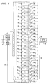
- DAC 10 includes a resistor string coupled between two potential values and energized by an energy source. Switches controlled by a selection and driver circuit couple intermediate taps to a common output node. The magnitude of an analog voltage appearing at the output node depends on which switch or switches are activated. The output is amplified by an output amplifier.
- a DAC in accordance with the present invention is suitable for fabrication in the form of a monolithic integrated circuit.
- Resistor string 12 is comprised of a number, n, of resistors of equal resistance in series.
- the resistors are denoted R1 through R n .
- resistor string 12 is a thin film metal resistor network on a silicon layer.
- Resistor string 12 is coupled across and energized by energy source 4, which may be either a voltage or a current source.
- energy source 4 which may be either a voltage or a current source.
- the resistance values of the resistors comprising the resistor string are application dependent and will be readily selected based on a variety of parameters such as the power to be dissipated, the potential across the resistor string, and the number of resistors in the resistor string.
- V1 may be substantially the power supply voltage
- V2 may be ground potential as provided by energy source 4.
- switches are coupled between an output node 14 and a respective junction. These junctions are referred to as intermediate taps.
- a switch shown in the illustrative embodiment as a MOS transistor, is coupled between a respective intermediate tap and output node 14.
- Transistors M2 through M n are coupled between the output node and intermediate taps T2 through T n , which are between contiguous resistors in the resistor string.
- Transistor M1 is coupled between potential V1 and output node 14, thereby defining intermediate tap T1.
- Transistor M n+1 is coupled between potential V2 and output node 14, thereby defining intermediate tap T n+1 .
- Transistors M1 through M n+1 each couple a respective intermediate tap, T1 through T n+1 , with output node 14.
- the transistors M1 through M n+1 are switching transistors that are nominally identical and have an impedance in the conductive state that is very large compared to the resistance of resistors R1 through R n in resistor string 12.
- the conductive impedance of the switching transistors is on the order of 1,000 to 10,000 ohms.
- Output amplifier 18 amplifies the output signal at output node 14 and may convert the output to another form, such as from a voltage output to a current output.
- the switching transistors M1 through M n+1 are controlled by switching transistor selection and driver circuit 2.
- Switching transistor selection and driver circuit 2 receives a digitally coded input 6 and, as described in more detail below, switches on selective ones of the switching transistors.
- two or more transistors M1 through M n+1 can be switched to simultaneously be in the on state.
- This provides an output with a resolution, defined as the smallest change that can occur in the analog output as a result of a change in the digital input, that is smaller than the differential voltage across individual resistors R1 through R n that comprise resistor string 12.
- two intermediate taps are electrically coupled to output node 14.
- the analog voltage appearing at output node 14 is an intermediate voltage that is substantially halfway between the voltages at the intermediate taps electrically coupled to the output node.
- the switching transistors turned on to electrically couple the intermediate taps to the output node are also adjacent to each other.
- the invention is not so limited.
- the switching transistors need not be adjacent, and the intermediate taps coupled to the output node need not be adjacent.
- the number of resistors in a resistor string can be reduced by half with the percentage resolution of a DAC maintained.
- the number of resistors in a resistor string and the number of switching transistors can be reduced by half without the number of possible levels in the analog output being reduced.
- Half of the possible levels in the analog output require a single transistor to be switched on to electrically couple a voltage at an intermediate tap to the output node.
- the other half of the possible levels in the analog output require two transistors to be switched on so that a voltage between the voltage at the two intermediate taps electrically coupled to the output node is provided at output node 14.
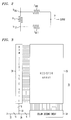
- the resulting equivalent circuit is shown in Figure 2. Since the impedance of the transistors M16 and M17, represented as Z M16 and Z M17 , are substantially identical and large compared to R16, the voltage at output node 14 is substantially halfway between the voltage at intermediate taps T16 and T17. A small error is present, but it is acceptable as a trade-off for the substantial reduction in both the number of resistors in the resistor string and the number of switching transistors, and hence a reduction in the area of silicon required to fabricate the resistor string and switching transistors in an integrated circuit.
- FIG. 3 shows schematically the construction of a DAC in accordance with an illustrative embodiment of the present invention.
- DAC 10 is configured like a memory with row and column decoding circuits to select the transistor or transistors to turn on and hence generate the desired analog output voltage that corresponds to a digital input to the DAC.
- FIG. 3 represents a 16 bit DAC.
- Switching transistor selection and driver circuit 2 is shown comprising row decoding circuit 24 and column decoding circuit 28.
- Bus 20 delivers 16 bits to DAC 10. Eight of the 16 bits are provided on bus 22, a subset of bus 20, to row decoding circuit 24. The remaining 8 bits are provided on bus 26, also a subset of bus 20, to column decoding circuit 28.
- Row decoding circuit 24 and column decoding circuit 28 are combinatorial logic. Such combinatorial logic can be designed by one of ordinary skill in the art to decode the bits received and drive one or more rows or columns.
- each decoding circuit eight bits are received by each decoding circuit.
- the eight bits received by row decoding circuit 24 are decoded to determine which one of 28, or 256, row select lines to activate.
- the eight bits received by column decoding circuit 28 are decoded to determine which one or two of 27, or 128, column select lines to activate.
- One possible convention used to determine which additional intermediate tap is electrically coupled to output node 14 is described in greater detail below.
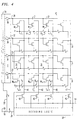
- resistor array 30 An illustrative portion of resistor array 30 is shown in greater detail in the schematic diagram of Figure 4.
- Resistor string 12 is positioned in the region of resistor array 30 arranged in an array of one less than 256 x 128 resistor selecting cells 31, with a fixed resistance per cell.
- a row select line driver 32, 34, 36, or 38 within row decoding circuit 24 energizes a respective row select line 33, 35, 37, or 39 to energize the gate of each transistor in a row of cells.
- column decoding circuit 28 Similarly, the eight bit binary input to column decoding circuit 28 is decoded. Based on seven of the eight bits, a column select line driver 40, 42, 44 or 46 within column decoding circuit 28 energizes a respective column select line 41, 43, 45, or 47 to couple the source of the switching transistors in a column of cells to output node 14. The eighth bit is decoded by the column decoding circuit 28 to turn on a second column select line driver 40, 42, 44, or 46.
- At the intersection of a row of cells having the switching transistor gate energized by a row select line, and a column of cells having the switching transistor source coupled to output node 14 is a cell in which the transistor gate is energized and the transistor source is coupled to the output. In this cell, the intermediate tap is coupled to output node 14.
- either another column select line driver 40, 42, 44 or 46 is energized or another row select line driver 32, 34, 36 or 38 is energized.
- a second column select line driver is energized to also couple an adjacent intermediate tap in resistor string 12 to output node 14.
- row select line driver 38 and column select line driver 42 are energized coupling intermediate tap T2 to output node 14
- either column select line driver 40 or 44 could be energized.
- Energizing column select line driver 40 energizes column select line 41 to also couple intermediate tap T1 to output node 14 whereas energizing column select line driver 44 energizes column select line 45 to also couple intermediate tap T3 to output node 14.
- the analog output voltage at output node 14 or output from output amplifier 18 is a stepwise linear function.
- the largest analog voltage is achieved by coupling intermediate tap T1 to the output node 14.
- the stepwise voltage levels decreasing in magnitude at output node 14 are then achieved by electrically coupling to output node 14 intermediate taps T1 and T2, T2, T2 and T3, T3, T3 and T4, T4 etc.
- One less than half of the analog voltage levels requires that two intermediate taps be simultaneously electrically coupled to output node 14 to generate the desired analog voltage.
- the eight bits received by column decoding circuit 28 are decoded to determine which one or more of the 128 column select lines to activate.
- Seven of the eight bits determine whether one column select line is to be activated or whether two lines are to be activated. A convention is used to determine which additional column select line to activate and hence which additional intermediate tap is electrically coupled to output node 14. An example showing which intermediate taps are electrically coupled to output node 14 for several eight bit sequences is shown in Table I. The pattern is evident and can be continued for the remaining eight bit sequences. Other conventions are possible.
- row decoding circuit 24 and column decoding circuit 28 are designed to identify these occurrences and energize the appropriate column and row select lines to produce the desired analog output voltage at output node 14.
- Such a DAC provides 216 or 65,536 possible output valves.
- Prior art DACs would require substantially 65,536 resistors and 65,536 switching transistors to achieve the same degree of resolution.
- the ability to switch on two or more switching transistors to be in the on state simultaneously to generate at least some of the analog values reduces the number of resistors and the number of switching transistors by half or more and still achieves the same degree of resolution in the analog output.
- the silicon area required to fabricate the resistor string and switching transistors is reduce by half or more.
- Settling time is defined as the amount of time required to charge parasitic capacitance up to a relatively steady state value.
- Output node 14 has some parasitic capacitance with respect to ground.
- the power to charge the parasitic capacitance is provided by energy source 4 energizing potential V1.
- the power passes through a portion of the resistor string and switching transistors. With multiple switching transistors switched to the on state and a corresponding reduction in the number of resistors required in the resistor string, the parasitic capacitance can be charged in less time.
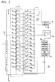
- An analog-to-digital converter 100 incorporating a digital-to-analog converter in accordance with the illustrative embodiment of the invention, is shown in Figure 4.
- An analog signal 102 is received and provides the positive input to comparator 104.
- the successive approximation circuitry 106 turns on the appropriate switching transistor or transistors M1 though M17 to produce the midpoint voltage of resistor string 112 at node 114.
- the voltage at node 114 provides the input to output amplifier 118 which may amplify the signal it receives and may convert the signal to another form, such as from a voltage output to a current output.
- the output 130 of output amplifier 118 provides the negative input to comparator 104.
- Comparator 104 compares the output 130 of output amplifier 118, which is a generated analog signal, to analog signal 102 which may be maintained on a sample-and-hold circuit.
- Successive approximation circuitry 106 initially turns on the appropriate switching transistor or transistors M1 through M17 to produce the midpoint voltage of resistor string 112 as analog signal 130. If the output 132 is positive, the midpoint of the upper half of the resistor string 112 is electrically coupled as the input to comparator 104 and compared to analog signal 102. If the output 132 is negative, the midpoint of the lower half of the resistor string 112 is electrically coupled as the input to output amplifier 118 and compared to analog signal 102. The selection of the switching transistor or transistors that are switched on, as described above, are controlled by successive approximation circuitry 106.
- each iteration determines one bit in the binary, or other coded, representation 134, and the successive approximation process continues until all bits are determined.
- the successive approximation process is similar to known successive approximation processes but differs in that one or more switching transistors may be switched to the on state to couple a midpoint voltage as an input to comparator 104 where the midpoint voltages are not limited to being voltages at the intermediate taps.
- the binary representation 134 is provided as the output of successive approximation circuitry 106 and analog-to-digital converter 100.
- the invention is particularly useful in communication systems and equipment employing integrated circuits in digital-to-analog and analog-to-digital converter applications.
- Such communication systems and equipment have the advantage of maintaining resolution while reducing silicon area requirements by reducing the number of resistors and switching transistors and improving settling time.
Landscapes
- Engineering & Computer Science (AREA)
- Theoretical Computer Science (AREA)
- Analogue/Digital Conversion (AREA)
- Semiconductor Integrated Circuits (AREA)
Applications Claiming Priority (2)
| Application Number | Priority Date | Filing Date | Title |
|---|---|---|---|
| US327174 | 1994-10-21 | ||
| US08/327,174 US5604501A (en) | 1994-10-21 | 1994-10-21 | Digital-to-analog converter with reduced number of resistors |
Publications (1)
| Publication Number | Publication Date |
|---|---|
| EP0708531A1 true EP0708531A1 (en) | 1996-04-24 |
Family
ID=23275467
Family Applications (1)
| Application Number | Title | Priority Date | Filing Date |
|---|---|---|---|
| EP95307181A Withdrawn EP0708531A1 (en) | 1994-10-21 | 1995-10-11 | Digital-to-analog converter with reduced number of resistors |
Country Status (6)
| Country | Link |
|---|---|
| US (1) | US5604501A (ja) |
| EP (1) | EP0708531A1 (ja) |
| JP (1) | JPH08237128A (ja) |
| KR (1) | KR960016160A (ja) |
| CN (1) | CN1122973A (ja) |
| TW (1) | TW269076B (ja) |
Cited By (2)
| Publication number | Priority date | Publication date | Assignee | Title |
|---|---|---|---|---|
| KR100502402B1 (ko) * | 1997-09-04 | 2005-10-12 | 삼성전자주식회사 | 축차비교형아날로그-디지탈변환회로 |
| EP3086309A4 (en) * | 2013-12-19 | 2017-08-09 | Boe Technology Group Co. Ltd. | Ramp signal generation circuit and signal generator, array substrate and display device |
Families Citing this family (27)
| Publication number | Priority date | Publication date | Assignee | Title |
|---|---|---|---|---|
| US5977897A (en) * | 1996-12-31 | 1999-11-02 | Lucent Technologies Inc. | Resistor string with equal resistance resistors and converter incorporating the same |
| US5969657A (en) * | 1997-07-22 | 1999-10-19 | Analog Devices, Inc. | Digital to analog converter |
| US5977898A (en) * | 1997-12-22 | 1999-11-02 | Texas Instruments Incorporated | Decoding scheme for a dual resistor string DAC |
| US6225929B1 (en) | 1998-12-02 | 2001-05-01 | Hewlett-Packard Company | Digital-to-analog converter having switchable current sources and resistor string |
| US6529152B1 (en) * | 1999-10-15 | 2003-03-04 | Cyngal Integrated Products, Inc. | High precision SAR converter using resistor strip with auto zeroing function |
| US6356222B1 (en) * | 2000-05-04 | 2002-03-12 | Matsushita Mobile Communication Development Corporation Of Usa | Circuit to increase the precision of a digital-to-analog converter |
| EP1346467B1 (en) * | 2000-11-29 | 2010-02-10 | Broadcom Corporation | Integrated direct conversion satellite tuner |
| KR100495500B1 (ko) * | 2000-12-14 | 2005-06-17 | 매그나칩 반도체 유한회사 | 디지털/아날로그 변환기 |
| US6507272B1 (en) * | 2001-07-26 | 2003-01-14 | Maxim Integrated Products, Inc. | Enhanced linearity, low switching perturbation resistor string matrices |
| JP2005516441A (ja) * | 2002-01-24 | 2005-06-02 | コーニンクレッカ フィリップス エレクトロニクス エヌ ヴィ | 電流信号を電圧信号に変換する電子回路 |
| JP2003318264A (ja) * | 2002-04-19 | 2003-11-07 | Rohm Co Ltd | 出力特性可変型半導体集積回路装置 |
| JP4002147B2 (ja) * | 2002-07-24 | 2007-10-31 | 沖電気工業株式会社 | ディジタル/アナログ変換回路 |
| US6842135B2 (en) * | 2003-02-15 | 2005-01-11 | Stmicroelectronics Limited | Ramp generator |
| US6911896B2 (en) * | 2003-03-31 | 2005-06-28 | Maxim Integrated Products, Inc. | Enhanced linearity, low switching perturbation resistor strings |
| US7154346B2 (en) * | 2004-07-30 | 2006-12-26 | Broadcom Corporation | Apparatus and method to provide a local oscillator signal |
| US7535976B2 (en) * | 2004-07-30 | 2009-05-19 | Broadcom Corporation | Apparatus and method for integration of tuner functions in a digital receiver |
| CN100384088C (zh) * | 2004-12-21 | 2008-04-23 | 北京中星微电子有限公司 | 一种数模信号转换的方法及数模信号转换装置 |
| US7283079B2 (en) * | 2006-01-03 | 2007-10-16 | Analog Devices, Inc | Digital to analog converter having a single cyclic resistor string and multiple current sources |
| US7868809B2 (en) * | 2007-12-21 | 2011-01-11 | International Business Machines Corporation | Digital to analog converter having fastpaths |
| CN101547000B (zh) * | 2009-05-08 | 2011-05-04 | 炬力集成电路设计有限公司 | 一种信号转换电路、数模转换装置和音频输出设备 |
| US8174333B1 (en) * | 2011-01-04 | 2012-05-08 | Nxp B.V. | Power-efficient spectrum shaping for a magnetic link |
| US8717215B2 (en) * | 2012-05-18 | 2014-05-06 | Tensorcom, Inc. | Method and apparatus for improving the performance of a DAC switch array |
| CN103700334B (zh) * | 2013-12-19 | 2014-12-17 | 京东方科技集团股份有限公司 | 斜坡信号发生电路及信号发生器、阵列基板及显示装置 |
| KR101879331B1 (ko) * | 2017-03-08 | 2018-07-18 | 충북대학교 산학협력단 | 이중 출력용 폴디드 저항열 디지털 아날로그 변환기 |
| CN109672445B (zh) * | 2018-12-22 | 2023-06-27 | 成都华微科技有限公司 | R-2r电阻网络低面积高线性度开关阵列 |
| CN113300710B (zh) * | 2021-04-21 | 2023-11-14 | 北京大学 | 一种基于电阻分压和电压插值的转换电路和数模转换器 |
| US11705890B2 (en) * | 2021-08-26 | 2023-07-18 | Microsoft Technology Licensing, Llc | Programmable analog calibration circuit supporting iterative measurement of an input signal from a measured circuit, such as for calibration, and related methods |
Citations (4)
| Publication number | Priority date | Publication date | Assignee | Title |
|---|---|---|---|---|
| EP0123222A2 (en) * | 1983-04-18 | 1984-10-31 | Kabushiki Kaisha Toshiba | Digital-to-analog converter |
| DE3333067A1 (de) * | 1983-09-14 | 1985-03-21 | Philips Patentverwaltung Gmbh, 2000 Hamburg | Schaltungsanordnung zum umwandeln eines digitalen eingangssignals in ein analoges ausgangssignal |
| US5059978A (en) * | 1990-12-20 | 1991-10-22 | Vlsi Technology, Inc. | Resistor-string digital to analog converters with auxiliary coarse ladders |
| EP0521629A2 (en) * | 1991-06-18 | 1993-01-07 | Fujitsu Limited | Digital-to-analog converter having resistor networks |
Family Cites Families (21)
| Publication number | Priority date | Publication date | Assignee | Title |
|---|---|---|---|---|
| US3611353A (en) * | 1969-03-26 | 1971-10-05 | Beckman Instruments Inc | Digital-to-analog converter |
| US4034366A (en) * | 1976-01-28 | 1977-07-05 | Analog Devices, Inc. | Analog-to-digital converter with controlled ladder network |
| US4293848A (en) * | 1977-08-26 | 1981-10-06 | Intel Corporation | MOS Analog-to-digital converter |
| US4617652A (en) * | 1979-01-24 | 1986-10-14 | Xicor, Inc. | Integrated high voltage distribution and control systems |
| US4520461A (en) * | 1979-01-24 | 1985-05-28 | Xicor, Inc. | Integrated high voltage distribution and control systems |
| US4292625A (en) * | 1979-07-12 | 1981-09-29 | Advanced Micro Devices, Inc. | Monolithic digital-to-analog converter |
| US4263664A (en) * | 1979-08-31 | 1981-04-21 | Xicor, Inc. | Nonvolatile static random access memory system |
| JPS56153832A (en) * | 1980-04-30 | 1981-11-28 | Nec Corp | Digital to analog converter |
| US4281319A (en) * | 1980-06-30 | 1981-07-28 | Ricoh Company, Ltd. | Digital-to-analog converter |
| US4904922B1 (en) * | 1985-03-21 | 1992-09-01 | Apparatus for converting between digital and analog values | |
| US4668932A (en) * | 1985-07-26 | 1987-05-26 | Xicor, Inc. | Nonvolatile reprogrammable electronic potentiometer |
| JPH0761019B2 (ja) * | 1986-06-19 | 1995-06-28 | 日本電気株式会社 | アナログ・デイジタル変換器 |
| US5014054A (en) * | 1987-07-22 | 1991-05-07 | Nippondenso Co., Ltd. | Digital-to-analog converter of the resistor string type |
| DE3813363A1 (de) * | 1988-04-21 | 1989-11-02 | Bayer Ag | Mischungen thermoplastischer polymerisate in pulverform |
| US4896157A (en) * | 1989-01-17 | 1990-01-23 | Motorola, Inc. | Digital to analog converter having single resistive string with shiftable voltage thereacross |
| US5036322A (en) * | 1989-06-02 | 1991-07-30 | Analog Devices, Inc. | Digital-to-analog converters with improved linearity |
| US5079552A (en) * | 1990-01-11 | 1992-01-07 | U.S. Philips Corporation | Digital-to-analog converter |
| US5010337A (en) * | 1990-03-15 | 1991-04-23 | Analog Devices, Incorporated | High resolution D/A converter operable with single supply voltage |
| US5016014A (en) * | 1990-06-14 | 1991-05-14 | Ncr Corporation | High accuracy analog-to-digital converter with rail-to-rail reference and input voltage ranges |
| US5049882A (en) * | 1990-12-20 | 1991-09-17 | Burr-Brown Corporation | High speed analog-to-digital converter |
| JPH04329025A (ja) * | 1991-04-30 | 1992-11-17 | Toshiba Corp | D/aコンバータ |
-
1994
- 1994-10-21 US US08/327,174 patent/US5604501A/en not_active Expired - Lifetime
- 1994-11-23 TW TW083110916A patent/TW269076B/zh not_active IP Right Cessation
-
1995
- 1995-10-11 EP EP95307181A patent/EP0708531A1/en not_active Withdrawn
- 1995-10-20 CN CN95115972A patent/CN1122973A/zh active Pending
- 1995-10-20 JP JP7271664A patent/JPH08237128A/ja active Pending
- 1995-10-20 KR KR1019950036420A patent/KR960016160A/ko not_active Withdrawn
Patent Citations (4)
| Publication number | Priority date | Publication date | Assignee | Title |
|---|---|---|---|---|
| EP0123222A2 (en) * | 1983-04-18 | 1984-10-31 | Kabushiki Kaisha Toshiba | Digital-to-analog converter |
| DE3333067A1 (de) * | 1983-09-14 | 1985-03-21 | Philips Patentverwaltung Gmbh, 2000 Hamburg | Schaltungsanordnung zum umwandeln eines digitalen eingangssignals in ein analoges ausgangssignal |
| US5059978A (en) * | 1990-12-20 | 1991-10-22 | Vlsi Technology, Inc. | Resistor-string digital to analog converters with auxiliary coarse ladders |
| EP0521629A2 (en) * | 1991-06-18 | 1993-01-07 | Fujitsu Limited | Digital-to-analog converter having resistor networks |
Cited By (2)
| Publication number | Priority date | Publication date | Assignee | Title |
|---|---|---|---|---|
| KR100502402B1 (ko) * | 1997-09-04 | 2005-10-12 | 삼성전자주식회사 | 축차비교형아날로그-디지탈변환회로 |
| EP3086309A4 (en) * | 2013-12-19 | 2017-08-09 | Boe Technology Group Co. Ltd. | Ramp signal generation circuit and signal generator, array substrate and display device |
Also Published As
| Publication number | Publication date |
|---|---|
| JPH08237128A (ja) | 1996-09-13 |
| TW269076B (en) | 1996-01-21 |
| KR960016160A (ko) | 1996-05-22 |
| US5604501A (en) | 1997-02-18 |
| CN1122973A (zh) | 1996-05-22 |
Similar Documents
| Publication | Publication Date | Title |
|---|---|---|
| US5604501A (en) | Digital-to-analog converter with reduced number of resistors | |
| US5243347A (en) | Monotonic current/resistor digital-to-analog converter and method of operation | |
| US6163289A (en) | Differential voltage digital-to-analog converter | |
| US5495245A (en) | Digital-to-analog converter with segmented resistor string | |
| US5619203A (en) | Current source driven converter | |
| US5969657A (en) | Digital to analog converter | |
| US6686865B2 (en) | High resolution, high speed, low power switched capacitor analog to digital converter | |
| US5977898A (en) | Decoding scheme for a dual resistor string DAC | |
| US5696508A (en) | Comparator-offset compensating converter | |
| US5831566A (en) | Low voltage digital-to-analog converter | |
| US5283580A (en) | Current/resistor digital-to-analog converter having enhanced integral linearity and method of operation | |
| US5017919A (en) | Digital-to-analog converter with bit weight segmented arrays | |
| US6329941B1 (en) | Digital-to-analog converting device and method | |
| US5870044A (en) | Digital analog converter with self-calibration current sources | |
| EP0153778B1 (en) | Multi-step parallel analog-digital converter | |
| JP2001244816A (ja) | 改善された線形性および整定時間を有するデジタルにスイッチングされる電位差計 | |
| EP1465347B1 (en) | Monotonic precise current DAC | |
| JP3037766B2 (ja) | ディジタル−アナログ変換器 | |
| US5731775A (en) | Subranging converter with plurality of resistor strings and transistor switches | |
| US7109904B2 (en) | High speed differential resistive voltage digital-to-analog converter | |
| KR100311043B1 (ko) | 고속 스위칭 가능하고 정밀하게 전압 변환 가능한 디지털 아날로그 변환기 | |
| US6339391B1 (en) | Method and apparatus for optimizing crossover voltage for differential pair switches in a current-steering digital-to-analog converter or the like | |
| EP1465348B1 (en) | Current DAC with a two-dimensional matrix decoder | |
| EP0681372B1 (en) | Digital-to-analog conversion circuit and analog-to-digital conversion device using the circuit | |
| US5929798A (en) | High speed and low power digital/analog (D/A) converter using dual current cell arrays |
Legal Events
| Date | Code | Title | Description |
|---|---|---|---|
| PUAI | Public reference made under article 153(3) epc to a published international application that has entered the european phase |
Free format text: ORIGINAL CODE: 0009012 |
|
| AK | Designated contracting states |
Kind code of ref document: A1 Designated state(s): DE ES FR GB IT NL |
|
| 17P | Request for examination filed |
Effective date: 19961010 |
|
| 17Q | First examination report despatched |
Effective date: 19990730 |
|
| STAA | Information on the status of an ep patent application or granted ep patent |
Free format text: STATUS: THE APPLICATION IS DEEMED TO BE WITHDRAWN |
|
| 18D | Application deemed to be withdrawn |
Effective date: 20000210 |